DOI:
10.1039/D5RA02111A
(Paper)
RSC Adv., 2025,
15, 17875-17884
Comparative study on the influence mechanism of He/Ar/N2 plasma treatments on the high tensile stress of a multilayer silicon nitride film
Received
26th March 2025
, Accepted 8th May 2025
First published on 29th May 2025
Abstract
Silicon nitride films with high tensile stress have great application potential in the strained silicon technology field. However, the current understanding of the mechanisms governing tensile stress development in films, particularly in multilayered structures, following diverse plasma treatments remains limited. Herein, the influence mechanism of He, Ar, and N2 plasma bombardment on the development of stress in monolayer and multilayer films is investigated and compared in greater depth. The results of this research indicate that the observed increase in tensile stress is primarily attributed to the enhancement of the film's intrinsic stress induced by plasma bombardment. Following bombardment by N2 or Ar plasma, the rupture of Si–H and N–H bonds, accompanied by the reconstruction of Si–N bonds, leads to densification through chemical bond reorganization in the treated surface layer. This structural evolution propagates stress coupling effects to non-treated regions, resulting in anisotropic lattice displacement along the normal and in-plane directions, thereby significantly enhancing the tensile stress of the film. Compared with the monolayer film, multilayer films treated with N2 and Ar plasma exhibited 41.80% and 32.78% higher stress, respectively. In contrast, multilayer films treated with He plasma exhibited a gradual transition from tensile to compressive stress, which can be attributed to residual He formed during the plasma treatment process. At the initial stage of deposition, the residual He can increase the nitrogen content within the film by generating metastable reactive species. This reduces the cross-linking density of the Si–N network, leading to volumetric expansion and subsequent compression of the underlying structure. These findings can provide theoretical guidance for the preparation of high-tensile-stress multilayer SiNx:H films.
1 Introduction
With the rapid development of the semiconductor industry and the continuous shrinking of the chip size, strained silicon technology is becoming one of the key technologies for improving the carrier mobility of silicon channels in metal oxide semiconductor field-effect transistors (MOSFETs).1 Carrier mobility, including hole and electron mobility, can be enhanced by improving mechanical strain, which could be achieved using high-stressed films. For p-type metal oxide semiconductor (PMOS) devices, the hole mobility in the valence band can be enhanced using highly compressive stress generation in films, which can be attributed to the destruction of lattice symmetry and the change in the radius of curvature of the energy band.2,3 For n-type metal oxide semiconductor (NMOS) devices, the electron mobility in the conduction band can be enhanced using high-tensile stress silicon.4 This is because the original six-degree degenerate energy valley Δ6 can be eliminated and split into energy valley Δ4 and Δ2 through the introduction of high tensile stress, which can decrease the probability of inter-valley scattering between Δ4 and Δ2 and increase electron mobility.5 As a contact-etch-stop layer in standard integration flow, a silicon nitride film deposited through plasma-enhanced chemical vapor deposition (PECVD) is the most commonly used film for introducing high mechanical strain.6,7
For silicon nitride films deposited through PECVD, one of the most convenient approaches to enhance stress is to modify deposition process parameters.8 Higher compression can be achieved by increasing the bombardment of ions on the film and incorporating hydrogen, which provides greater freedom for densification.9,10 However, the enhancement of film stress is constrained by variations in deposition parameters, which presents challenges in fabricating high-tensile silicon nitride films via PECVD, particularly at low temperatures.11,12 To further increase the tensile stress of silicon nitride film, the development mechanisms of tensile stress were explored. Tensile stress can be increased via hydrogen dissociation from Si–H/N–H,13 because it can result in the generation of Si–N or Si–Si and a denser network structure.14 The Si–H and N–H in the silicon nitride film deposited by PECVD can be broken using pyrolysis, ion bombardment, or photolysis.15,16 Therefore, thermal annealing, plasma treatment, and ultraviolet irradiation can be used as post-treatments to improve the tensile stress of the film.17 For example, Morin et al. reported that the SiNx:H film stress increases from −500 to 1200 MPa following annealing at 1100 °C;18 Tian et al. showed that the stress in SiNx:H films can be increased from 0.6–0.8 to 1.5–1.6 GPa through UV curing.19
Among these post-treatments, the thermal annealing post-treatment is rarely used due to the deterioration of the device under high temperature.20 The effect of increasing stress is obvious; therefore, ultraviolet irradiation post-treatment has been introduced in some recent NMOS technologies.21,22 However, additional expensive equipment is required and the production capacity currently operates at a relatively low level. Unlike thermal annealing and ultraviolet irradiation, plasma treatment has been applied to increase the tensile stress of silicon nitride film in NMOS technologies since it can be performed at low temperature with no additional equipment required.23 However, there is a limited increase in tensile stress following plasma treatment owing to the limited penetration depth (1–3 nm); therefore, a multilayer silicon nitride film with high tensile stress was constructed and analyzed. For example, Morin et al. report that the stress of SiNx:H films can reach 1200 MPa through the construction of a multilayer structure that consists of 100 deposited and plasma-treated layers.24 Meanwhile, they demonstrate a clear correlation between stress enhancement and the formation of Si–N bonds.25 These studies are concentrated on exploring the influences of nitrogen plasma bombardment on film stress.17,24 Technological advancements have resulted in improved film stress by bombarding the film surface with various types of plasmas. There are insufficient investigations into the mechanism of stress resulting from different plasma treatments on films, particularly multi-layer silicon nitride films.
In the PECVD process, three types of plasmas (He, Ar, and N2) are commonly employed. Among these, He and Ar typically do not directly participate in chemical reactions; therefore, their ion kinetic energy serves as a critical performance metric. The ion kinetic energy is positively correlated with the potential difference of the sheath layer (ΔVs), which is jointly determined by the self-bias voltage and the radio frequency voltage. For He plasma, the ion kinetic energy is constrained by its high ionization energy (24.59 eV) and low molar mass (4 g mol−1). The high ionization energy restricts the efficiency of electron collisional ionization, leading to a relatively low electron density. Meanwhile, the low molar mass drives rapid plasma expansion, which further enhances the spatial non-uniformity of the electron density distribution. According to the Debye shielding theory, this reduced electron density increases the Debye length, weakening space-charge separation in the sheath region and suppressing ΔVs development.26–28 Consequently, the limited potential gradient produces weak ion acceleration fields, yielding low ion kinetic energies. Compared with He, Ar exhibits a lower ionization energy (15.76 eV) and a higher atomic mass.29 Therefore, the ΔVs in Ar is larger, resulting in higher ion kinetic energies. Unlike He and Ar, N plasma actively participates in chemical reactions. The ionization energy of N2 is similar to that of Ar, while the ion kinetic energy falls within an intermediate range between He and Ar.30,31 During the bombardment process, the chemical reactions occurring on the film surface are significantly affected by the ionic characteristics of the plasma species involved, leading to variations in properties such as film stress. Further investigation into the relevant theoretical research is required to offer systematic theoretical guidance for the development and practical application of high-tensile-strength silicon nitride films.
This study investigated the stress influence mechanism of He, Ar, and N2 plasma bombardment on monolayer and multilayer silicon nitride films, which are used in the strained silicon technology field. FT-IR and XPS test methods were used to characterize the internal chemical bond composition. SEM cross-sectional images were employed to observe the multilayer structures. Meanwhile, the stress, thickness (THK), and refractive index of the film were also tested. The effect of He, Ar, and N2 plasma on the stress and chemical bond of the films were investigated, which can provide some theoretical guidance for the development of advanced silicon nitride film deposition technology.
2 Film deposition and testing methods
2.1 Film deposition
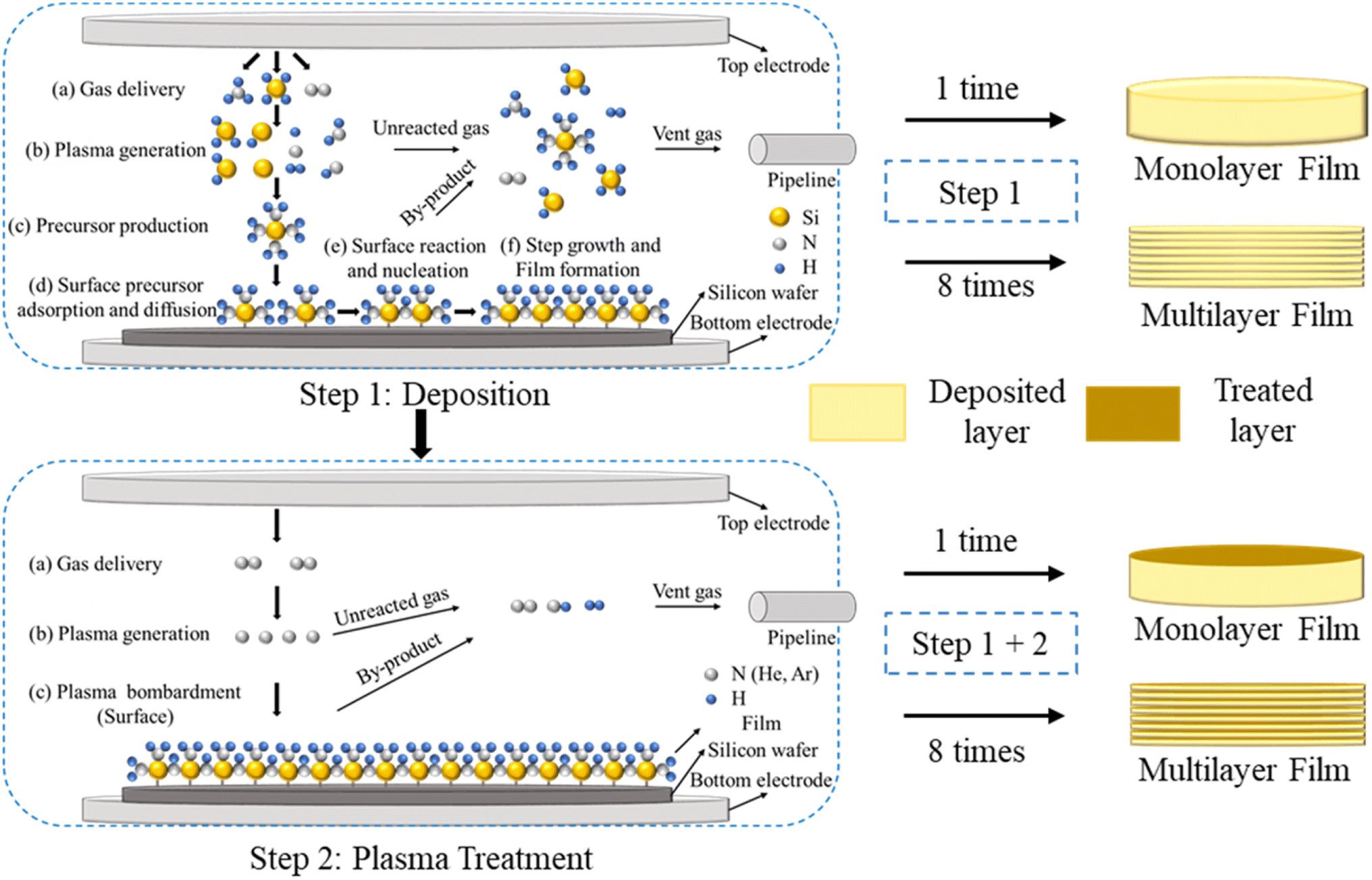
SiNx:H films were deposited on the surface of 12-inch p-type (100) silicon wafers using PECVD equipment provided by PF-300T (China). SiH4, NH3, N2, He, and Ar were utilized during the deposition and plasma treatment process, with each gas having a purity exceeding 99.99%. The deposition and treatment process of SiNx:H film is shown in Fig. 1. For monolayer SiNx:H films, step 1 involves depositing the silicon nitride film using SiH4, NH3, and N2 gases. Step 2 entails treating the film surface with He, Ar, or N2 plasma. For multilayer SiNx:H films, steps 1 and 2 are repeated until the desired thickness is achieved. The film prepared through n repetitions of steps 1 + 2 can be named He-n, Ar-n, and N2-n. In this manuscript, the monolayer and multilayer SiNx:H films (2, 4, 8, 12, 18, and 24 layers) were constructed and characterized. Meanwhile, the reference sample was constructed by repeating step 1 to investigate the stress influence mechanism of plasma bombardment on the SiNx:H film in greater depth. The film prepared through n repetitions of step 1 can be named Ref.-n. Based on our team's prior research experience, the fundamental deposition and treatment conditions are summarized in Table 1.
 |
| | Fig. 1 Schematic of the deposition and treatment process of the SiNx:H film.32 | |
Table 1 Deposition and treatment conditions of the SiNx:H film
| |
Temperature (°C) |
RF power (W) |
Electrode plate spacing (mm) |
Pressure (Torr) |
SiH4![[thin space (1/6-em)]](https://www.rsc.org/images/entities/char_2009.gif) :NH3:N2 gas flow ratio :NH3:N2 gas flow ratio |
He/Ar/N2 (sccm) |
Time (s) |
| Deposition |
400 |
130 |
15 |
5.4 |
1:10:40 |
— |
24 |
| Treatment |
400 |
300 |
15 |
5.4 |
|
5000 |
10 |
2.2 Characterization methods
2.2.1 Film stress. The internal stress (σf) of the SiNx:H film was calculated using the Stoney in eqn (1), which was determined using T910 (Skyverse Technology, China).| |
 | (1) |
where Es, ts, and Vs are Young's modulus, Poisson's ratio, and the thickness of the silicon wafer, respectively. Rs and Rf represent the curvature radii of the wafer before and after film deposition. Stress data were acquired from measurements carried out on five wafers.The Δσf of the film was used to indicate the difference in stress with or without plasma bombardment, which was calculated using eqn (2).
where Δ
σf−1 is the stress of the film constructed by repeating step 1; Δ
σf−1+2 is the stress of the film constructed by repeating steps 1 and 2.
2.2.2 Chemical bonds. Si–H, N–H and Si–N in SiNx:H films were analyzed using Fourier-transform infrared spectroscopy (FT-IR, Nicolet, USA). Spectral measurements were conducted over a wavenumber range of 4000 to 400 cm−1, with a resolution of 2 cm−1. Based on the obtained spectra, the density of Si–H and N–H bonds (ρSi–H, ρN–H) within the film was calculated using eqn (3). The proportion of hydrogen atoms in Si–H or N–H (HSi–H, HN–H) bonds relative to all atoms was computed using eqn (4). The overall atomic percentage of hydrogen present in Si–H and N–H bonds (Hsum) was evaluated using eqn (5). Furthermore, the ratio of bond densities between N–H and Si–H (RN–H/Si–H) was determined using eqn (6).30 The N/Si atomic ratio of films was tested by X-ray photoelectron spectroscopy (Nexsa G2, Thermo Fisher Scientific, USA). The etching process duration and the energy of the ion beam were set to 30 s and 50 eV, respectively.| |
 | (3) |
| |
 | (4) |
| |
 | (5) |
| |
 | (6) |
where SSi(N)–H is the absorption peak area of Si–H or N–H bonds in the film. φSi(N)–H is the cross-section of the Si–H or N–H bond, φSi–H and φN–H are 7.4 × 10⁻¹⁸ and 5.3 × 10⁻¹⁸ cm2, respectively, and THK is the thickness of the film.
2.2.3 Thickness. The thickness of the SiNx:H film was characterized using an 8500 spectrometer (KLA, USA) within a wavenumber range of 200 to 800 cm−1. Data were collected from five wafers, with 49 measurement points sampled on each wafer. Based on the thickness test results, the ΔTHK of film was used to indicate the difference in film thickness with or without plasma bombardment, which was calculated using eqn (7).where THK1 is the thickness of the film constructed by repeating step 1; THK1+2 is the thickness of the film constructed by repeating steps 1 and 2.
2.2.4 Refractive index. The refractive index of the SiNx:H film was characterized using an 8500 spectrometer (KLA, USA) within a wavenumber range of 200 to 800 cm−1. Data were collected from five distinct wafers, with 49 measurement points sampled on each wafer.
2.2.5 SEM image. Cross-sections of the samples were prepared using a FIB (Helios 5 HX, Thermo Fisher Scientific) with Ga+ ions and an acceleration voltage of 30 keV. A protective platinum layer was deposited on the top surface. Cross-sectional imaging of the film was performed using SEM.
3 Results and discussion
3.1 Film stress
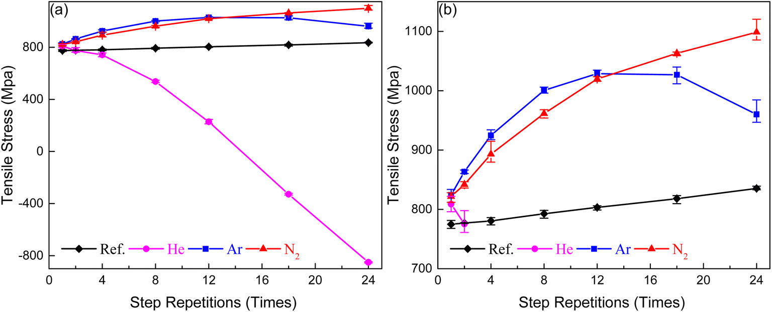
As shown in Fig. 2a, the stress of monolayer SiNx:H films can be enhanced by 4.39%, 6.37%, and 6.05% through He, Ar, and N2 plasma bombardment, respectively. However, the enhancement of film stress is constrained due to the limited bombardment depth. Therefore, the layered silicon nitride structure was constructed to further increase the tensile stress of the silicon nitride film. It can be seen from Fig. 2b that the stress of the multilayer SiNx:H film treated by N2 plasma increases as the number of repetitions increases. The stress of the 24-layer SiNx:H film treated with N2 plasma is 41.80% greater than the monolayer film. Similarly, the stress of the multi-layer SiNx:H film after Ar plasma treatment increases and then decreases with a greater number of layers. The stress of the 16-layer SiNx:H film treated with Ar plasma is also 32.78% greater than the monolayer film. However, as the number of layers increases, the stress of the He plasma-treated multilayer SiNx:H film decreases, with a maximum reduction of 1626 MPa, which indicates that not all plasma bombardments can improve the stress of multilayer SiNx:H film.
 |
| | Fig. 2 The effect of He, Ar, and N2 plasma bombardment on the stress of films (a) and an enlarged version of (a) and (b). | |
It also can be seen from Fig. 2a that the tensile stress of a multi-layer silicon nitride film can be significantly increased through repeated deposition processes in the absence of plasma bombardment. For silicon nitride films of similar thickness, an increase in the number of deposition cycles leads to a corresponding rise in stress, with the maximum stress increase of 7.80%. After eliminating the influence of repeated deposition on the increase of stress, the effects of N2 and Ar treatment on the enhancement of film stress are recalculated. Ar and N2 bombardment can enhance the stress of multi-layered silicon nitride films by up to 29.09% and 33.99%, respectively. The enhancement mechanisms of stress in multilayer silicon nitride films by Ar and N2 will be analyzed in Section 3.6.
3.2 Chemical bonds
The effect of He, Ar, and N2 plasma bombardment on the Si–H and N–H bonds of SiNx:H film was shown in Fig. 3. It can be seen from Fig. 3a that films subjected to He, Ar, or N2 plasma bombardment exhibit a markedly lower Hsum compared with SiNx:H films constructed by repeated deposition. For the 24-layer silicon nitride film, Hsum was reduced by 37.00%, 34.46%, and 40.82%, respectively following plasma bombardment using He, Ar, and N2. There was no significant difference in Hsum among the films subjected to three different types of plasma bombardment. However, there are notable differences in the RN–H/Si–H among the films prepared under the three different types of plasma treatments.
 |
| | Fig. 3 The effect of He, Ar, and N2 plasma bombardment on the (a) Hsum and (b) RN–H/Si–H of films. | |
It is obvious from Fig. 3b that RN–H/Si–H increased by 367.74%, 17.95%, and 78.33% following plasma bombardment using He, Ar, and N2, respectively for the 24-layer silicon nitride film. As shown in Fig. 4c, for N2-24, the increase in RN–H/Si–H is related to the reaction between N2 plasma and Si/N–H on the film surface. The N plasma not only promotes the cleavage of Si–H and N–H bonds but also reacts with Si–H to form Si–N–H bonds. However, the He and Ar plasmas can induce the cleavage of Si–H and N–H bonds but do not react with Si–H to form Si–N–H bonds (Fig. 4b and c). Therefore, the increase in RN–H/Si–H suggests that Si–H is more susceptible to breakage under plasma bombardment compared with N–H, which is related to the higher bond dissociation energy of N–H (N–H 390.8 vs. Si–H 318.0 kJ mol−1).33,34 The high energy of Ar plasma results in a relatively small difference in the number of bond breaks between Si–H and N–H under Ar plasma bombardment; therefore, there is no significant increase in RN–H/Si–H following Ar plasma bombardment. Compared with Ar plasma, He plasma exhibits lower energy.35 Consequently, the number of broken Si–H bonds under He plasma bombardment exceeds that of N–H bonds.
 |
| | Fig. 4 Schematic of the plasma bombardment process on the film surface: (a) He plasma; (b) Ar plasma; (c) N2 plasma. | |
The N/Si atomic ratios of the SiNx:H film were determined using XPS. It can be seen from Fig. 5 that there is no significant difference in the Si/N ratio among samples Ref.-1, He-1, Ar-1, and N2-1. Meanwhile, the N/Si atomic ratios of He-24 and N2-24 are slightly more than those of Ref.-24 and Ar-24. The N/Si atomic ratios of Ref.-24, He-24, Ar-24, and N2-24 are 1.211, 1.225, 1.211, and 1.230, respectively. By comparing samples Ref.-1 and Ref.-24, it can be concluded that repeated deposition does not increase the N/Si ratio. The increase in the N/Si ratio is related to plasma bombardment. For N2-24, the increase in the N/Si ratio can be attributed to the formation of chemical bonds between N and Si. However, an increase in the N/Si ratio has been observed for He-24 in the absence of additional N doping. This phenomenon can be attributed to the residual He on the film surface following He plasma treatment (Fig. 4a). Smaller-sized He atoms (atomic radius: He 31 pm < H 51 pm) are more likely to adsorb onto the surface of the film or penetrate its near-surface region.36,37 Residual He can promote nitrogen chemistry within the plasma by generating metastable reactive species. These metastable species facilitate enhanced nitrogen incorporation into the SiNx:H film, leading to an increase in nitrogen bonding.38
 |
| | Fig. 5 The effect of He, Ar, and N2 plasma bombardment on the N/Si atomic ratio of films. | |
3.3 Thickness
The effect of He, Ar, and N2 plasma bombardment on the THK and ΔTHK of films are shown in Fig. 6. ΔTHK is used to quantify the effect of He, Ar, and N2 plasma bombardment on the thickness of multilayer silicon nitride films, thereby excluding the influence of repeated deposition. For films treated by Ar or N2 plasma, the THK decreases and ΔTHK gradually increases as step repetitions increase. The reason is that plasma bombardment can induce the rupture of Si–H and N–H bonds accompanied by the reconstruction of Si–N bonds, with the treated layer becoming more compact. The influence of He plasma bombardment on the film thickness differs from that of Ar or N2, which is like the stress effects observed for the three plasmas. For films treated by He plasma, the THK initially decreases and subsequently increases with a greater number of step repetitions. This phenomenon is related to the residual He in the film. At the initial stage of deposition, the residual He can increase N content within the film by generating metastable reactive species. This reduces the crosslinking density of the Si–N network, leading to volumetric expansion.
 |
| | Fig. 6 The effect of He, Ar, and N2 plasma bombardment on the (a) THK and (b) ΔTHK of films. | |
3.4 Refractive index
The effect of He, Ar, and N2 plasma bombardment on the refractive index of films is shown in Fig. 7a. As the number of repetitions increases, the refractive index gradually increases. Meanwhile, films subjected to He, Ar, or N2 plasma bombardment exhibit a markedly higher refractive index compared with SiNx:H films constructed by repeated deposition. Compared with Ref.-1, the refractive index of the SiNx:H film prepared by repeating the deposition process 24 times increased by 0.31%. For the 24-layer SiNx:H film, the refractive index decreased by 1.67%, 1.73%, and 1.82% following plasma bombardment using He, Ar, and N2, respectively. Under normal circumstances, the refractive index is primarily influenced by the N/Si ratio.39,40 However, given that the deposition process remains consistent and the variation in Si/N ratios is minimal in this study, the observed change in refractive index is not attributed to alterations in the N/Si ratio caused by plasma bombardment.
 |
| | Fig. 7 (a) The effect of He, Ar, and N2 plasma bombardment on the refractive index of films, and (b) the relationship between Hsum and the refractive index. | |
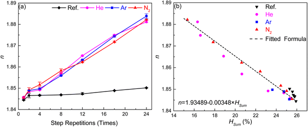
From the comparison between Fig. 3 and 7a, it is evident that the relationship between refractive index and Hsum has consistently demonstrated a stable correlation. To further elucidate the relationship between refractive index and Hsum, scatter plots of refractive index versus Hsum are presented in Fig. 7b. A linear regression model was employed to quantitatively characterize this relationship. The correlation coefficient (R2) of the fitted formula is 0.94409, indicating a strong positive correlation between refractive index and Hsum. This suggests that variations in refractive index are primarily attributed to changes in Hsum. The reason is that the Si–H and N–H bonds cleave under plasma bombardment, leading to the formation of Si–Si and Si–N bonds. As the atomic arrangement becomes more compact, the film density increases, leading to an increase in the refractive index. This result aligns with previous studies, where the Lorentz–Lorenz formula shows that the refractive index of film exhibits a pronounced linear relationship with density.41,42 The refractive index exhibits a linear correlation with density and Hsum, indirectly corroborating that a reduction in Hsum leads to an increase in film density.
3.5 SEM cross-sectional images
The SiNx:H film treated by He, Ar, and N2 plasma and reference sample are shown in Fig. 8. It can be seen from Fig. 8a that films prepared through a three-step deposition process exhibit no significant evidence of delamination without plasma bombardment. Meanwhile, the phenomenon of stratification is not visible with plasma bombardment (Fig. 8b–d). This might be related to the SEM resolution, and it also indicates that the thickness of the treated layer is markedly lower than that of the deposited layer.
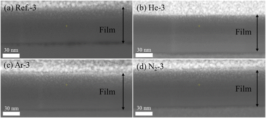 |
| | Fig. 8 Cross-sectional imaging of morphology: (a) Ref.-3; (b) He-3; (c) Ar-3; (d) N2-3. | |
3.6 Discussion
The stress of the SiNx:H film can be primarily categorized into two types: intrinsic stress and thermal stress. The intrinsic stress can be attributed to factors such as lattice mismatch, crystal defects, and differences in unit cell parameters, among others.43 Thermal stress is related to the coefficient of thermal expansion of the film.44 In this study, the film was deposited under identical parameters, and the thickness of the treated layer is nearly imperceptible and markedly lower than that of the deposited layer as evidenced by the SEM images (Fig. 7), thus only exerting a minimal impact on the coefficient of thermal expansion. Meanwhile, during the entire deposition and plasma bombardment processes, the temperature exhibited controlled fluctuations within a range of 400 ± 10 °C. Consequently, the possibility of stress enhancement caused by significant temperature fluctuations was effectively excluded. Therefore, it can be inferred that the change in the stress of the film following plasma bombardment can be primarily attributed to variations in intrinsic stress, rather than the effects of thermal stress.
Following bombardment by N2 or Ar plasma, both monolayer and multilayer films exhibited significant and varying degrees of tensile stress enhancement. The reason is that plasma bombardment can induce the rupture of Si–H and N–H bonds accompanied by the reconstruction of Si–N bonds, leading to densification through chemical bond reorganization in the treated surface layer (Fig. 9a square frame). This structural evolution propagates stress coupling effects to non-treated regions, inducing anisotropic displacement of the lattice along normal and in-plane directions (Fig. 9a circular frame), thereby triggering a significant enhancement in the tensile stress of the film. Based on the above stress evolution mechanism, this study successfully established a quantitative model between the ΔTHK and Δσf. As illustrated in Fig. 10, this model follows an exponential relationship, with a determination coefficient R2 = 0.94017, indicating a high degree of fitting accuracy. Meanwhile, it also can be seen that the Si–N peaks of Ar-1/24 and N2-1/24 shift to a lower wavenumber compared with the Si–N peaks of Ref.-1/24 (Fig. 11), suggesting a decrease in the bond force constant of Si–N, which is consistent with the elongation of chemical bonds within the marked circular region in Fig. 9a.45 This experimental evidence further substantiates that the observed increase in tensile stress is primarily attributed to the enhancement of the film's intrinsic stress induced by plasma bombardment.
 |
| | Fig. 9 Schematic of (a) surface structural changes in the film following plasma bombardment; (b) silicon nitride structure deposited without He; (c) silicon nitride structure deposited with He. | |
 |
| | Fig. 10 Relationship between the ΔTHK and Δσf of films treated with N2 and Ar plasma. | |
 |
| | Fig. 11 FT-IR spectrum of (a) monolayer silicon nitride films and (b) multilayer silicon nitride films. | |
The tensile stress in monolayer films can be enhanced by He plasma bombardment. For monolayer film, the stress induction mechanism through He plasma bombardment exhibits consistency with those observed under Ar or N2 plasma bombardment. If only the surface bombardment process is considered, He plasma bombardment should also exhibit an enhancing effect on the stress of multilayer films. However, unlike multilayer films treated with Ar or N2 plasma, the stress in multilayer films treated with He plasma exhibits a decreasing trend as the number of layers increases. When the number of layers exceeds 18, the films transition from tensile to compressive stress. The reduction in tensile stress is attributed to the residual He within the film. During the initial phase of each deposition process, the residual He can promote nitrogen chemistry within the plasma and enhance nitrogen incorporation into the a-SiN:H film. The increase in N content within the film reduces the cross-linking degree of the Si–N network structure (Fig. 9b and c square frame), inducing volumetric expansion. This expansion compresses the underlying Si–N network (Fig. 9b and c circular frame), leading to a progressive decrease in tensile stress and ultimately resulting in a transition to compressive stress.46 This phenomenon has also been confirmed in the FT-IR spectra. It can be seen that the Si–N peaks of He-24 shift to a higher wavenumber compared with Ref.-24 (Fig. 11b), suggesting an increase in the bond force constant of Si–N, which is consistent with the shortening of the chemical bond length within the marked circular region in Fig. 9b and c.
4 Conclusion
In this study, the multilayer silicon nitride films are constructed by repeating deposition and plasma treatments. Based on the test results of stress, chemical bonds, THK, refractive index, and the transverse section image, the influence mechanism of He, Ar, and N2 plasma bombardment on the monolayer and multilayer silicon nitride films of stress is investigated and compared in greater depth. The conclusions are summarized as follows:
(1) Following bombardment by N2 or Ar plasma, both monolayer and multilayer films demonstrated significant yet distinct enhancements in tensile stress. Multilayer SiNx:H films treated with N2 and Ar plasma exhibited 41.80% and 32.78% higher stress, respectively compared with their monolayer films. He plasma bombardment also enhanced the tensile stress in monolayer films. However, He plasma treatment induced a progressive stress inversion in multilayered films, evolving from tensile-dominated to compressive-oriented states.
(2) Exposure to N2 or Ar plasma induces bond cleavage of Si–H, and N–H species, followed by reorganization of Si–N networks, which triggers structural compaction through chemical rearrangement in treated layers. These morphological changes propagate stress coupling phenomena to neighboring untreated zones, generating directional lattice distortions along perpendicular and planar axes, consequently elevating the film's tensile stress magnitude.
(3) Multilayer films treated by He plasma exhibit a gradual transition from tensile to compressive stress, which can be attributed to residual He during the plasma treatment process. At the initial stage of deposition, the residual He can increase nitrogen content within the film by generating metastable reactive species. This reduces the cross-linking density of the Si–N network, leading to volumetric expansion and subsequent compression of the underlying structure.
Data availability
The data supporting this article have been included as part of the manuscript. For requests about the original data, please do not hesitate to contact the corresponding author.
Author contributions
Jianping Ning: conceptualization, writing – original draft, writing – review & editing, data curation, and resources; Zhen Tang: writing – original draft, data curation; data curation, and Yue Sun: methodology and visualization; Chunjie Niu: investigation; Jichi Yang: methodology and data curation; Dayu Zhou: writing – review & editing and project administration.
Conflicts of interest
There is no conflict of interest in this article.
Acknowledgements
This project was supported by Piotech Technology Co., Ltd. and includes film deposition and film property measurements.
References
- G. La Penna, C. Mancini, A. Proietti, L. Buccini, D. Passeri, N. Gambacorti, J. Richy and M. Rossi, Appl. Spectrosc., 2024, 78, 1245–1255 CrossRef CAS PubMed.
- H. Q. Xu, J. X. Yao, Z. Z. Yang, L. Cao, Q. Z. Zhang, Y. L. Li, A. Y. Du, H. X. Yin and Z. H. Wu, IEEE Trans. Electron. Dev., 2023, 70, 3365–3371 Search PubMed.
- W.-S. Liao, Y.-G. Liaw, M.-C. Tang, K.-M. Chen, S.-Y. Huang, C. Y. Peng and C. W. Liu, IEEE Electron Device Lett., 2008, 29, 86–88 CAS.
- P. Yang, W. S. Lau, S. W. Lai, V. L. Lo, L. F. Toh, J. Wang, S. Y. Siah and L. Chan, J. Appl. Phys., 2010, 108, 034506 CrossRef.
- C. Schade, A. Phan, K. Joslin and F. E. Talke, Microsyst. Technol., 2021, 27, 2263–2268 CrossRef CAS.
- K. Bae, M. Jin, H. Lim, L. Hwang, D. Shin, J. Park, J. Heo, J. Lee, J. Do, I. Bae, C. Jeon and J. Park, Behaviors and Physical Degradation of HfSiON MOSFET Linked to Strained CESL Performance Booster, 2011 International Reliability Physics Symposium, IEEE, Monterey, CA, 2011 Search PubMed.
- G. Beylier, S. Bruere, D. Benoit and G. Ghibaudo, Microelectron. Reliab., 2008, 48, 1539–1543 CrossRef.
- L.-Q. Yang, C. Zhang, W.-L. Li, G.-H. Liu, M. Wu, J.-Q. Liu and J.-H. Zhang, Adv. Manuf., 2023, 11, 181–190 Search PubMed.
- B. Shu, H. Zhang, R. Xuan, X. Dai, H. Hu, J. Song, L. Liang and J. Cui, Fabrication of high compressive stress silicon nitride membrane in strained silicon technology, 2009 IEEE International Conference of Electron Devices and Solid-State Circuits (EDSSC), IEEE, Xian, People's Republic of China, 2009 Search PubMed.
- R. Arghavani, L. Xia, H. M'Saad, M. Balseanu, G. Karunasiri, A. Mascarenhas and S. E. Thompson, IEEE Electron Device Lett., 2006, 27, 114–116 Search PubMed.
- K. N. Subhani, N. Remesh, S. Niranjan, S. Raghavan, R. Muralidharan, D. N. Nath and K. N. Bhat, Solid-State Electron., 2021, 186, 108188 Search PubMed.
- S. Deleonibus, Eur. Phys. J.: Appl. Phys., 2006, 36, 197–214 Search PubMed.
- M. P. Hughey and R. F. Cook, Thin Solid Films, 2004, 460, 7–16 Search PubMed.
- Q. Xu, W. Xiong, G. Wang and T. Ye, J. Mater. Sci. Mater. Electron., 2020, 31, 10078–10083 CrossRef CAS.
- P. Morin, D. Benoit and J. Metz, Eur. Phys. J.: Appl. Phys., 2008, 43, 315–320 Search PubMed.
- M. P. Hughey and R. F. Cook, MRS Online Proc. Libr., 2003, 795, 235–240 Search PubMed.
- M. Belyansky, M. Chace, O. Gluschenkov, J. Kempisty, N. Klymko, A. Madan, A. Mallikarjunan, S. Molis, P. Ronsheim, Y. Wang, D. Yang and Y. Li, J. Vac. Sci. Technol., A, 2008, 26, 517–521 CrossRef CAS.
- P. Morin, E. Martinez, F. Wacquant and J. L. Regolini, MRS Online Proc. Libr., 2005, 875, 146 CrossRef.
- J. Tian, B. Zuo, W. Lu, M. Zhou and L. C. Hsia, Jpn. J. Appl. Phys., 2010, 49, 05fb01 CrossRef.
- H. H. Radamson, X. He, Q. Zhang, J. Liu, H. Cui, J. Xiang, Z. Kong, W. Xiong, J. Li, J. Gao, H. Yang, S. Gu, X. Zhao, Y. Du, J. Yu and G. Wang, Micromachines, 2019, 10, 293 CrossRef PubMed.
- Y. Miyagawa, T. Murata, Y. Nishida, T. Nakai, A. Uedono, N. Hattori, M. Matsuura, K. Asai and M. Yoneda, Jpn. J. Appl. Phys., 2007, 46, 1984–1988 CrossRef CAS.
- V. Zubkov, M. Balseanu, L.-Q. Xia and H. M’Saad, MRS Online Proc. Libr., 2005, 910, 1904 Search PubMed.
- M. Belyansky, N. Klymko, A. Madan, A. Mallikarjunan, Y. Li, A. Chakravarti, S. Deshpande, A. Domenicucci, S. Bedell, E. Adams, J. Coffin, L. Tai, S. P. Sun, J. Widodo and C. W. Lai, MRS Online Proc. Libr., 2004, 863, B7.9 Search PubMed.
- P. Morin, G. Raymond, D. Benoit, D. Guiheux, R. Pantel, F. Volpi and M. Braccini, J. Vac. Sci. Technol., A, 2011, 29, 041513 CrossRef.
- A. V. Novak, V. R. Novak, A. A. Dedkova and E. E. Gusev, Semiconductors, 2018, 52, 1953–1957 CrossRef CAS.
- M. A. Lieberman and A. J. Lichtenberg, Principles of Plasma Discharges & Materials Processing, 2008, vol. 11, p. 800 Search PubMed.
- W. Shang, D. Wang and Y. Zhang, Phys. Plasmas, 2008, 15, 093503 Search PubMed.
- M. Laroussi, IEEE Trans. Plasma Sci., 2015, 43, 703–712 CAS.
- S. National Institute of and Technology, NIST Chemistry WebBook: Argon, 2023, https://webbook.nist.gov/cgi/cbook.cgi?ID=C7440371 Search PubMed.
- K. Kamataki, Y. Sasaki, I. Nagao, D. Yamashita, T. Okumura, N. Yamashita, N. Itagaki, K. Koga and M. Shiratani, Mater. Sci. Semicond. Process., 2023, 164, 107613 Search PubMed.
- L. Zheng, L. Deng, J. Liu, Y. Ma and Y. Cheng, SMT Optimization of PMOSFET Based on Multi-Deposition and In-Situ N2 Plasma Treatment, 2024 Conference of Science and Technology for Integrated Circuits (CSTIC), Shanghai, People's Republic of China, 2024 Search PubMed.
- J. Ning, Z. Tang, L. Chen, B. Li, Q. Wu, Y. Sun and D. Zhou, Electronics, 2024, 13, 2779 CrossRef CAS.
- X. Xu, Q. He, T. Fan, Y. Jiang, L. Huang, T. Ao and C. Ma, Appl. Surf. Sci., 2013, 264, 823–831 Search PubMed.
- L. Zhao, W. Zhang, J. Chen, H. Diao, Q. Wang and W. Wang, Front. Energy, 2017, 11, 85–91 Search PubMed.
- Y. V. Bludov, D. A. Bahamon, N. M. R. Peres and C. J. S. De Matos, J. Opt. Soc. Am. B, 2024, 41, 626–636 CrossRef CAS.
- J. K. Yao, S. Chen, X. W. Sun and H. S. Kwok, Appl. Surf. Sci., 2015, 355, 702–705 Search PubMed.
- V. Martirosyan, E. Despiau-Pujo, J. Dubois, G. Cunge and O. Joubert, J. Vac. Sci. Technol., A, 2018, 36, 041301 CrossRef.
- M. J. Loboda and J. A. Seifferly, J. Mater. Res., 1996, 11, 391–398 CrossRef CAS.
- D. Benoit, P. Morin and J. Regolini, Thin Solid Films, 2011, 519, 6550–6553 Search PubMed.
- H. Mäckel and R. Lüdemann, J. Appl. Phys., 2002, 92, 2602–2609 CrossRef.
- J. Ji, Y. Yan, Y. Chen, E. Ha, C. Hao and P. Lei, China Plast., 2024, 38, 7–12 Search PubMed.
- E. E. Khawaja, F. Bouamrane, F. Aladel, A. B. Hallak, M. A. Daous and M. A. Salim, Thin Solid Films, 1994, 240, 121–130 CrossRef CAS.
- C.-C. Lee, Y.-Y. Liou, C.-P. Chang, P.-C. Huang, C.-Y. Huang, K.-C. Chen and Y.-J. Lin, Surf. Coat. Technol., 2022, 434, 128225 Search PubMed.
- J. G. Kim and J. Yu, Mater. Sci. Eng. B, 1998, 57, 24–27 CrossRef.
- I. Guler, Mater. Sci. Eng. B, 2019, 246, 21–26 CrossRef CAS.
- C. Iliescu, M. Avram, B. Chen, A. Popescu, V. Dumitrescu, D. P. Poenar, A. Sterian, D. Vrtacnik, S. Amon and P. Sterian, J. Optoelectron. Adv. Mater., 2011, 13, 387–394 Search PubMed.
|
| This journal is © The Royal Society of Chemistry 2025 |
Click here to see how this site uses Cookies. View our privacy policy here. 
 Open Access Article
 This Open Access Article is licensed under a Creative Commons Attribution-Non Commercial 3.0 Unported Licence
 *a
*a