
 Open Access Article
 This Open Access Article is licensed under a Creative Commons Attribution-Non Commercial 3.0 Unported Licence
Fabrication of a self-powered broadband photodetector by 50% replacement of Pb by Mg in the CH3NH3Pb0.5Mg0.5Cl2I perovskite lattice†
Kumaar Swamy Reddy
B.
ab,
Smrutiranjan
Panda
a,
Easwaramoorthi
Ramasamy
 a,
Sushmee
Badhulika‡
*b,
Ganapathy
Veerappan§
*a and
Pramod H.
Borse
*a
a,
Sushmee
Badhulika‡
*b,
Ganapathy
Veerappan§
*a and
Pramod H.
Borse
*a
aCentre for Solar Energy Materials, International Advanced Research Centre for Powder Metallurgy and New Materials, Balapur PO, Hyderabad, Telangana 500 005, India. E-mail: phborse@arci.res.in; ganagv@arci.res.in; Fax: +91 40 2444 2699; Tel: +91 40 2445 2426
bDepartment of Electrical Engineering, Indian Institute of Technology – Hyderabad, Kandi, Sangareddy, Hyderabad, India
First published on 29th August 2023
Abstract
Methyl ammonium lead halide (MAPbX3) suffers from high toxicity of the Pb2+ cation leading to a major roadblock to its end-application. To alleviate the toxicity issue, a complete or partial substitution of Pb2+ by eco-friendly Mg-ions is attempted in the present study. The substitution of Pb2+ with Mg2+ cations in the MAPbX3 crystal structure was carried out by tuning the stoichiometry of Mg2+ in MAPbxMg1−xCl2I (for x = 0.1, 0.3, 0.5, 0.7, 0.9). Here MAPbxMg1−xCl2I has been demonstrated for the first time in the application of a self-powered photodetector. A facile one-step anti-solvent approach has been used to synthesize the hybrid halide perovskite. Systematic structural and optical characterization indicates the formation of the desired tetragonal perovskite phase that exhibits a bandgap of 1.5–1.6 eV. The synthesized MAPbxMg1−xCl2I has been used for device fabrication with (i) a simple hole transport material (HTM)-free configuration, and (ii) an economical carbon as the top electrode contact. MAPb0.5Mg0.5Cl2I perovskite was found to be the best performing device, with an excellent responsivity of 153.74 mA W−1 at zero bias, high detectivity of 6.5 × 10¹⁰ Jones, and a fast response/recovery time of 411 ms/50 ms. The optimum Mg substituted perovskite film thus yields an eco-friendly option compared to the conventional MAPbX3 with nearly 50% replacement of the toxic Pb by benign Mg2+ cations. The demonstration of a MAPb0.5Mg0.5X3-based novel performance photodetector thus paves an important path to the replacement of toxic Pb2+ in perovskite opto-electronic devices, thereby leading to eco-friendly devices.
1. Introduction
Recently, hybrid perovskites have been at the core of opto-electronic research, due to their applications in solar cells, LEDs, photodetectors, etc.1,2 Among them, methyl ammonium lead iodide (MAPbI3) has become a conventional photoabsorber due to its excellent opto-electronic properties, such as high optical absorption coefficient (105 cm−1), bandgap tunability (1.5–2.9 eV), large diffusion length (1 μm), ambivalent carrier transport, high carrier mobility (10 cm2 V−1 s−1), low-excitonic energy (10 meV) and direct band gap (1.51 eV).3–8 Despite its excellent photo-absorption capability, it is still far from commercialization due to two major issues: (1) the presence of toxic heavy Pb2+ metal cation, and (2) its inherent instability towards heat, moisture and intense light beams, which limits its operating conditions.9 Accordingly, it has become very important to develop new perovskite systems, that completely or partially substitute the toxic lead (Pb2+) cation with eco-friendly abundant metal cations. We attempt here to utilize magnesium, an alkaline earth metal ion to replace the toxic lead metal-ion.It is known that a hybrid perovskite with ABX3 structure contains A+, the larger cation, which can be either organic (methyl ammonium, formamidium), inorganic (Cs, Ag) or a mixture of both, at the B2+ site, the smaller metal cation (Pb2+), and X3− as the halide anion. In order to substitute the Pb2+ with any other metal cation, one of the following rules must be satisfied: (a) the replacing metal-ion has the same valency as Pb2+; (b) one monovalent metal ion and one tri-valent ion can be used to replace Pb2+; OR (c) one tetra-valent metal ion and one vacancy site can be accommodated for Pb2+ substitution.10 In the past, various metal cations have been explored for such apurpose by using Sn2+, Ge2+, Cu2+ (bi-valent); Bi3+, Sb3+, In3+ (tri-valent), Cu+ or Ag+ (mono-valent).11 Mainly, Sn2+ has been extensively potentially used for lead substitution.12 In 2014, Ogomi et al. reported the synthesis of Sn/Pb mixed halide and its application as a solar cell absorber film.13 The system with Sn, i.e. MASnI3, exhibited a decreased bandgap in comparison with MAPbI3. Since then, extensive research has been done on Sn-based perovskites for various applications, like LEDs and photodetectors. Nonetheless, though they exhibited good performance, their end-use for practical applications has been severely hampered by their toxicity and high intrinsic defect states. Specifically, the Sn2+ ion tends to oxidise very fast to Sn4+, thereby yielding a distortion in the perovskite structure.14 Therefore, it is crucial to identify an eco-friendly metal for the replacement of the toxic Pb2+. In this context, alkaline earth cations such as Ca2+, Ba2+, Mg2+, Sr2+, and Be2+ display high potential, due to their inherent benignity and high earth-abundance.15 In the past, a theoretical study estimated the bandgaps of the ACaX3, ASrX3 and ABaX3 families and they were found to lie beyond 3.0 eV, thus making them unsuitable for photovoltaics and broadband photodetectors.16 However, the theoretical studies on Mg-based perovskites predicted them to exhibit a narrow bandgap of 1.3–1.8 eV, thus making them suited for photovoltaic applications.17 In another report, the effect of Mg substitution at the Pb site on the absorption coefficient and solar cell efficiency was reported via first-principles calculations.18 It was observed that, with the doping of Mg in the MAPbI3 lattice, the bandgap decreased slightly close to the optimal solar bandgap; however, the absorption coefficient is also reduced marginally. In 2018, Hayase et al. reported the impact of doping of MgCl2 in MAPbI3 for solar cells. It was seen that, with 1% doping of Mg, it showed improvement in the device efficiency and stability.19 In another work, the synthesis of MAPbxMg1−xX3 perovskite was first reported, where it was synthesized by the solid state reaction technique, with the Mg concentration varied from 0.1 to 0.9%, but it was in a photo-absorber application in a solar cell.20 Despite Mg being predicted to be a potential candidate for toxic Pb2+ substitution, there are no reports on the utilization of Mg-doped perovskites for photodetector applications. Thus we selected this system for photodetector application.
The salient feature of this work is the fabrication of a photodetector with a hole transport layer (HTL) free configuration and the utilization of economic conducting carbon as the top electrode contact material. In most of the perovskite self-powered photodetectors, separate (i) electron transport layers (ETLs) and (ii) hole transport layers (HTLs) are employed for an efficient charge extraction. The usage of traditional HTLs such as spiro-OmeTAD or PEDOT:PSS results in faster degradation of devices due to their reaction with the underneath perovskite films, thus making it non-cost-effective.21,22 Hence, it is highly desirable to get rid of such HTL organic transport layers.
In this work, novel MAPbxMg1−xX3 (x = 0.1, 0.3, 0.5, 0.7, 0.9) perovskite was synthesized and utilized to demonstrate the fabrication of a self-powered photodetector. It was synthesized using a facile one-step anti-solvent approach, and the film was deposited on a mesoporous-TiO2 layer. Thus, the fabricated photodetector was found to operate as a self-powered device due to the built-in potential induced at the TiO2/perovskite junction, which displayed a wide response in the UV to visible range.
2. Experimental
2.1 Materials
Titanium diisopropoxide bis(acetylacetonate), hydroiodic acid (HI), hydrochloric acid (HCl), diethyl ether (DEE), toluene, lead chloride (PbCl2), magnesium chloride (MgCl2), 2-propanol (98%), dimethyl sulfoxide (DMSO) and 1-butanol were purchased from Sigma Aldrich. Methylamine was purchased from TCI Chemicals, India Pvt. Ltd. TiO2 sol is procured from Dyesol.2.2 Instrumentation
Structural analysis of the films was performed by X-ray diffraction studies using a Rigaku XRD diffractometer with a Cu Kα X-ray source. A UV-Vis-NIR spectrophotometer (Model Cary 5000) working in the range of 300–1000 nm was employed for the optical absorption studies. A Field-Emission Scanning Electron Microscope (MODEL Gemini 500) has been used for film morphology imaging. Opto-electronic studies were performed using a Princeton Applied Research electrochemical workstation with a Model VERSASTAT 4 Potentiostat/galvanostat. A Newport Cornerstone™ 260 1/4m Monochromator is used for spectral responsivity testing.2.3 Cleaning and patterning of FTO and TiO2 deposition
Substrate preparation and ETL fabrication (both c-TiO2 and m-TiO2) were done as per our previously reported articles. FTO glasses were etched using 4 mM hydrochloric acid (HCl) and zinc powder. The etched FTOs were cleaned with DI water and organic solvents. The dried substrates were cleaned once more for 15 minutes with UV-Ozone. A 70 nm thin c-TiO2 layer was deposited by spin-coating titanium diisopropoxide bisacetylacetonate solution (0.15 M and 0.3 M) in butanol. After coating, the substrates were heated at 500 °C for 30 minutes. Next, a 350 nm m-TiO2 layer was deposited by spin coating m-TiO2 sol and heated at 500 °C for 30 minutes. The substrates were ready for perovskite deposition after ETL fabrication.2.4 Perovskite deposition and device fabrication
Synthesis of methyl ammonium iodide was carried out as per earlier reports from our lab.23,24 To optimize the Mg/Pb ratio, five distinct perovskite precursor solutions were made by varying the ratios of magnesium chloride (MgCl2) and lead chloride (PbCl2). MAMgxPb1−xCl2I perovskite precursor solutions were prepared by mixing 1 M methyl ammonium iodide (MAI) with MgCl2 and PbCl2 in molar ratios of 0.1 M![[thin space (1/6-em)]](https://www.rsc.org/images/entities/char_2009.gif) :0.9 M, 0.3 M:0.7 M, 0.5 M:0.5 M, 0.7 M:0.3 M, and 0.9 M:0.1 M in DMSO and stirred for two hours at room temperature. The perovskite layer was deposited on ETL-coated FTO substrates by spin-coating the precursor solution at an acceleration rate of 4000 rpm for 25 s. The anti-solvent toluene was slowly dropped at 10 s before the spin coating ended and annealed at 75 °C for 10 minutes. As the cathode, a carbon layer was created by doctor blading carbon paste and annealed at 75 °C for 5 minutes.
:0.9 M, 0.3 M:0.7 M, 0.5 M:0.5 M, 0.7 M:0.3 M, and 0.9 M:0.1 M in DMSO and stirred for two hours at room temperature. The perovskite layer was deposited on ETL-coated FTO substrates by spin-coating the precursor solution at an acceleration rate of 4000 rpm for 25 s. The anti-solvent toluene was slowly dropped at 10 s before the spin coating ended and annealed at 75 °C for 10 minutes. As the cathode, a carbon layer was created by doctor blading carbon paste and annealed at 75 °C for 5 minutes.
Then all the perovskite precursor solutions were filtered using a PTFE chromatography filter and spin coated on top of m-TiO2 coated substrates, with antisolvent toluene added at the last 10 s of spin coating. Then, the films were annealed at 75 °C for 5 minutes to form the perovskite crystal. The carbon cathode was fabricated by doctor blading carbon paste on top of the perovskite layer. Fig. 1 schematically illustrates the perovskite preparation and device fabrication methodology. Table 1 lists the naming convention and precursor concentration used for fabrication of devices with varied Mg:Pb ratio.
 | ||
| Fig. 1 Pictorial illustration of (a) the preparation of the perovskite precursor and (b) the device fabrication process. | ||
:Pb ratio of the precursors used in the preparation of MAPb1−xMgxCl2I
| Sample name | Mg:Pb stoichiometric ratio |
Chemical formula | Composition of the precursors | ||
|---|---|---|---|---|---|
| MgCl2 | PbCl2 | MAI | |||
| Mg:Pb – 1:9 |
1:9 |
MAPb0.1Mg0.9X3 | 0.1 M | 0.9 M | 1 M |
| Mg:Pb – 3:7 |
3:7 |
MAPb0.3Mg0.7X3 | 0.3 M | 0.7 M | 1 M |
| Mg:Pb – 5:5 |
5:5 |
MAPb0.5Mg0.5X3 | 0.5 M | 0.5 M | 1 M |
| Mg:Pb – 7:3 |
7:3 |
MAPb0.7Mg0.3X3 | 0.7 M | 0.3 M | 1 M |
| Mg:Pb – 9:1 |
9:1 |
MAPb0.9Mg0.1X3 | 0.9 M | 0.1 M | 1 M |
3. Results & discussion
3.1 Structural and morphological studies
The XRD spectra of films deposited with various stoichiometric ratios of Mg:Pb are shown in Fig. 2. The synthesized films exhibit diffraction peaks at 14.18°, 25.04°, 28.26°, 28.52°, 31.52° and 33.62° corresponding to the (110), (202), (004), (220), (114) and (204) planes, respectively. The obtained diffraction peaks are ascribed to the characteristic peaks of the tetragonal perovskite crystal system (space group: I4/mcm).25,26 This confirms that all the films prepared with the varied ratios of Mg:Pb crystallize in the perovskite structure. This also ascertains that incorporation of the Mg2+ cation in the pristine MAPbX3 perovskite does not significantly alter or distort the inherent perovskite structure, despite the significant difference in the ionic radii of Pb2+ and Mg2+. It can be noted that the ionic radii of Pb2+ and Mg2+ are 118 pm and 76 pm, respectively. A similar phenomenon has been observed in literature reports where the large Pb2+ cation (118 pm) was partially replaced with comparatively smaller cations such as Fe2+ (92 pm), Ca2+ (100 pm), In3+ (80 pm), Mn2+ (70 pm) and Cd2+ (100 pm).10,20,27,28 Apart from the peaks corresponding to the perovskite crystal structure, peaks corresponding to other species and constituents such as MgCl2, PbI2 and TiO2 were also observed. It should be noted that with the increase in the inclusion of Mg, the relative intensity of the perovskite characteristic peak at 14.12° significantly enhanced. This indicates that the inclusion of Mg2+ significantly influences the preferred orientation of the crystallites towards the (110) plane. Apart from the relative intensity of the characteristic peak, its FWHM is also reduced, thus indicating the enhancement in the crystallinity of the films. The occurrence of the PbI2 peak in the perovskite is owing to the precursors MAI and PbCl2, which are used as the source for the iodide and chloride anions, respectively; those react to produce PbI2 as the by-product. Some reports on mixed halide perovskites do mention that the occurrence of PbI2 is due to the decomposition of the perovskite over time.29 Factually, it is well-known that the presence of a small amount of PbI2 is beneficial to the device performance. PbI2 passivates the perovskite grains, thus reducing the recombination rate and improving the carrier diffusion length. Some impurity peaks due to MAI, MgCl2 and PbCl2 were seen due to the unreacted precursors in the films. It can also be noted that the TiO2 layer that exists underneath the perovskite does expectedly contribute to the XRD spectra. Furthermore, the films Mg:Pb-5:5 and Mg:Pb-3:7 exhibit more peaks due to unreacted precursors and accordingly, the perovskite related peaks seem to be diminished, indicating the poor crystallization of the perovskite. In contrast, the Mg:Pb-5:5 and Mg:Pb 7:3 films exhibit significantly stronger diffraction peaks from the perovskite and the peak intensity from unreacted precursors and by-products drastically reduces. This denotes that the Mg:Pb-5:5 and Mg:Pb 7:3 films exhibit higher crystallization of the perovskite phase.
 | ||
| Fig. 2 XRD spectra of perovskite films with varied Mg:Pb ratios of (a) 1:9, (b) 3:7, (c) 5:5 and (d) 7:3, as we see top to bottom. | ||
The observation of TiO2 diffraction peaks in the X-ray diffraction spectrum of MAPb0.5Mg0.5X3 perovskite indicates the possible penetration of X-rays beyond the perovskite and interaction with the underlying TiO2 layer. The mesoporous nature of TiO2 results in infiltration of the perovskite film inside the pores of TiO2. Thus, when the X-rays are irradiated over the device, it is expected that the X-rays interact with both the perovskite and TiO2. The magnitude of penetration of X-rays in any material is influenced by the absorption coefficient and penetration depth. In MAPbI3, X-rays have an absorption coefficient of ∼0.5 μm−1, which corresponds to a penetration depth of 2 μm.30 Since the perovskite layer thickness is only in the range of a few hundreds of nanometers, it is obvious that the X-rays will penetrate and interact with the underlying TiO2 layer.
FE-SEM has been performed to study the surface morphology of the deposited thin films, as shown in Fig. 3a–d. It can be observed that, with variation in the Mg concentration in the perovskite, the morphological characteristics of the films are altered drastically. It is seen in Fig. 3a that the Mg:Pb 1:9 sample shows a uniform cubic faceted morphology of the particles constituting the film surface over the large area. Fig. 3b shows the morphology of the Mg:Pb 3:7 sample, where flake-like grains can be observed. The film is slightly non-uniform, indicating the possible existence of the underlying TiO2 layer. The Mg:Pb 5:5 sample assumes an irregular block-like morphology, while randomly oriented grains, as shown in Fig. 3c. As seen in Fig. 3d, the sample Mg:Pb 7:3 shows no proper film coverage, but only a few randomly existing large islands. This confirms the complete degradation of the 7:3 sample.
 | ||
| Fig. 3 FE-SEM micrographs of perovskite films with variation of Mg:Pb ratio, for (a) Mg:Pb 1:9, (b) Mg:Pb 3:7, (c) Mg:Pb 5:5 and (d) Mg:Pb 7:3. | ||
3.2 Optical characterisation
Fig. 4a shows the optical absorption of MAPbxMg1−xX3 thin films. To specifically study the absorption characteristics of the deposited perovskite films, absorption is carried out with a baseline of TiO2-coated FTO substrate, so that the contribution of TiO2 is automatically subtracted from the recorded spectrum. The absorption of the TiO2 on FTO is shown in the ESI.† The TiO2 film exhibits the absorption peak mainly in the range of 360 nm and high transparency in the visible region. The spectral absorption onset for all the films can be observed in the range of 740–760 nm, indicating the narrow bandgap of the Mg:Pb perovskite film. All the films show broad range (400–800 nm) absorption, and maximum absorption at 400–410 nm. Typically, in the halide perovskites like MAPbI3, the absorption in the higher wavelength spectral region is dominated by the optical transitions from the highest occupied valence band (VB1) and lowest unoccupied conduction band (CB1).31 However, in the low wavelength spectral region, absorption is attributed to the higher energy optical transitions between VB2 and CB2. Hence, the perovskites display maximum absorption in the higher energy spectral region. The obtained absorption spectra of the films are also in agreement with the simulated absorption spectra for MAPbxMg1−xX3 perovskite reported in the works of Crespo et al.18 and Feng et al.17 Thus, this observed broad optical absorption indicates that the deposited films can be employed for the fabrication of broadband photodetectors. As per the computational studies, in the case of MAPbI3, the upper valence band is occupied by p-orbitals of I atoms and s-orbitals of Pb, while the lower conduction band is occupied by p-orbitals of Pb, i.e. typical transition can be mentioned as (Pb(6s)–X(5p) → Pb(6p)) orbitals. However in the case of Mg substitution, in addition to p-orbitals of Pb, a large proportion of s-orbitals of Mg is seen in the lower conduction band.17 Thus the substitution of Pb with Mg prominently influences the bandgap and optical characteristics of the films.
 | ||
| Fig. 4 (a) Optical absorption, and corresponding (b) Tauc plot for the perovskite films with variation in Mg:Pb ratio (inset in (a) shows the images of the perovskite films with varied Mg–Pb ratio, indicating variation in the film color). | ||
Furthermore, it is observed that as the magnesium content in the perovskite increased, there is a decrease in the absorption. However, it should be noted that the decrement in absorption with increased Mg content is significant in the high energy region (400–500 nm), whereas the change is minimal in the lower energy region (500–800 nm). Accordingly, it is observed that at higher Mg content of Mg:Pb-7:3, the perovskite did not exhibit any characteristic absorption peak. It should also be noted that with an increment in Mg2+, the change of absorption onset is very minimal.
It is noteworthy to understand that the increase in the Mg content resulted in a decrement in absorbance. However, in the 500–800 nm range, the decrease in the absorbance is very minimal, despite the Pb content being significantly reduced. This implies that despite a significant reduction in Pb content, the decrement in absorption is very minimal in the range of 500–800 nm. Thus, these partially Mg-substituted perovskites can be significant for Pb reduction and still retain their inherent properties to a larger extent. The band gap of the perovskites was calculated using Tauc plot, as shown in Fig. 4b. There is a decrease in band gap observed on increasing the magnesium content in the perovskite until Mg and Pb stoichiometric ratio 5:5. With further increase in Mg, an increment in band gap was observed.
The band gaps of MAPb0.9Mg0.1X3, MAPb0.7Mg0.3X3, MAPb0.5Mg0.5X3 and MAPb0.3Mg0.7X3 were calculated to be 1.61 eV, 1.59 eV, 1.53 eV and 1.56 eV, respectively.
3.3 Opto-electronic studies
Opto-electronics studies were performed to assess the photodetection characteristics of the fabricated devices. It was observed during the film formation stage, that the perovskite with Mg:Pb-9:1 was not forming a film on the substrate. Hence, Mg:Pb-9:1 film could not be studied for the photodetection investigation. To find the optimum Mg:Pb stoichiometric ratio for the photodetector, the devices were tested in the dark and under illumination conditions. Simulated solar light (200–1100 nm) is used as an illumination source. The intensity of the light is 2.36 mW cm−2. Fig. 5 shows the photodynamic response of the fabricated photodetectors with variation in Mg:Pb ratio. A photodynamic response is captured by periodically illuminating a light source and recording the corresponding change in the current upon illumination. The photodynamic response reveals the magnitude of the photocurrent generated, and the speed with which the detector operates under dark and illuminated conditions. All of the devices were subjected to light photons with the same intensity (2.36 mW cm−2) and the photocurrent was measured at 0 V bias. It can be observed that the device with Mg:Pb-5:5 film shows the highest photocurrent of 26 μA, whereas 8 μA, 4.2 μA and 2.5 μA, were obtained for the device with films Mg:Pb-3:7, Mg:Pb-1:9 and Mg:Pb-7:3, respectively. Furthermore, the I–V characteristics of the devices have been studied to reveal the charge carrier transport mechanism. Fig. S1 (ESI†) shows the I–V curves of the devices in the voltage range of ±5 V. It can be seen that the detectors Mg:Pb-1:9, Mg:Pb-3:7 and Mg:Pb-5:5 exhibit a non-linear I–V relation, indicating the occurrence of a built-in field in the detector. However, the Mg:Pb-7:3 device displays a linear I–V relation, which is attributed to an ohmic conduction in the device.32 The comparatively minimal and slow photocurrent response in the Mg:Pb-7:3 sample could be due to this ohmic conduction behaviour (i.e., absence of a built-in field). It can also be seen that the devices fabricated with the films of Mg:Pb-1:9, Mg:Pb-3:7 and Mg:Pb-5:5 show negative polarity at zero bias and a photocurrent increase in the negative direction, whereas the one made by the Mg:Pb-7:3 sample shows positive polarity at zero bias and the photocurrent is increased in the positive direction.
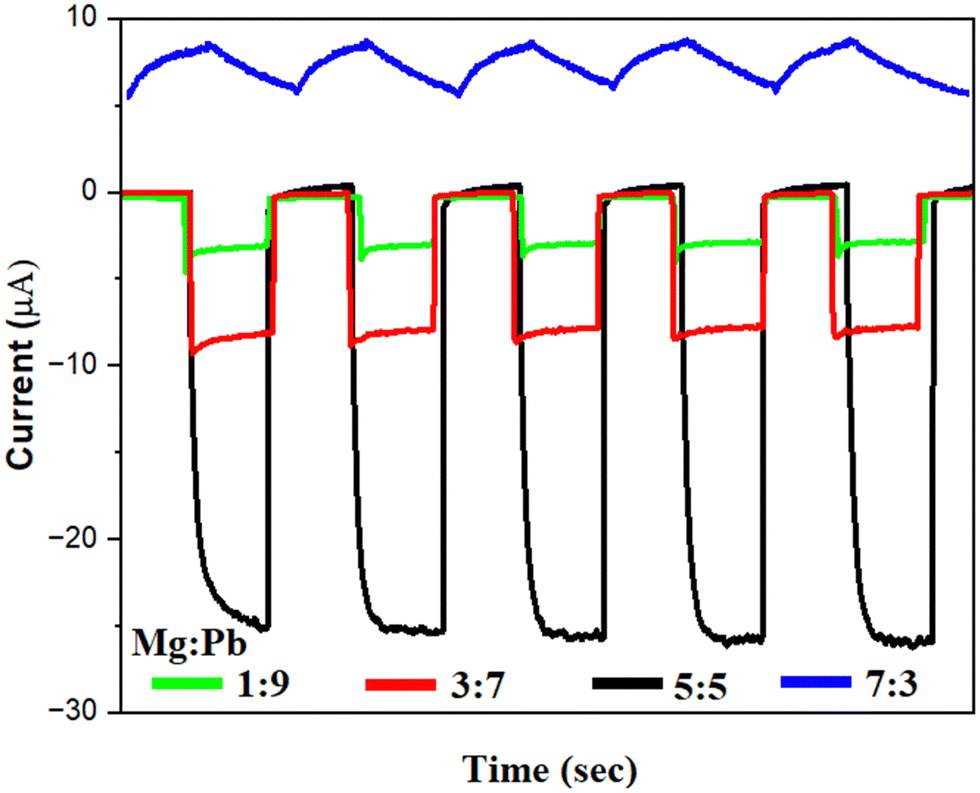 | ||
| Fig. 5 Photodynamic response of devices fabricated with variation in Mg:Pb stoichiometry for samples of Mg:Pb-1:9, Mg:Pb-3:7, Mg:Pb-5:5 and Mg:Pb-7:3. | ||
In summary, the device fabricated from the perovskite film of Mg:Pb-5:5 shows the maximum magnitude of photocurrent, which is attributed to the crystallinity and a favourable bandgap. Henceforth, the Mg:Pb-5:5 device is taken up for the further extensive opto-electronic studies.
I–V characterisation has been performed to reveal the underlying carrier transport behaviour in the photodetector device. Fig. 6a shows the detector I–V characteristics in the voltage range of ±5 V, studied in the dark and under various intensities of simulated solar light. It can be seen that the device follows a non-linear behaviour that is ascribed to the built-in potential at the interface of TiO2 and perovskite.33 It can be further noted that, at the lower voltage range of ±1 V, the current in the device was found to be very low in the range of a few microamps, denoting the presence of a charge-barrier at the interface. However, with the increase in the biasing voltage beyond 1 V, the current in the device rises exponentially, where the potential-barrier in the device is overcome by the biasing and thus the device starts behaving as a normal photoresistor, through ohmic charge transport. Similar, behaviour has been seen when the I–V characterisation is performed at various intensities of light. It should be noted that, even upon the illumination of light, the device retains its inherent charge transport mechanism; however, the magnitude of the current flowing through the device increases with the illumination of light, giving rise to a corresponding change in photocurrent.
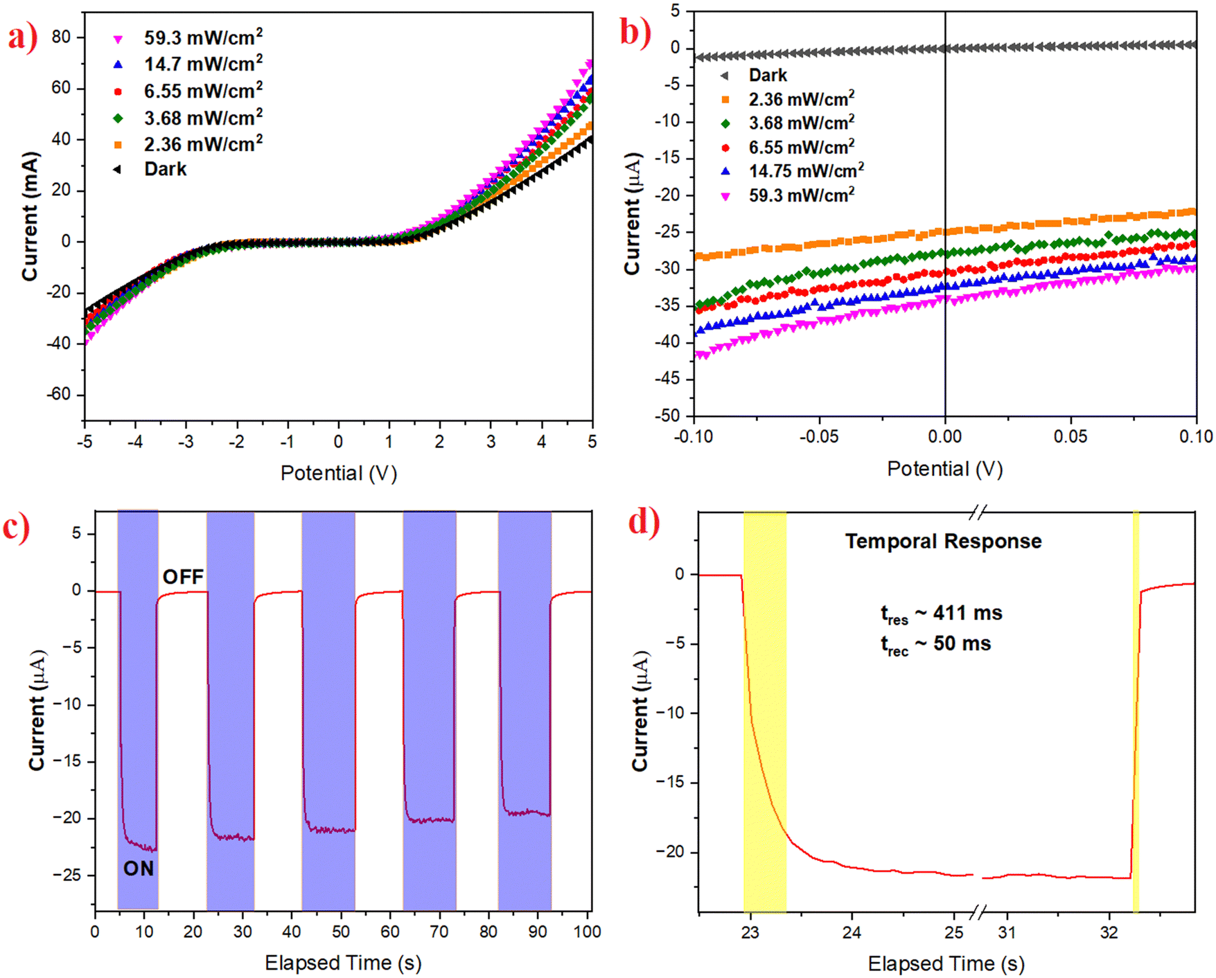 | ||
| Fig. 6 Opto-electronic studies of the device fabricated using Mg:Pb-5:5 film. I–V characteristics of the device under variation of the light intensity and voltage biasing in the range of (a) ±5 V, and (b) ±0.1 V. (c) The photodynamic response of the device under a solar simulator; (d) a single cycle of photodynamic response depicting the response and recovery time. | ||
Furthermore, to clearly demonstrate the self-powered characteristic (zero-bias operation), the I–V characteristics were recorded in an ultra-low bias range of ±0.1 V, as shown in Fig. 6b. The detector shows low dark current at 0 V. When it was illuminated under various intensities, the free charge carriers increased, and thus the device current reached a few microamps. It should be noted that an increase in the current under illumination is also observed at 0 V, thus confirming the capability of the detector to operate without any applied bias.
Further photodynamic studies were performed to determine the response time and recovery time of the photodetector. Response time is the time elapsed by the detector to reach 90% of the saturated photocurrent from 10% of its initial dark current state.34 Similarly, the recovery time is defined as the time taken by the detector to reach back to the initial 10% of its dark current from 90% of its saturated photocurrent.35,36 Response and recovery time are the key parameters to assess how fast the detector responds to incident light input. Fig. 6c depicts the photo-dynamic response over several cycles and it is seen that the response is stable over several cycles, with minimal deviation in the magnitude of the photocurrent. The response and recovery times are estimated to be 411 ms and 50 ms, as seen in Fig. 6d.
3.4 Figures of merit
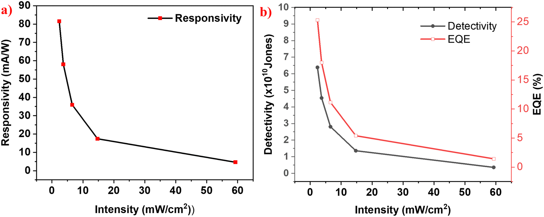
Figures of merit are the key parameters that are employed to assess and compare the performance of photodetector devices. Responsivity is the magnitude of photocurrent in the device per unit intensity of the incident light per unit active area of the device.37 Detectivity is the inverse of the noise equivalent power, which denotes the lowest intensity of the incident light that can generate a response in the detector.38 External quantum efficiency is defined as the ratio of number of photons incident on the detector to the number of photoelectrons being collected at the electrons.39 Higher values of EQE indicate that the incident photons are efficiently collected as photoelectrons.All the figures of merit are calculated at 0 V under various intensities of simulated solar light, as seen in Fig. 7a. Accordingly, it shows a peak responsivity of 81 mA W−1 at zero bias, for the intensity of 2.36 mW cm−2. Responsivities of 58.01 mA W−1, 35.9 mA W−1, 17.4 mA W−1 and 4.59 mA W−1 have been obtained for intensities of 3.68 mW cm−2, 6.55 mW cm−2, 14.75 mW cm−2 and 59.3 mW cm−2, respectively. As shown in Fig. 7b, the detector shows the highest detectivity and EQE values of around 6.5 × 10¹⁰ Jones and 25%, respectively, for the minimal incident light intensity of 2.36 mW cm−2. It is to be noted that all the figures-of-merit display an increase with a decrease in the light intensity and the increment is exponentially varying. This can be attributed to the presence of trap states in the photoactive layers.32,40
 | ||
| Fig. 7 Variation of (a) responsivity and (b) detectivity and EQE with the intensity of simulated solar light for the optimized sample of Mg:Pb-5:5. | ||
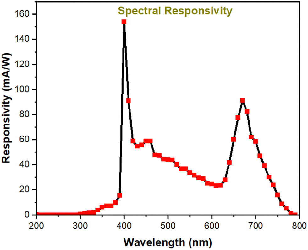
Responsivity and response-recovery times, being the key parameters, so-far estimated are based on the response of the device towards simulated solar light. The simulated solar light consists of a broad wavelength spectrum 200–1100 nm, which doesn’t indicate any idea about the wavelength dependent performance of the device. Hence, to reveal the wavelength-specific performance, the detector is illuminated with monochromatic wavelengths ranging from 200 nm to 800 nm with an increment of 10 nm and the corresponding photocurrent in the detector is recorded, as seen in Fig. 8. The detector shows a broadband response ranging from 350 nm to 780 nm. It should be noted that the device shows higher spectral responsivity of 153 mA W−1 and 91 mA W−1 at 400 nm and 670 nm, respectively. The obtained spectral response is along similar lines as the absorption spectra, where the maximum absorption and maximum spectral response are observed at 400 nm. Furthermore, it is noted that there is also a response peak centered at 680 nm. However in comparison with the response at 400 nm and 680 nm, the response towards the 400–600 nm range is comparatively less. This distinctive spectral response curve can be explained based on the spatial absorption of the incident photons within the absorber layer. As seen in the ESI† (Fig. S2), the TiO2 ETL layer employed in the device displays absorption in the range of 300–340 nm. FTO and TiO2 are highly transparent in the range of 400–800 nm. Hence, it can be asserted that the device response in the range of 400–800 nm is completely associated with the perovskite layer. As mentioned earlier, the light is illuminated from the FTO glass side, with subsequent layers being TiO2, perovskite and the carbon electrode. Photons ranging from 400–800 nm are illuminated upon the device. The point (or layer) at which the photons get absorbed in the device is dictated by the penetration depth of the photon in the perovskite material. Typically, it is well-known that the photons with higher energy will have low penetration depth and get absorbed at lesser thickness in the optical path. Hence higher energy photons (400–450 nm) are expected to get absorbed near the surface of the perovskite. Since, the surface of the perovskite layer is near to the TiO2 layer, the built-in field present near the junction will readily separate the excitons and result in enhanced photocurrent. Similarly, photons in the range of 450–600 nm, due to their comparatively higher penetration depth, are expected to get absorbed in the middle of the perovskite layer, where the electrode interfaces are far and hence the collection probability of the generated charge carriers is very poor. This results in diminished photocurrent in the device towards 450–600 nm. Contrastingly, photons in the range of 600–800 nm, due to their low energy, have very high penetration depth, and hence they are absorbed in the far end of the perovskite layer, which is in close proximity with the carbon electrode. Hence, the photocarriers generated by 600–800 nm photons are efficiently separated and collected, resulting in increased photocurrent.
 | ||
| Fig. 8 Wavelength dependent responsivity of the detector of the optimized sample of Mg:Pb-5:5. | ||
To be concise, since photons in the range of 400–450 nm and 600–800 nm are absorbed near the TiO2-perovskite interface and carbon-perovskite interface, respectively, the charge separation and collection are efficient, resulting in higher photocurrent. However in the case of 450–600 nm photons, the point of charge carrier generation is far away from the perovskite–carbon and perovskite–TiO2 interface, leading to poor charge carrier collection. For the sake of clarity, the above discussion is pictorially represented in Fig. S3 (ESI†).
Photodetectors find applications in several areas such as image sensing, ambient light monitoring, spectroscopy, optical smoke detectors, autonomous driving, medical imaging, barcode scanning, single photon detection, fibre communication, laser range finding, particle counters, remote sensing, etc.41–43 Each specific application has its own minimum required figures-of-merit values. Applications such as visible image sensing, medical imaging and spectroscopy require photodetectors with response in the UV and visible range with very high responsivity and response time in the range of ns to ms.44,45 Applications such as fibre communication, heterodyne measurements and mode beat monitoring, require detectors with ultra-fast response time in the range of a few ps.
Given the scenario, our fabricated photodetector with a responsivity of few mA W−1 and response time of 411 ms, sensitive to the UV-Vis-NIR spectrum, will be useful for applications such as optical smoke detectors, ambient light sensors and optical power meters.
3.5 Device mechanism
The photoexcited charge transport mechanism and device operation are clearly illustrated with the aid of a band diagram. Fig. 9 shows the band diagram of the device, where FTO, m-TiO2, MAPb0.5Mg0.5X3 and carbon act as the photoanode, electron transport layer, photo absorber and photocathode, respectively. Mesoporous titania is chosen as the ETL, as it has suitable band energetics for the efficient transfer of photogenerated electrons from the perovskite.33 FTO is a degenerately doped transparent conducting oxide, which has a Fermi level, favourable for carrier collection from the TiO2.46 Carbon is used as a photocathode and facilitates the transfer of holes from the perovskite as per the relative band levels. The energy gap of MAPb0.5Mg0.5Cl2I is calculated to be 1.55 eV from the absorption studies. Pristine MAPbI3 perovskite has energy levels of 3.9 eV (VB-valence band) and 5.4 eV (CB-conduction band). It is worth mentioning that with the introduction of a dopant atom into the host lattice, the electronic structure and hence energy levels alter and the conduction and valence bands show a shift. Hayase et al. found that with the doping of Mg ions in MAPbI3, the band levels shifted by a minimal magnitude of ±0.11 eV.19 Despite the slight change in the energy levels, the doped-perovskite still forms a type-II heterojunction with the TiO2 electron transport layer, due to the favourable energy band levels. Analogous in our case, the synthesized MAPb0.5Mg0.5Cl2I perovskite is also expected to form a type-II heterojunction with a TiO2 layer. The formation of a type-II heterojunction between te perovskite and TiO2 layers gives rise to a built-in field in the device, which aids in the photodetection process. When light of a suitable wavelength is incident on the device, the photoactive layer absorbs the incident photons giving rise to excitons. The absorbed photons create excitons, which due to the low excitonic binding energy, are readily dissociated with the aid of the built-in field at the interface.6 Thus, the electrons readily reach the CB of the TiO2. The dissociated photoexcited electrons and holes are collected at the FTO and carbon, respectively, thus giving rise to the photocurrent in the device.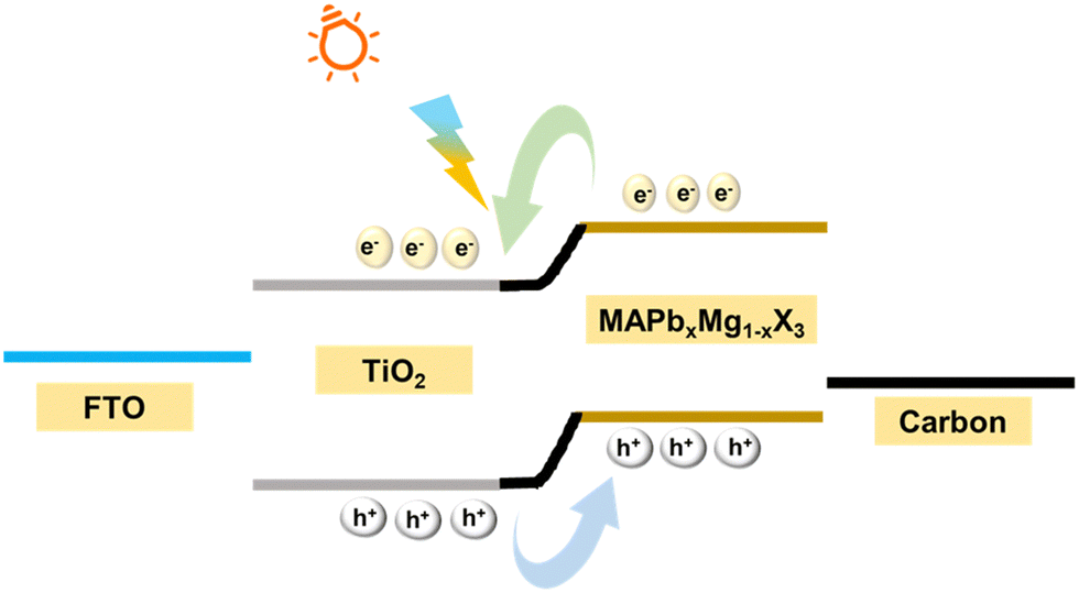 | ||
| Fig. 9 Schematic illustration of the photocarrier transport in the device using the band diagram. | ||
3.6 Stability and reproducibility
For any opto-electronic material to be useful in practical applications, stability is a crucial parameter. Hence, in order to assess the stability of our synthesized perovskite, the fabricated devices were stored in ambient conditions for 48 hours and the photocurrent was measured. And it is seen, the device has shown a negligible difference in the magnitude of the photocurrent. Again the device performance was evaluated after 96 hours, where the decrease in performance was evident, as seen in Fig. S4 (ESI†).In order to confirm the repeatability, device fabrication is repeated and 3 devices are fabricated with the optimized CH3NH3Mg0.5Pb0.5X3 perovskite. Fig. S5 (ESI†) shows the temporal response of the fabricated devices and it is seen that the photocurrent values of 26.13 μA, 23.5 μA and 26.02 μA are obtained. The photocurrent is measured under illumination with light of intensity 2.36 mW cm−2. The deviation in the photocurrent values is minimal and this shows the repeatability of the obtained results.
3.7 Comparison of the MAPb1−xMgxX3 photodetector with other perovskite-based photodetectors
Table 2 compares the performance of the MAPb0.5Mg0.5X3 photodetector with the lead-based and lead-free mixed cation detectors. In a report, a zero-biased photodetector based on MAPbI3 with spiro-OmeTAD as the HTL and TiO2 as the ETL is demonstrated, which shows low responsivity of 16 mA W−1.47 An Ag-doped PEDOT:PSS layer is used as the HTL for a self-powered photodetector based on MAPbI3 as the active layer. Though the device has shown decent responsivity, the inherent acidity of PEDOT:PSS severely hampers the stability of the fabricated detector.50 In another report, ZnO and MoO3 are used as ETL and HTL layers, with MAPbI3 as the active layer. However the device exhibited minimal response of 48 mA W−1.51 Another report has employed Cu-doped MAPbI3 as an active layer for a self-powered photodetector, which shows good responsivity and quicker response times. However, the device fabrication scheme involves complex methodology and the usage of unstable organic ETL layers.52| S. no | Device architecture | Bias (V) | Spectral range | Responsivity (mA W−1) | Res/Rec time (ms) | Remarks | Ref. |
|---|---|---|---|---|---|---|---|
| Lead-based detectors | |||||||
| 1 | C/TiO2/MAPbI3-spiro OMeTAD/Au | 0 | 750 nm | 16.9 | 200/200 | HTL is used/low response | 47 |
| 2 | FTO/MAPbI3 | 0 | 500 nm | 59 | 20/20 | Low response | 48 |
| 3 | FTO/ZnO/MAPI/spiro-OMeTAD/Cu | 0 | 325 nm | 26.7 | 53/63 | Complex architecture | 49 |
| 4 | FTO/PEDOT:PSS + Ag/MAPI/Al | 0 | 400 nm | 250 | 110/72 | Acidic PEDOT:PSS | 50 |
| 5 | FTO/ZnO/MAPI/MoO3/Au | 0 | 380 nm | 48 | 14/12 | HTL is used | 51 |
| 6 | ITO/MAPI:Cu/PCBM/BCP/Ag | 0 | 685 nm | 370 | 0.005/0.005 | Complex architecture | 52 |
| Lead-free or mixed cation based detectors | |||||||
| 7 | Si/MPS-MoO3-PEDOT-MAPbSnI3-PCBM- Zr | −10 mV | 300–1000 | 200 | — | Complex fabrication | 53 |
| 8 | Au-(RNH3)2(CH3NH3)n−1MnX3n+1-Au | 30 | White light | 13 | 10/7.5 ms | Very high bias | 54 |
| 9 | MA3Bi2I9 (FTO/MABI/Ag) | 0 | 300–600 | 1.76 | 26/41 ms | Poor response | 55 |
| 10 | Au-MA3Sb2I9-Au | 5 | 400–750 | 40 × 103 | 0.4/0.9 ms | Single crystal|high bias | 56 |
| 11 | FTO-TiO2-MAMnI3-spiroOmeTAD | 0 | 300–762 | — | ∼1 s | HTL is used | 57 |
| 12 | FTO/TiO2/(CH3NH3)2FeCuI4Cl2/Au | 0.3 | 300–700 | 1.4 × 10⁻² | — | Poor response | 58 |
| 13 | FTO/TiO2/(CH3NH3)2InCuI6/Au | 0.3 | 300–700 | 0.8 | — | Poor response | 58 |
| 14 | Al-MASnI3-Au | 2 | 550–1000 nm | 470 | 1500/400 | CVD high bias | 59 |
| 15 | FTO/TiO 2 /MAPb 0.5 Mg 0.5 X 3 /C | 0 | 400 nm | 153 | 411/50 | This Work | |
| 670 nm | 91 | ||||||
In an effort to completely avert or reduce the lead usage, metal cations such as Sn, Bi, Sb, Mn, Cu, etc. have been employed for photodetection, as shown in Table 2. In a report, a Sn-based MASnI3-based photodetector is fabricated in the photoconductor configuration. Despite showing high responsivity of 470 mA W−1, the device operates at a higher bias of 2 V due to its architecture and sophisticated chemical vapour deposition is employed for film deposition.59 In another report, Bi cation-based MA3Bi2I9 is used for photodetection in an HTL-free configuration, but the device exhibited a poor responsivity of 1.76 mA W−1.55 Furthermore, in a report, Sb cation-based MA2Sb2I9 single crystals were employed for broadband photodetection in a photoconductor architecture. Though the device shows high responsivity of 40 A W−1, the bias voltage is very high in the range of 5 V. Furthermore, the growth of single crystals is a complex and tedious process, which hinders the device fabrication and integration.56 In another report, a Mn cation-based perovskite film is deposited and the formed MAMnI3 film is employed for photodetection. Owing to the poor optical and film formation characteristics of the MAMnI3 perovskite, the device displayed very poor response.57
As seen in the table, our fabricated MAPb0.5Mg0.5X3-based photodetector showed excellent responsivity and response time with a simple HTM-free architecture. Despite the significant reduction in Pb content, the decrement in absorption is very minimal. Thus, these partially Mg-substituted perovskites can be significant for Pb reduction and still retain their inherent properties to a larger extent. The observed figures of merit of our device were comparable to Pb-based devices and superior to Pb-free alternation cation based-devices. The deposited perovskite, despite reducing the Pb content by 50%, displays significant performance. The impressive performance of the detector is ascribed to the excellent opto-electronic properties of the MAPb0.5Mg0.5X3 and built-in field at the junction of the MAPb0.5Mg0.5X3 and TiO2.
Environmental sustainability is an important aspect for the devices to be employed for practical applications. Pb is a well-known neurotoxin, which poses a significant threat for health and its commercialization in the market. Lead, being a heavy metal ion and due to its solubility with water, is of concern regarding the contamination of the surrounding environment. This 50% substitution of Pb with Mg significantly aids in the reduction of the Pb footprint in the devices. Apart from the Pb toxicity, another important concern in the perovskite devices is the usage of noble metals as top electrodes, which involves costly and unsustainable mining and refinement processes. It should be noted that our device employed an HTM-free architecture and noble metal-free carbon electrode, which makes the fabrication of the device much easier and cost-effective. However, most of the listed photodetectors have employed both electron transport and hole transport layers, besides using metal electrodes. As per a life cycle assessment study, gold production is of the largest environmental concern for perovskite solar cell systems.60 The substitution of a much more environmentally benign material for gold can significantly reduce the total environmental impact. Carbon paste as a top electrode drastically reduces production energy requirements and impacts on the environment. Nonetheless, limitations with our device such as ambient stability and slightly higher response time range in milliseconds need to be well analysed and addressed in future studies.
4. Conclusion
In summary, we report the synthesis of a Mg-substituted perovskite photodetector using a simple and facile solution processed technique. A broadband, self-driven photodetector has been demonstrated using the optimized perovskite of MAPb0.5Mg0.5Cl2I. The photodetector shows an excellent response of 153 mA W−1 and response/recovery time of 411/50 ms at zero bias (self-powered) and broadband UV-Vis response as well. The facile synthesis enabled device fabrication with a simple architecture (organic HTM and metal cathode free), and this work could pave the way to 50% reduced toxic Pb2+ cation in the opto-electronic device that works by self-power design, making it a suitable contribution for energy conservation.Author contributions
Kumaar Swamy Reddy B.: conceptualization, methodology, validation, visualization, writing – original draft. Smruti Panda: conceptualization, methodology, validation, visualization, writing – original draft. Ganapathy Veerappan: conceptualization, supervision, data curation, formal analysis, methodology, validation, visualization, funding acquisition, resources, writing – review & editing. Easwaramoorthi Ramasamy: data curation, formal analysis, funding acquisition. Sushmee Badhulika: supervision, data curation, formal analysis, writing – review & editing. Pramod H. Borse: conceptualization, methodology, funding acquisition, investigation, resources, supervision, writing – review & editing.Conflicts of interest
The authors declare that they have no known competing financial interests or personal relationships that could have appeared to influence the work reported in this paper.Acknowledgements
VG acknowledges the Department of Science and Technology, New Delhi, India, for financial support through TRC (AI/1/65/ARCI/2014) and SERB Research Scientist (SB/SRS/2019-20/22PS). The authors (KSRB and SP) extend their acknowledgment to the Director, ARCI (DST, India lab) for financial support and providing all experimental facilities at ARCI. SB acknowledges the financial assistance from the Defence Research and Development Organisation (DRDO) grant DYSL-AST/CARS/CONTRACT/20-21/02.References
- C. Li, H. Wang, F. Wang, T. Li, M. Xu, H. Wang, Z. Wang, X. Zhan, W. Hu and L. Shen, Ultrafast and Broadband Photodetectors Based on a Perovskite/Organic Bulk Heterojunction for Large-Dynamic-Range Imaging, Light: Science & Applications, 2020, 9(1), 31, DOI:10.1038/s41377-020-0264-5.
- T. Hellmann, C. Das, T. Abzieher, J. A. Schwenzer, M. Wussler, R. Dachauer, U. W. Paetzold, W. Jaegermann and T. Mayer, The Electronic Structure of MAPI-Based Perovskite Solar Cells: Detailed Band Diagram Determination by Photoemission Spectroscopy Comparing Classical and Inverted Device Stacks, Adv. Energy Mater., 2020, 10(42), 2002129, DOI:10.1002/aenm.202002129.
- E. Mosconi, P. Umari and F. De Angelis, Electronic and Optical Properties of MAPbX3 Perovskites (X = I, Br, Cl): A Unified DFT and GW Theoretical Analysis, Phys. Chem. Chem. Phys., 2016, 18(39), 27158–27164, 10.1039/C6CP03969C.
- T.-B. Song, Q. Chen, H. Zhou, C. Jiang, H.-H. Wang, Y. (Michael) Yang, Y. Liu, J. You and Y. Yang, Perovskite Solar Cells: Film Formation and Properties, J. Mater. Chem. A, 2015, 3(17), 9032–9050, 10.1039/C4TA05246C.
- A. M. A. Leguy, P. Azarhoosh, M. Isabel Alonso, J. Campoy-Quiles, O. Weber, J. Yao, D. Bryant, M. Weller, J. Nelson, A. Walsh, M. van Schilfgaarde and P. R. Barnes, Experimental and Theoretical Optical Properties of Methylammonium Lead Halide Perovskites, Nanoscale, 2016, 8(12), 6317–6327, 10.1039/C5NR05435D.
- M. Baranowski and P. Plochocka, Excitons in Metal-Halide Perovskites, Adv. Energy Mater., 2020, 10(26), 1903659, DOI:10.1002/aenm.201903659.
- C. Motta, F. El-Mellouhi and S. Sanvito, Charge Carrier Mobility in Hybrid Halide Perovskites, Sci. Rep., 2015, 5(1), 12746, DOI:10.1038/srep12746.
- High Charge Carrier Mobilities and Lifetimes in Organolead Trihalide Perovskites - Wehrenfennig-2014-Advanced Materials-Wiley Online Library. https://onlinelibrary.wiley.com/doi/full/10.1002/adma.201305172 (accessed 2023-04-26).
- S. S. Dipta and A. Uddin, Stability Issues of Perovskite Solar Cells: A Critical Review, Energy Technol., 2021, 9(11), 2100560, DOI:10.1002/ente.202100560.
- M. Wang, W. Wang, B. Ma, W. Shen, L. Liu, K. Cao, S. Chen and W. Huang, Lead-Free Perovskite Materials for Solar Cells, Nano-Micro Lett., 2021, 13(1), 62, DOI:10.1007/s40820-020-00578-z.
- A. E. Shalan, S. Kazim and S. Ahmad, Lead-Free Perovskites: Metals Substitution towards Environmentally Benign Solar Cell Fabrication, ChemSusChem, 2019, 12(18), 4116–4139, DOI:10.1002/cssc.201901296.
- T. Nakamura, T. Handa, R. Murdey, Y. Kanemitsu and A. Wakamiya, Materials Chemistry Approach for Efficient Lead-Free Tin Halide Perovskite Solar Cells, ACS Appl. Electron. Mater., 2020, 2(12), 3794–3804, DOI:10.1021/acsaelm.0c00859.
- Y. Ogomi, A. Morita, S. Tsukamoto, T. Saitho, N. Fujikawa, Q. Shen, T. Toyoda, K. Yoshino, S. S. Pandey, T. Ma and S. Hayase, CH3NH3SnxPb(1–x)I3 Perovskite Solar Cells Covering up to 1060 Nm, J. Phys. Chem. Lett., 2014, 5(6), 1004–1011, DOI:10.1021/jz5002117.
- T. Mahmoudi, W.-Y. Rho, M. Kohan, Y. H. Im, S. Mathur and Y.-B. Hahn, Suppression of Sn2 +/Sn4+ Oxidation in Tin-Based Perovskite Solar Cells with Graphene-Tin Quantum Dots Composites in Active Layer, Nano Energy, 2021, 90, 106495, DOI:10.1016/j.nanoen.2021.106495.
- X.-G. Zhao, J.-H. Yang, Y. Fu, D. Yang, Q. Xu, L. Yu, S.-H. Wei and L. Zhang, Design of Lead-Free Inorganic Halide Perovskites for Solar Cells via Cation-Transmutation, J. Am. Chem. Soc., 2017, 139(7), 2630–2638, DOI:10.1021/jacs.6b09645.
- D. Ray, C. Clark, H. Q. Pham, J. Borycz, R. J. Holmes, E. S. Aydil and L. Gagliardi, Computational Study of Structural and Electronic Properties of Lead-Free CsMI3 Perovskites (M = Ge, Sn, Pb, Mg, Ca, Sr, and Ba), J. Phys. Chem. C, 2018, 122(14), 7838–7848, DOI:10.1021/acs.jpcc.8b00226.
- Y. D. Zhang and J. Feng, CH3NH3Pb1−xMgxI3 Perovskites as Environmentally Friendly Photovoltaic Materials, AIP Adv., 2018, 8(1), 015218, DOI:10.1063/1.5006241.
- C. Tablero Crespo, Effect of Substitution of Pb for Mg on the Photovoltaic Properties of Methyl-Ammonium Lead Iodide Perovskites, Adv. Theory Simul., 2022, 5(3), 2100509, DOI:10.1002/adts.202100509.
- F. Yang, M. A. Kamarudin, G. Kapil, D. Hirotani, P. Zhang, C. H. Ng, T. Ma and S. Hayase, Magnesium-Doped MAPbI3 Perovskite Layers for Enhanced Photovoltaic Performance in Humid Air Atmosphere, ACS Appl. Mater. Interfaces, 2018, 10(29), 24543–24548, DOI:10.1021/acsami.8b06619.
- P. Singh, P. J. S. Rana, R. Mukherjee and P. Srivastava, A Step towards Environmental Benign Mg/Pb Based Binary Metal Mixed Halide Perovskite Material, Sol. Energy, 2018, 170, 769–779, DOI:10.1016/j.solener.2018.05.090.
- M. Sulaman, S. Yang, A. Imran, Z. Zhang, A. Bukhtiar, Z. Ge, Y. Song, F. Sun, Y. Jiang, L. Tang and B. Zou, Two Bulk-Heterojunctions Made of Blended Hybrid Nanocomposites for High-Performance Broadband, Self-Driven Photodetectors, ACS Appl. Mater. Interfaces, 2023, 15(21), 25671–25683, DOI:10.1021/acsami.3c01749.
- M. Sulaman, S. Y. Yang, Z. H. Zhang, A. Imran, A. Bukhtiar, Z. H. Ge, Y. Tang, Y. R. Jiang, L. B. Tang and B. S. Zou, Lead-Free Tin-Based Perovskites Nanocrystals for High-Performance Self-Driven Bulk-Heterojunction Photodetectors, Mater. Today Phys., 2022, 27, 100829, DOI:10.1016/j.mtphys.2022.100829.
- S. Supraja, K. R. Dileep, N. Chundi, E. Ramasamy, S. Shanmugasundaram and G. Veerappan, Influence of Bi-Phasic TiO2 as a Low-Temperature Curable Electron Transport Layer for Efficient Perovskite Solar Cells, Sol. Energy, 2022, 247, 308–314, DOI:10.1016/j.solener.2022.10.037.
- S. Maniarasu, V. Karthikeyan, T. B. Korukonda, S. C. Pradhan, S. Soman, E. Ramasamy and G. Veerappan, Ambient Processed Perovskite Sensitized Porous TiO2 Nanorods for Highly Efficient and Stable Perovskite Solar Cells, J. Alloys Compd., 2021, 884, 161061, DOI:10.1016/j.jallcom.2021.161061.
- P. S. Whitfield, N. Herron, W. E. Guise, K. Page, Y. Q. Cheng, I. Milas and M. K. Crawford, Structures, Phase Transitions and Tricritical Behavior of the Hybrid Perovskite Methyl Ammonium Lead Iodide, Sci. Rep., 2016, 6(1), 35685, DOI:10.1038/srep35685.
- Z. Siddique, J. L. Payne, J. T. S. Irvine, L. K. Jagadamma, Z. Akhter, I. D. W. Samuel and A. Iqbal, Effect of Halide-Mixing on Tolerance Factor and Charge-Carrier Dynamics in (CH3NH3PbBr3−xClx) Perovskites Powders, J. Mater. Sci.: Mater. Electron., 2020, 31(21), 19415–19428, DOI:10.1007/s10854-020-04475-4.
- J. Navas, A. Sánchez-Coronilla, J. J. Gallardo, N. Cruz Hernández, J. C. Piñero, R. Alcántara, C. Fernández-Lorenzo, D. M. De los Santos, T. Aguilar and J. Martín-Calleja, New Insights into Organic–Inorganic Hybrid Perovskite CH3NH3PbI3 Nanoparticles. An Experimental and Theoretical Study of Doping in Pb2+ Sites with Sn2 +, Sr2 +, Cd2+ and Ca2+, Nanoscale, 2015, 7(14), 6216–6229, 10.1039/C5NR00041F.
- M. D. Sampson, J. S. Park, R. D. Schaller, M. K. Y. Chan and A. B. F. Martinson, Transition Metal-Substituted Lead Halide Perovskite Absorbers, J. Mater. Chem. A, 2017, 5(7), 3578–3588, 10.1039/C6TA09745F.
- J. H. Heo and S. H. Im, Highly Reproducible, Efficient Hysteresis-Less CH3NH3PbI3−xClx Planar Hybrid Solar Cells without Requiring Heat-Treatment, Nanoscale, 2016, 8(5), 2554–2560, 10.1039/C5NR08458J.
- S. Yakunin, D. Dirin, Y. Shynkarenko, V. Morad, I. Cherniuh, O. Nazarenko, D. Kreil, T. Nauser and M. Kovalenko, Detection of Gamma Photons Using Solution-Grown Single Crystals of Hybrid Lead Halide Perovskites, Nat. Photonics, 2016, 10, DOI:10.1038/nphoton.2016.139.
- H.-A. Chen, M.-H. Lee and C.-W. Chen, Wavelength-Dependent Optical Transition Mechanisms for Light-Harvesting of Perovskite MAPbI3 Solar Cells Using First-Principles Calculations, J. Mater. Chem. C, 2016, 4(23), 5248–5254, 10.1039/C6TC00773B.
- K. S. Reddy B, S. Veeralingam, P. H. Borse and S. Badhulika, High Responsivity Self-Powered Flexible Broadband Photodetector Based on Hybrid Selenium-PEDOT:PSS Junction, Org. Electron., 2022, 108, 106586, DOI:10.1016/j.orgel.2022.106586.
- B. C. O’Regan, P. R. F. Barnes, X. Li, C. Law, E. Palomares and J. M. Marin-Beloqui, Optoelectronic Studies of Methylammonium Lead Iodide Perovskite Solar Cells with Mesoporous TiO2: Separation of Electronic and Chemical Charge Storage, Understanding Two Recombination Lifetimes, and the Evolution of Band Offsets during J–V Hysteresis, J. Am. Chem. Soc., 2015, 137(15), 5087–5099, DOI:10.1021/jacs.5b00761.
- Z. Shuang, H. Zhou, D. Wu, X. Zhang, B. Xiao, G. Ma, J. Zhang and H. Wang, Low-Temperature Process for Self-Powered Lead-Free Cs2AgBiBr6 Perovskite Photodetector with High Detectivity, Chem. Eng. J., 2022, 433, 134544, DOI:10.1016/j.cej.2022.134544.
- D. Wu, Y. Xu, H. Zhou, X. Feng, J. Zhang, X. Pan, Z. Gao, R. Wang, G. Ma, L. Tao, H. Wang, J. Duan, H. Wan, J. Zhang, L. Shen, H. Wang and T. Zhai, Ultrasensitive, Flexible Perovskite Nanowire Photodetectors with Long-Term Stability Exceeding 5000 h, InfoMat, 2022, 4(9), e12320, DOI:10.1002/inf2.12320.
- Z. Gao, H. Zhou, K. Dong, C. Wang, J. Wei, Z. Li, J. Li, Y. Liu, J. Zhao and G. Fang, Defect Passivation on Lead-Free CsSnI3 Perovskite Nanowires Enables High-Performance Photodetectors with Ultra-High Stability, Nano-Micro Lett., 2022, 14(1), 215, DOI:10.1007/s40820-022-00964-9.
- K. S. Reddy B, S. Veeralingam, P. H. Borse and S. Badhulika, 1D NiO–3D Fe2O3 Mixed Dimensional Heterostructure for Fast Response Flexible Broadband Photodetector, Nanotechnology, 2022, 33(23), 235201, DOI:10.1088/1361-6528/ac5838.
- S. Veeralingam and S. Badhulika, Enhanced Carrier Separation Assisted High-Performance Piezo-Phototronic Self-Powered Photodetector Based on Core-Shell ZnSnO3 @In2O3 Heterojunction, Nano Energy, 2022, 98, 107354, DOI:10.1016/j.nanoen.2022.107354.
- B. Kumaar Swamy Reddy, S. Veeralingam, P. H. Borse and S. Badhulika, A Flexible, Rapid Response, Hybrid Inorganic–Organic SnSe2–PEDOT:PSS Bulk Heterojunction Based High-Performance Broadband Photodetector, Mater. Chem. Front., 2022, 6(3), 341–351, 10.1039/D1QM01232K.
- M. I. Saleem, M. Sulaman, A. Batool, A. Bukhtiar and S. Khalid, Suppression of Mid-Gap Trap State in CsPbBr3 Nanocrystals with Br-Passivation for Self-Powered Photodetector, Energy Technol., 2023, 11(7), 2300013, DOI:10.1002/ente.202300013.
- M. Usman, S. Nisar, D. Kim, S. Golovynskyi, M. Imran, G. Dastgeer and L. Wang, Polarization-Sensitive Photodetection of Anisotropic 2D Black Arsenic, J. Phys. Chem. C, 2023, 127(19), 9076–9082, DOI:10.1021/acs.jpcc.2c08630.
- S. Shafique, S. Yang, Y. T. Woldu and Y. Wang, Hierarchical Synthesis of Urchin-like V2O5 Hollow Spheres and Its Photodetection Properties, Sens. Actuators, A, 2019, 288, 107–116, DOI:10.1016/j.sna.2019.01.029.
- S. Shafique, S. Yang, Y. Wang, Y. T. Woldu, B. Cheng and P. Ji, High-Performance Photodetector Using Urchin-like Hollow Spheres of Vanadium Pentoxide Network Device, Sens. Actuators, A, 2019, 296, 38–44, DOI:10.1016/j.sna.2019.07.003.
- A. Imran, Q. Zhu, M. Sulaman, A. Bukhtiar and M. Xu, Electric-Dipole Gated Two Terminal Phototransistor for Charge-Coupled Device, Adv. Opt. Mater., 2023, 2300910, DOI:10.1002/adom.202300910.
- M. Qasim, M. Sulaman, A. Bukhtiar, B. Deng, A. Jalal, Y. Sandali, N. H. Shah, C. Li, G. Dastgeer and H. Bin, High-Performance Self-Powered Broadband Schottky Junction Photodetector Based on Graphene-Silicon van der Waals Heterostructure, Energy Technology, 2023, 2300492, DOI:10.1002/ente.202300492.
- S. Rühle and T. Dittrich, Investigation of the Electric Field in TiO2/FTO Junctions Used in Dye-Sensitized Solar Cells by Photocurrent Transients, J. Phys. Chem. B, 2005, 109(19), 9522–9526, DOI:10.1021/jp046211y.
- H. Sun, T. Lei, W. Tian, F. Cao, J. Xiong and L. Li, Self-Powered, Flexible, and Solution-Processable Perovskite Photodetector Based on Low-Cost Carbon Cloth, Small, 2017, 13(28), 1701042, DOI:10.1002/smll.201701042.
- A. Popoola, M. A. Gondal, I. K. Popoola and L. E. Oloore, Self-Driven, Quadridirectional Carrier Transport, Bifacial MAPbI3–Perovskites Photodiodes Fabricated via Laterally Aligned Interconnected Sandwiched Type Architecture, ACS Appl. Electron. Mater., 2020, 2(8), 2479–2488, DOI:10.1021/acsaelm.0c00417.
- Z. Wang, R. Yu, C. Pan, Z. Li, J. Yang, F. Yi and Z. L. Wang, Light-Induced Pyroelectric Effect as an Effective Approach for Ultrafast Ultraviolet Nanosensing, Nat. Commun., 2015, 6(1), 8401, DOI:10.1038/ncomms9401.
- J. Ghosh, G. Natu and P. K. Giri, Plasmonic Hole-Transport-Layer Enabled Self-Powered Hybrid Perovskite Photodetector Using a Modified Perovskite Deposition Method in Ambient Air, Org. Electron., 2019, 71, 175–184, DOI:10.1016/j.orgel.2019.05.021.
- J. Yu, X. Chen, Y. Wang, H. Zhou, M. Xue, Y. Xu, Z. Li, C. Ye, J. Zhang, P. A. van Aken, P. D. Lund and H. Wang, A High-Performance Self-Powered Broadband Photodetector Based on a CH3NH3PbI3 Perovskite/ZnO Nanorod Array Heterostructure, J. Mater. Chem. C, 2016, 4(30), 7302–7308, 10.1039/C6TC02097F.
- Z. Liu, X. Liu, B. Sun, X. Tan, H. Ye, J. Zhou, Z. Tang, T. Shi and G. Liao, A Cu-Doping Strategy to Enhance Photoelectric Performance of Self-Powered Hole-Conductor-Free Perovskite Photodetector for Optical Communication Applications, Adv. Mater. Technol., 2020, 5(8), 2000260, DOI:10.1002/admt.202000260.
- H. L. Zhu, H. Lin, Z. Song, Z. Wang, F. Ye, H. Zhang, W.-J. Yin, Y. Yan and W. C. H. Choy, Achieving High-Quality Sn–Pb Perovskite Films on Complementary Metal-Oxide-Semiconductor-Compatible Metal/Silicon Substrates for Efficient Imaging Array, ACS Nano, 2019, 13(10), 11800–11808, DOI:10.1021/acsnano.9b05774.
- J. Zhou, Y. Chu and J. Huang, Photodetectors Based on Two-Dimensional Layer-Structured Hybrid Lead Iodide Perovskite Semiconductors, ACS Appl. Mater. Interfaces, 2016, 8(39), 25660–25666, DOI:10.1021/acsami.6b09489.
- A. A. Hussain, A. K. Rana and M. Ranjan, Air-Stable Lead-Free Hybrid Perovskite Employing Self-Powered Photodetection with an Electron/Hole-Conductor-Free Device Geometry, Nanoscale, 2019, 11(3), 1217–1227, 10.1039/C8NR08959K.
- B. Yang, Y.-J. Li, Y.-X. Tang, X. Mao, C. Luo, M.-S. Wang, W.-Q. Deng and K.-L. Han, Constructing Sensitive and Fast Lead-Free Single-Crystalline Perovskite Photodetectors, J. Phys. Chem. Lett., 2018, 9(11), 3087–3092, DOI:10.1021/acs.jpclett.8b01116.
- X. Zhang, J. Yin, Z. Nie, Q. Zhang, N. Sui, B. Chen, Y. Zhang, K. Qu, J. Zhao and H. Zhou, Lead-Free and Amorphous Organic–Inorganic Hybrid Materials for Photovoltaic Applications: Mesoscopic CH3NH3MnI3/TiO2 Heterojunction, RSC Adv., 2017, 7(59), 37419–37425, 10.1039/C7RA04235C.
- S. Tao, Y. Chen, J. Cui, H. Zhou, N. Yu, X. Gao, S. Cui, C. Yuan, M. Liu, M. Wang, X. Wang, H. Gong, Y. Li, T. Liu, X. Sun, J. Yin, X. Zhang and M. Wu, Organic–Inorganic Hybrid (CH3NH3)2FeCuI4Cl2 and (CH3NH3)2InCuI6 for Ultraviolet Light Photodetectors, Chem. Commun., 2020, 56(12), 1875–1878, 10.1039/C9CC09408C.
- A. Waleed, M. M. Tavakoli, L. Gu, Z. Wang, D. Zhang, A. Manikandan, Q. Zhang, R. Zhang, Y.-L. Chueh and Z. Fan, Lead-Free Perovskite Nanowire Array Photodetectors with Drastically Improved Stability in Nanoengineering Templates, Nano Lett., 2017, 17(1), 523–530, DOI:10.1021/acs.nanolett.6b04587.
- K. P. Goetz, A. D. Taylor, Y. J. Hofstetter and Y. Vaynzof, Sustainability in Perovskite Solar Cells, ACS Appl. Mater. Interfaces, 2021, 13(1), 1–17, DOI:10.1021/acsami.0c17269.
Footnotes |
| † Electronic supplementary information (ESI) available: I–V characteristics of devices fabricated with various ratios of Mg:Pb; formulae for the calculation of the figures-of-merit; optical absorption of the TiO2 ETL; schematic explaining the optical pathway of the illuminated photons and their spatial absorption in the device. See DOI: https://doi.org/10.1039/d3ma00411b |
| ‡ Sushmee Badhulika coordinated the research work at IIT, Hyderabad India. |
| § Veerappan Ganapathy contributed the work on the perovskite system in ARCI, Hyderabad India. |
| This journal is © The Royal Society of Chemistry 2023 |