
 Open Access Article
 This Open Access Article is licensed under a
 Creative Commons Attribution 3.0 Unported Licence
Amorphous N-doped InSnZnO thin films deposited by RF sputtering for thin-film transistor application
Zhi-Yue
Li
 abc,
Shu-Mei
Song
a,
Wanxia
Wang
*d,
Ming-Jiang
Dai
e,
Song-Sheng
Lin
e,
Ting-Yong
Chen
b and
Hui
Sun
*a
abc,
Shu-Mei
Song
a,
Wanxia
Wang
*d,
Ming-Jiang
Dai
e,
Song-Sheng
Lin
e,
Ting-Yong
Chen
b and
Hui
Sun
*a
aSchool of Space Science and Physics, Shandong University, Weihai, 264209, China. E-mail: sunhuichn@hotmail.com; Tel: +86-15615816261
bShenzhen Institute for Quantum Science and Engineering, Southern University of Science and Technology, Shenzhen, 518055, China
cDepartment of Physics, The University of Hong Kong, Hong Kong, 999077, China
dSchool of Mechanical, Electrical and Information Engineering, Shandong University, Weihai, 264200, China. E-mail: wang_wanxia@sdu.edu.cn
eGuangdong Institute of New Materials, 363 Changxing Road, Guangzhou, 510651, China
First published on 31st October 2023
Abstract
N-doped InSnZnO (ITZO:N) thin films as the active layer of thin film transistors (TFTs) were prepared using radio frequency (RF) magnetron sputtering at room temperature. The influence of RF power on the microstructure and optical properties of films was investigated. The relationship between the active layer quality and the TFT's electrical properties was also studied. The results show that no evident impacts of RF power are observed on the optical transmittance in the visible range of amorphous ITZO:N thin films. Their optical band gaps increase from 3.44 to 3.54 eV. An appropriate RF power can enhance ITZO:N film's quality, and reduce the interface state density, which is beneficial to improving the carrier concentration of ITZO:N TFTs. Then, the device's performance is optimized. The threshold voltage of TFTs shows a negative shift as the RF power gradually increases. When the RF power is 60 W, the ITZO:N thin film is amorphous with a dense microstructure. The corresponding TFT device exhibits optimal electrical characteristics. Its field-effect mobility, on/off ratio and subthreshold swing are 14.66 cm2 V−1 s−1, >106 and 0.7 V dec−1, respectively.
1. Introduction
Since ZnO thin film transistors (TFTs) prepared by radio frequency (RF) magnetron sputtering at room temperature have been reported by Fortunato and Martins et al. in 2004,1 TFTs with ZnO-based thin films as the active layer have drawn much attention by researchers. Many studies have confirmed that ZnO films doped with Ga,2 Al,3 In,4–6 Sn7,8 or other elements9–11 possess good uniformity and low resistivity, which are suitable for their applications in optoelectronic fields such as flat panel displays. Among these ZnO-based materials, InSnZnO (ITZO) composed of In2O3, SnO2 and ZnO is advantageous due to its wide bandgap (>3.2 eV) and high transmittance (>85%) in the visible light region.12–16 The bottom of its conduction band mainly consisted of In5s and Sn5s orbitals that have strong divergence and high symmetry, which favors electron mobility.17,18 In addition, the substitution of two In3+ ions by the Zn2+/Sn4+ impurity pair results in lattice distortion and contributes to the formation of defects such as oxygen vacancies and (SnIn)˙. This would induce extra free electrons and thus increase the carrier concentration.19,20 Under these conditions, the film's electrical properties are obviously strengthened. However, for most ZnO-based TFTs, the adsorption of gas molecules, such as O2, at the back-channel position will capture the electrons, while their desorption will result in electron release in the film.3,21 This behavior leads to the instability of the TFT's electrical properties. This is a major issue in the practical application of ZnO-based TFTs.In order to overcome the above impediment, many research studies have focused on this topic, and some strategies are proposed. An effective approach to enhance the stability of ZnO-based TFTs is nitrogen doping. Liu et al. prepared nitrogenated IGZO TFTs by the sputtering method in 2011. They found that nitridation could reduce the oxygen adsorption/desorption near the back channel, which improves the carrier mobility and the device's stability.22 Kim et al. also pointed out that the density of interface trap states was significantly suppressed by nitrogen-doping in ITO TFTs, and the electrical properties of the device were further optimized.23 Unfortunately, few studies were carried out on N-doped modified ITZO films to date. In order to improve the performance of ITZO TFTs, N-doped ITZO active layers were prepared in our previous study.24 It is found that nitrogen passivates the oxygen defects in the device and effectively reduces the interface state density of TFTs. This confirms that the ITZO:N active layer possesses an obvious advantage in enhancing the TFT's performance. However, the properties of ITZO:N films need to be further optimized by adjusting the deposition parameters.
In this work, ITZO:N thin films were prepared by RF magnetron sputtering. The RF power is varied during the film preparation process. For improving TFT performances, physical and chemical analyses are quite relevant. The influence of RF power on the microstructures, chemical compositions, and optical properties of ITZO:N films and the electrical properties of ITZO:N TFTs were investigated.
2. Experimental
ITZO:N TFTs were prepared at room temperature by RF magnetron sputtering (MIS-500B, SKY Technology Development Co., Ltd) at different RF powers (50, 60, 70 and 80 W). Fig. 1 shows the schematic structure of the ITZO:N TFT with a top-contact, bottom-gate configuration. This structure is facile to be fabricated with minimum damage to the active layer. The ITZO ceramic target (99.99%, Φ76 nm, In2O3![[thin space (1/6-em)]](https://www.rsc.org/images/entities/char_2009.gif) :SnO2:ZnO = 30:35:35 at%) was used during sputtering. The substrate was heavily doped with p-Si 〈100〉 coated with a 200 nm SiO2 layer. The sputtering gas Ar/O2/N2 flow rate was maintained at 50/10/4 mL min−1, and the work pressure was kept at 0.6 Pa. The channel width (W) and length (L) of TFTs were fixed as W/L = 1000/200 μm. The ITZO:N active layer thickness was 35 nm. 90 nm ITO thin films as the source and drain electrodes were deposited on the ITZO:N active layer by RF magnetron sputtering.
:SnO2:ZnO = 30:35:35 at%) was used during sputtering. The substrate was heavily doped with p-Si 〈100〉 coated with a 200 nm SiO2 layer. The sputtering gas Ar/O2/N2 flow rate was maintained at 50/10/4 mL min−1, and the work pressure was kept at 0.6 Pa. The channel width (W) and length (L) of TFTs were fixed as W/L = 1000/200 μm. The ITZO:N active layer thickness was 35 nm. 90 nm ITO thin films as the source and drain electrodes were deposited on the ITZO:N active layer by RF magnetron sputtering.
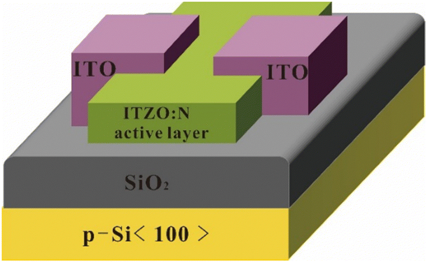 | ||
| Fig. 1 Schematic structure of the ITZO:N TFT. | ||
The thickness of the ITZO:N thin films was measured using a step profiler (Ambios technology company, USA). The structural characteristics were investigated using a X-ray diffractometer (XRD, Rigaku, Japan). The chemical compositions were measured using an energy dispersive spectroscopy system (EDS, Aztec Xmax 50,UK). The surface morphology was observed via a field emission scanning electron microscope (FE-SEM, FEI, NanoSEM 450, USA) and an atomic force microscope (AFM, Oxford Instruments, UK). The optical transmittance was evaluated using a Cary 100 UV/Vis spectrophotometer (Varian Company, USA). The electrical performance of ITZO:N TFTs was characterized using a 4200 semiconductor characterization system (Keithley, USA).
3. Results and discussion
ITZO:N thin films were prepared with RF powers of 50, 60, 70 and 80 W, respectively. The corresponding XRD analysis results are shown in Fig. 2. All the films show an amorphous structure, which is consistent with the glass substrate. No significant diffraction peak can be detected, and the halo peaks in this figure can be attributed to the substrate. It is clear that the amorphous nature of ITZO:N thin films has not changed with the increase in the sputtering power. Zhong et al. reported that the formation of the ITZO amorphous phase is due to the reorganization of the amorphous network between the hexagonal ZnO and ITO.25 Besides, the introduction of nitrogen and the ambient deposition temperature also contribute to lowering the film's crystallinity. A similar phenomenon has also been reported elsewhere.24,26 Since one of the essential factors that affect device performance is stoichiometry, the atomic concentration of ITZO:N films prepared at different RF powers was studied. In general, the contents of In, Sn and Zn elements show minor variations, approximately 35%, 14% and 51%, respectively. However, it can be seen that In+Sn and Zn show opposite trends in Fig. 3. This is probably due to the increase in sputtering power, where indium and tin elements with larger mass are sputtered more from the target. | ||
| Fig. 2 XRD patterns of ITZO:N thin films deposited at different RF powers. | ||
 | ||
| Fig. 3 Atomic concentrations of ITZO:N thin films deposited at different RF powers. | ||
Fig. 4a–d show the surface morphology of ITZO:N thin films fabricated at different RF powers. As can be seen from this figure, ITZO:N films are composed of small spherical particles. When the RF power increases from 50 W to 60 W, the root mean square (RMS) roughness of ITZO:N films decreases from 1.16 to 0.59 nm (see Fig. 4e–f), and the individually distributed grain density on the film's surface also significantly reduces. This is due to the elevated sputtering power providing more energy to the incident particles, which leads to an increase in their migration ability and the local bonding order in the growing film.27,28 Thus, ITZO:N thin films prepared at 60 W are denser and smoother compared to the films deposited at a sputtering power of 50 W. When the RF power further increases to 70 W and 80 W, the incident particles with excessive energy bombard the substrate, resulting in the destruction of the surface structure of ITZO:N thin films. Especially, at a sputtering power of 80 W, the bombardment of the incident particles with high energy will induce lots of defects in the film (noted by red circles in Fig. 4d). This will to some extent degrade the TFT's performance. In addition, with high RF power, more sputtering particles arrive at the substrate and do not have enough time to migrate, leading to roughness on the film's surface.29 This behavior is consistent with the situation of ITZO films reported by Tong et al.30
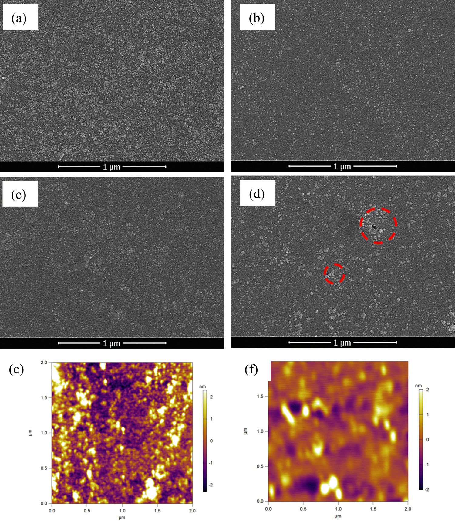 | ||
| Fig. 4 SEM images of ITZO:N thin films deposited at different RF powers: (a) 50 W, (b) 60 W, (c) 70 W, and (d) 80 W. AFM images of (e) 50 W and (f) 60 W. | ||
Fig. 5 shows the optical transmittance curves of ITZO:N thin films prepared with different sputtering powers. The average transmittance in the visible range (380–780 nm) of ITZO:N films always approaches or exceeds 90%. For the films prepared with RF powers of 50, 60, 70 and 80 W, these values are 90.71%, 91.01%, 89.04% and 89.51%. This indicates that the RF power has little effect on the transmittance of the thin films. All ITZO:N thin films possess ideal transmission in the visible region. Besides, the minor variation of the film's transmittance may be related to the incident light scattering caused by the variation of the grain size and the amount of defects in the films.
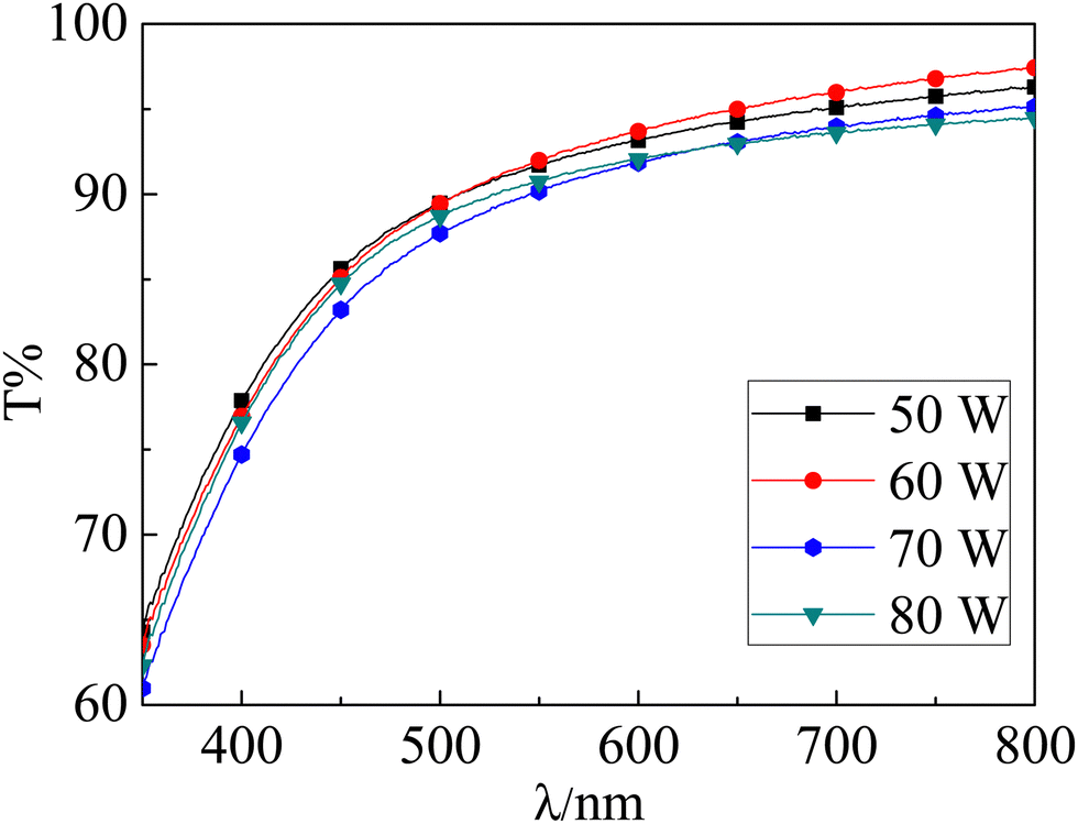 | ||
| Fig. 5 Optical transmittance of ITZO:N thin films deposited at different RF powers. | ||
As a direct band gap semiconductor material, the optical band gaps (Eg) of ITZO:N thin films can be estimated using the Tauc relation (αhν)2 = A(hν − Eg), where α is the absorption coefficient, A is a constant and hv is the photon energy. As shown in Fig. 6, the optical band gaps increase monotonously from 3.44 to 3.54 eV when the RF power increases from 50 W to 80 W. We speculate that such a tendency may relate to the Burstein–Moss effect, i.e., the broadening of optical band gaps is attributed to a higher carrier concentration, which is consistent with the experimental results of the carrier concentration from the transfer characteristics measurement (see Table 1).
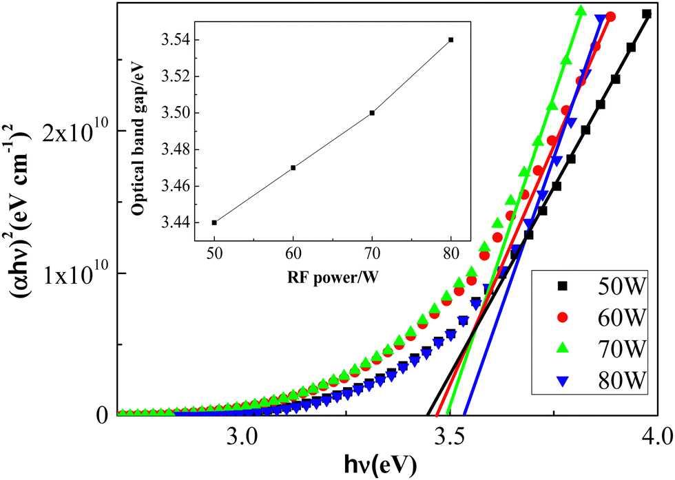 | ||
| Fig. 6 Optical band gaps of ITZO:N thin films deposited at different RF powers. | ||
| RF power W | S (V dec−1) | N s max × 1012 (cm−3) | I on/off | μ FE (cm2 V−1 s−1) | V th (V) | N CH × 1017 (cm−3) |
|---|---|---|---|---|---|---|
| 50 | 2.3 | 2.93 | 104 | 0.13 | 2.91 | 0.71 |
| 60 | 0.7 | 0.83 | 106 | 14.66 | 1.97 | 1.25 |
| 70 | 1.1 | 1.36 | 105 | 1.51 | 0.32 | 1.74 |
| 80 | 1.5 | 1.89 | 105 | 1.06 | 1.16 | 2.36 |
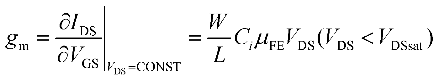
Fig. 7 shows the transfer characteristic curves of ITZO:N TFTs. The VGS is swept from −12 to 25 V while the VDS is fixed at 5 V. The transfer curves of the devices exhibit abnormal properties with hump-shaped features. This behavior indicates the presence of a main channel and a parasitic channel in the device. It is considered that the adsorption of water on the channel, generating a local electric field, may be the main factor in electrical testing under atmospheric conditions.31 It can be seen from the curves that the subthreshold swing (S) of devices decreases first and then increases as the sputtering power increases. S is extracted from the slope of the linear region of the transfer characteristic curves. It is generally considered as an indicator of the power consumption of the devices. The value of S is strongly dependent on the state density (NmaxS) of the active layer/gate dielectric layer interface (eqn (1)):
 | (1) |
 | ||
| Fig. 7 Transfer characteristic curves of ITZO TFTs deposited at different RF powers. | ||
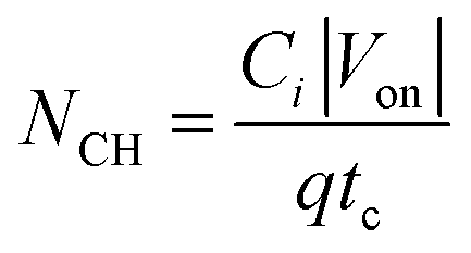
The threshold voltage (Vth), field-effect mobility (μFE) and carrier concentration (NCH) of the TFT can be obtained from eqn (2)–(4) (gm is the transconductance and Von is the turn-on voltage). Their values are listed in Table 1.
 | (2) |
 | (3) |
 | (4) |
When the RF power is increased to 60 W, Sn–O and In–O bonds can be broken by Ar+ ions with higher energy.34 Along with the substitution of In3+ ions by Zn2+/Sn4+ pairs, the defects such as oxygen vacancies and (SnIn)˙ tend to be formed, resulting in generating extra free electrons and improving the carrier concentration.20,37 Then, |Vth| decreases due to the higher number of free electrons.5 Moreover, the film is uniform and compact when the RF power is 60 W, a small amount of defects exists between the interface of the ITZO:N active layer and the SiO2 gate dielectric layer, resulting in fewer carriers being captured here. Therefore, the μFE of this device is significantly better than those of the other three devices.
When the RF power is increased to 70 W and 80 W, the degradation of the device's performance is related to the poor quality of the active layer. The incident particles with excessive energy bombard the substrate, resulting in lots of defects and impurities in the films and the interface of the active layer/gate dielectric layer. These defects could form the trap center or the scattering center, which could result in a reduction in the carrier mobility.38 In addition, due to the presence of parasitic resistance, the concentration of electrons in the channel increases, causing the threshold voltage to shift negatively. When the RF power is 80 W, the high deposition rate leads to an insufficient oxidation reaction in ITZO films. Thus, more oxygen vacancies are created and the carrier concentration raises.33 The abundant electrons can form a highly conductive channel even under a negative gate voltage.5 Thus, the threshold voltage presents a negative value.
The on/off current ratio (Ion/off) of all TFTs is over 104. With the same off current (Ioff), the on current (Ion) increases first and then decreases with an increase in the sputtering power. In Table 1, the largest Ion/off is obtained when the RF power is 60 W. This is attributed to the optimal ITZO:N active layer quality and the lowest NmaxS in this TFT, in which the carriers can be trapped with little possibility. In contrast, when the RF power is 50 W, fewer carriers in the active layer limit the Ion value of the device. And when the RF power is 70 W or 80 W, due to the high defect density in these devices, μFE and Ion reduce, and the device's performance degrades greatly.
4. Conclusions
Amorphous ITZO:N films were prepared with various RF sputtering powers of 50, 60, 70 and 80 W. The microstructures and optical properties of ITZO:N films and the electrical properties of the corresponding ITZO:N TFTs were investigated, subsequently. The results show that the content of both In and Sn elements increases slightly with increasing sputtering power. The RF power has little effect on the active layer's optical transmittance, but strongly affects the optical band gaps of thin films and the interface quality between the active layer and the substrate in TFTs. When the RF power is fixed at 60 W, the ITZO:N active layer with the lowest NmaxS is uniform and compact. The enhanced carrier concentration in this active layer makes the device possess optimal electrical properties. On further increasing the RF power, the quality of the active layer deteriorates. More electrons can be trapped by the defects, resulting in the degradation of the device's properties.Conflicts of interest
There are no conflicts of interest to declare.Acknowledgements
We gratefully acknowledge the National Key R&D Program of China (2022YFB3706600 and 2022YFE0123000) and the National Natural Science Foundation of China (no. 62004117) and also thank the Physical–Chemical Materials Analytical & Testing Center of Shandong University at Weihai for their assistance with characterization.References
- E. Fortunato, A. Pimentel, L. Pereira, A. Goncalves, G. Lavareda, H. Aguas, I. Ferreira, C. N. Carvalho and R. Martins, High field-effect mobility zinc oxide thin film transistors produced at room temperature, J. Non-Cryst. Solids, 2004, 338, 806–809 CrossRef.
- S. U. Jen, H. Sun, H. P. Chiang, S. C. Chen, J. Y. Chen and X. Wang, Optoelectronic Properties and the Electrical Stability of Ga-Doped ZnO Thin Films Prepared via Radio Frequency Sputtering, Materials, 2016, 9, 987 CrossRef PubMed.
- S. W. Cho, M. G. Yun, C. H. Ahn, S. H. Kim and H. K. Cho, Bi-layer Channel Structure-Based Oxide Thin-Film Transistors Consisting of ZnO and Al-Doped ZnO with Different Al Compositions and Stacking Sequences, Electron. Mater. Lett., 2015, 11, 198–205 CrossRef CAS.
- H. Sun, S. U. Jen, S. C. Chen, S. S. Ye and X. Wang, The electrical stability of In-doped ZnO thin films deposited by RF sputtering, J. Phys. D: Appl. Phys., 2017, 50, 045102 CrossRef.
- P. Barquinha, A. Pimentel, A. Marques, L. Pereira, R. Martins and E. Fortunato, Influence of the semiconductor thickness on the electrical properties of transparent TFTs based on indium zinc oxide, J. Non-Cryst. Solids, 2006, 352, 1749–1752 CrossRef CAS.
- R. Martins, P. Barquinha, L. Pereira, I. Ferreira and E. Fortunato, Role of order and disorder in covalent semiconductors and ionic oxides used to produce thin film transistors, Appl. Phys. A: Mater. Sci. Process., 2007, 89, 37–42 CrossRef CAS.
- A. Yildiz, E. Ozturk, A. Atilgan, M. Sbeta, A. Atli and T. Serin, An Understanding of the Band Gap Shrinkage in Sn-Doped ZnO for Dye-Sensitized Solar Cells, J. Electron. Mater., 2017, 46, 6739–6744 CrossRef CAS.
- S. Q. Dai, T. Wang, R. Li, Q. Wang, Y. B. Ma, L. J. Tian, J. B. Su, Y. Wang, D. Z. Zhou, X. Q. Zhang and Y. S. Wang, Preparation and electrical properties of N-doped ZnSnO thin film transistors, J. Alloys Compd., 2018, 745, 256–261 CrossRef CAS.
- Y. B. Ma, L. J. Tian, Q. Wang, R. Li, S. Q. Dai, T. Wang, H. L. Wang, D. Z. Zhou, X. Q. Zhang and Y. S. Wang, Fabrication and electrical characteristics of Li-N co-doped InZnO TFTs prepared by radio frequency magnetron, J. Alloys Compd., 2017, 702, 659–663 CrossRef CAS.
- H. Sun, S.-U. Jen, H.-P. Chiang, S.-C. Chen, M.-H. Lin, J.-Y. Chen and X. Wang, Investigation of optoelectronic performance in In, Ga co-doped ZnO thin films with various In and Ga levels, Thin Solid Films, 2017, 641, 12–18 CrossRef CAS.
- A. Olziersky, P. Barquinha, A. Vila, C. Magana, E. Fortunato, J. R. Morante and R. Martins, Role of Ga2O3-In2O3-ZnO channel composition on the electrical performance of thin-film transistors, Mater. Chem. Phys., 2011, 131, 512–518 CrossRef CAS.
- A. S. Shikoh, G. S. Choi, S. Hong, K. S. Jeong and J. Kim, High-sensitivity hybrid PbSe/ITZO thin film-based phototransistor detecting from 2100 to 2500 nm near-infrared illumination, Nanotechnology, 2022, 33, 165501 CrossRef PubMed.
- D. B. Buchholz, J. Liu, T. J. Marks, M. Zhang and R. P. H. Chang, Control and Characterization of the Structural, Electrical, and Optical Properties of Amorphous Zinc-Indium-Tin Oxide Thin Films, ACS Appl. Mater. Interfaces, 2009, 1, 2147–2153 CrossRef CAS PubMed.
- J. A. Lee, Y. W. Heo, J. H. Lee, H. Y. Lee and J. J. Kim, Structural and Optical Characteristics of Zn-Rich In2O3-SnO2-ZnO (ITZO) Thin Films Prepared by Radio Frequency Magnetron Sputtering, J. Nanoelectron. Optoelectron., 2017, 12, 598–601 CrossRef CAS.
- M. Nakata, C. M. Zhao and J. Kanicki, DC sputtered amorphous In-Sn-Zn-O thin-film transistors: Electrical properties and stability, Solid-State Electron., 2016, 116, 22–29 CrossRef CAS.
- Y. M. Kang, D. Y. Lee, J. R. Lee, P. K. Song, G. H. Lee and J. H. Yoon, Transparent Conductive ITZO Films Deposited by Using a Magnetron Co-Sputtering System Using Two Cathodes, J. Korean Phys. Soc., 2009, 55, 1901–1905 CrossRef CAS.
- J. Y. Noh, H. C. Kim, H. H. Nahm, Y. S. Kim, D. H. Kim, B. D. Ahn, J. H. Lim, G. H. Kim, J. H. Lee and J. H. Song, Cation composition effects on electronic structures of In-Sn-Zn-O amorphous semiconductors, J. Appl. Phys., 2013, 113, 183706 CrossRef.
- J. Robertson, Physics of amorphous conducting oxides, J. Non-Cryst. Solids, 2008, 354, 2791–2795 CrossRef CAS.
- G. D. Robertson and D. J. Oconnor, Magnetic field effects on float-zone Si crystal growth: 2-strong trasvers fields, J. Cryst. Growth, 1986, 76, 100–110 CrossRef CAS.
- Y. B. Lu, T. L. Yang, Z. C. Ling, W. Y. Cong, P. Zhang, Y. H. Li and Y. Q. Xin, How does the multiple constituent affect the carrier generation and charge transport in multicomponent TCOs of In-Zn-Sn oxide, J. Mater. Chem. C, 2015, 3, 7727–7737 RSC.
- J. Raja, K. Jang, N. Hong Hanh, T. Thanh Thuy, W. Choi and J. Yi, Enhancement of electrical stability of a-IGZO TFTs by improving the surface morphology and packing density of active channel, Curr. Appl. Phys., 2013, 13, 246–251 CrossRef.
- P. T. Liu, Y. T. Chou, L. F. Teng, F. H. Li and H. P. Shieh, Nitrogenated amorphous InGaZnO thin film transistor, Appl. Phys. Lett., 2011, 98, 052102 CrossRef.
- C. E. Kim and I. Yun, Effects of nitrogen doping on device characteristics of InSnO thin film transistor, Appl. Phys. Lett., 2012, 100, 013501 CrossRef.
- Z. Y. Li, H. Z. Yang, S. C. Chen, Y. B. Lu, Y. Q. Xin, T. L. Yang and H. Sun, Impact of active layer thickness of nitrogen-doped In-Sn-Zn-O films on materials and thin filmtransistor performances, J. Phys. D: Appl. Phys., 2018, 51, 175101 CrossRef.
- W. Zhong, G. Y. Li, L. F. Lan, B. Li and R. S. Chen, Effects of annealing temperature on properties of InSnZnO thin film transistors prepared by Co-sputtering, RSC Adv., 2018, 8, 34817–34822 RSC.
- J. Junjun, Y. Torigoshi, A. Suko, S. I. Nakamura, E. Kawashima, F. Utsuno and Y. Shigesato, Effect of nitrogen addition on the structural, electrical, and optical properties of In-Sn-Zn oxide thin films, Appl. Surf. Sci., 2017, 396, 897–901 CrossRef.
- R. G. Waykar, A. S. Pawbake, R. R. Kulkarni, A. A. Jadhavar, A. M. Funde, V. S. Waman, H. M. Pathan and S. R. Jadkar, Influence of RF power on structural, morphology, electrical, composition and optical properties of Al-doped ZnO films deposited by RF magnetron sputtering, J. Mater. Sci.: Mater. Electron., 2016, 27, 1134–1143 CrossRef CAS.
- H. Q. Chiang, B. R. McFarlane, D. Hong, R. E. Presley and J. F. Wager, Processing effects on the stability of amorphous indium gallium zinc oxide thin-film transistors, J. Non-Cryst. Solids, 2008, 354, 2826–2830 CrossRef CAS.
- T. C. Lin, W. C. Huang and W. C. Lan, A study on the electrical and optical characteristics of IGZO films, J. Mater. Sci.: Mater. Electron., 2014, 25, 3077–3084 CrossRef CAS.
- Y. Tong, K. L. Wang, Y. Y. Liu, Y. H. Li, S. M. Song and T. L. Yang, Effects of RF power on structure,morphology and photoelectric properties of ITZO thin films, J. Synth. Cryst., 2015, 44, 2338–4249 CAS.
- S. Y. Huang, T. C. Chang, M. C. Chen, S. C. Chen, C. T. Tsai, M. C. Hung, C. H. Tu, C. H. Chen, J. J. Chang and W. L. Liau, Effects of Ambient Atmosphere on Electrical Characteristics of Al2O3 Passivated InGaZnO Thin Film Transistors during Positive-Bias-Temperature-Stress Operation Electrochem, Solid-State Lett., 2011, 14, H177–H179 CrossRef CAS.
- N. Cam Phu Thi, J. Raja, S. Kim, K. Jang, A. H. T. Le, Y.-J. Lee and J. Yi, Enhanced electrical properties of oxide semiconductor thin-film transistors with high conductivity thin layer insertion for the channel region, Appl. Surf. Sci., 2017, 396, 1472–1477 CrossRef.
- Y. Y. Liang, K. S. Jang, S. Velumani, C. P. T. Nguyen and J. S. Yi, Effects of interface trap density on the electrical performance of amorphous InSnZnO thin-film transistor, J. Semicond., 2015, 36, 024007 CrossRef.
- F. C. Liu, Z. n Yu, W. S. Yang, H. C. Zheng and S. Y. Zhang, Gate bias stress induced instability of InGaZnO thin film transistor under different sputter power, Opt. Tech., 2014, 40, 476–480 CrossRef.
- J. F. Shi, C. Y. Dong, W. J. Dai, W. J. Wu, Y. T. Chen and R. Z. Zhang, The influence of RF power on the electrical properties of sputtered amorphous In-Ga-Zn-O thin films and devices, J. Semicond., 2013, 34, 56–60 Search PubMed.
- S. S. Li, C. X. Liang, X. X. Wang, Y. H. Li, S. M. Song, Y. Q. Xin and T. L. Yang, The preparation and characteristics research of high mobility amorphous indium gallium zinc oxide thin-film transistors, Acta Phys. Sin., 2013, 62, 077302 CrossRef.
- N. Q. Wang, Q. Zhang and H. P. Shieh, Influence of Double Channel Layers on the Performance of Nitrogen Doped Indium-zinc-oxide Thin Film Transistors, J. Inorg. Mater., 2016, 31, 745–750 CrossRef CAS.
- B. Du Ahn, K. H. Lee, J. Park and J.-S. Park, The effect of nitrogen incorporation in Ge-In-Ga-O semiconductor and the associated thin film transistors, Appl. Surf. Sci., 2015, 355, 1267–1271 CrossRef.
| This journal is © The Royal Society of Chemistry 2023 |