
 Open Access Article
 This Open Access Article is licensed under a
 Creative Commons Attribution 3.0 Unported Licence
Femtosecond induced third-order optical nonlinearity in quasi 2D Ruddlesden–Popper perovskite film deciphered using Z-scan†
Aamir
Mushtaq
 a,
Bapi
Pradhan
b,
Dushyant
Kushavah
a,
Yiyue
Zhang
b,
Denys
Naumenko
c,
Heinz
Amenitsch
c,
Johan
Hofkens
bd and
Suman Kalyan
Pal
*a
a,
Bapi
Pradhan
b,
Dushyant
Kushavah
a,
Yiyue
Zhang
b,
Denys
Naumenko
c,
Heinz
Amenitsch
c,
Johan
Hofkens
bd and
Suman Kalyan
Pal
*a
aSchool of Basic Sciences and Advanced Material Research Center, Indian Institute of Technology Mandi, Kamand 175005, Himachal Pradesh, India. E-mail: suman@iitmandi.ac.in
bDepartment of Chemistry, KU Leuven, Celestijnenlaan 200F, 3001 Heverlee, Belgium
cInstitute of Inorganic Chemistry, Graz University of Technology, Stremayrgasse 9/V, Graz, 8010, Austria
dMax Planck Institute for Polymer Research, Ackermannweg 10, 55128 Mainz, Germany
First published on 17th August 2022
Abstract
Ruddlesden–Popper perovskite is a class of layered halide perovskite which gained much attention over the past few years in the field of photovoltaics. Herein, we have presented a compendious sketch of third-order nonlinear optical (NLO) properties of (PEA)2Cs4Pb5Br16, a quasi-two-dimensional (2D) perovskite using femtosecond Z-scan technique at 800 nm. Our open aperture (OA) Z-scan measurements unveiled saturable absorption (SA) behaviour of the 2D perovskite with a nonlinear absorption coefficient of −13.83 cm GW−1, which is an order of magnitude higher than other 2D materials. Nonetheless, the self-defocusing effect has been demonstrated using a closed aperture (CA) Z-scan measurement. High nonlinear absorption coefficient and low saturation intensity (38.81 GW cm−2) infer that (PEA)2Cs4Pb5Br16 perovskite film could be useful for ultrafast photonic applications.
Introduction
Nonlinear optics has broad applications in laser technology which includes optical parametric amplification, electro–optic switching, frequency doubling and mixing. The study of nonlinear optical (NLO) properties becomes imperative from the technological point of view to design NLO devices and for the understanding of underlying mechanisms governing light-matter interaction. Ultrashort laser pulses can be generated by exploiting the NLO property, saturable absorption (SA) and hence saturable absorber is the key optical component in pulsed lasers. Semiconductor saturable absorber mirror (SESAM) is commercially used as a saturable absorber because of its high stability, but it has disadvantages of complex fabrication processes and limited bandwidth.1 To develop ultrafast lasers, different NLO materials have been investigated over recent years.2 For example, carbon nanotubes (CNTs) were reported to possess excellent NLO responses. But, this NLO behaviour depends on the distribution of the diameter of CNT.3,4 On the other hand, graphene and graphene analogue two dimensional (2D) materials like transition metal dichalcogenides (TMDCs), transition metal monochalcogenides (TMMCs.), black phosphorous and related materials have shown application potential in ultrafast photonics because of their striking NLO response.5–11Recently, perovskites materials have gained much importance in the field of photonics owing to their NLO properties.12 Li et al. reported an SA response from the CsPbBr3 quantum dots (QDs) with nonlinear absorption coefficient (αNL) −0.35 cm GW−1 and saturation intensity (Isat) 11 GW cm−2.13 In another study, cubic crystals of CsPbBr3 have been shown to exhibit two-photon absorption (TPA) responses with a TPA coefficient of 9.7 × 10⁻² cm GW−1.14 Ruddlesden–Popper perovskite (RPP), are quasi-2D perovskites with the general formula A*2(A)n−1PbnX3n+1, where A* is long-chain aromatic ammonium or alkyl cation, n is the number of octahedral layers in the perovskite-like stack and if n is large (infinity) the resultant structure will be an ordinary 3D perovskite. This class of layered halide perovskite material is on the rise with improved ambient stability.15,16 Cao et al. and Qiu et al. in separate reports demonstrated the role of solvent choice and spin coating conditions in enhancing the stability of 2D perovskite films.17,18 Recently, Liang et al. reported less than 10% efficiency degradation in 2D Ruddlesden–Popper perovskites under continuous light illumination for 1100 hours.19 There might be other approaches under trails that are intelligently engineered to combat stability related issues.
In RPPs, organic ligand layers are bonded via van der Waals forces and as a result they can be exfoliated easily into 2D flakes. RPPs display fantastic optical properties such as large exciton binding energy, bandgap tunability over ultraviolet to visible by changing layer number and strong light-matter coupling.20,21 Benefiting from these properties, RPPs have shown promise for applications in solar cells, LEDs, photodetectors and field-effect transistors.22,23 However, a comprehensive sketch of the third-order nonlinear properties of RPPs is still missing. Herein, we have deciphered the NLO properties of highly optical stable quasi-two-dimensional (PEA)2Cs4Pb5Br16 (Ruddlesden–Popper) perovskite film (PEA= phenylethylammonium) using open and closed aperture Z-scan techniques. The film of an RPP, (PEA)2Cs4Pb5Br16 was prepared by adopting a synthesis method from previous literature.24 The RRP film exhibits NLO behaviour due to single photon absorption resulting in saturable absorption and we also observed self-defocusing behaviour. We compared the results with different reported materials near the IR regime which indicated that the 2D RRP film has superior optical nonlinear behaviour. This research has important research value for furthering the important application of Ruddlesden-Popper perovskites in the field of photonics devices.
Preparation and characterization of the perovskite film
For the preparation of the (PEA)2Cs4Pb5Br16 perovskite film molar stoichiometric ratios of all the components were dissolved in 1 ml DMSO (0.5 mmol PbBr2, 0.37 mmol CsBr and 0.25 mmol PEABr) followed by spin coating on a coverslip at 1200 rpm for 10 s. Chlorobenzene was dropped as an antisolvent before 30s of the final spin–coating process followed by annealing the film at 90 °C for 10 min. The thin films were stored in the glove box under an inert atmosphere. The film crystalline structure has been characterized by grazing-incidence wide-angle X-ray scattering (GIWAXS) measurements. 2D GIWAXS patterns (Fig. 1a and b) have been acquired at the surface- and depth-sensitive conditions, i.e. at incident angles of 0.22 and 1.3 degrees with corresponding X-ray penetration depths of 3.7 nm and 234.9 nm into the (PEA)2Cs4Pb5Br16 film.25 The former is characterized by prominent diffraction spots (Fig. 1a) indicating the presence of a few-layer perovskite structure at the surface. The appearance of the diffuse rings in the latter (Fig. 1b) suggests that the orientation of the layered structure becomes more random inside the film. To reveal the crystal orientation relative to the substrate three-dimensional structure indexing has been performed using an orthorhombic CsPbBr3 phase26 and overlaid with 2D GIWAXS patterns.27 It has been found that a mixture of two orientations in the film gives rise to the most prominent diffraction spots. One orientation is characterized by the crystal b-axis perpendicular to the substrate plane, i.e. (010) is the out-of-plane direction, and another one is with (101) orientation in the out-of-plane direction as depicted in Fig. 1d. The latter orientation is more preferable and constitutes 58.8% of all crystalline grains (Fig. S1, ESI†). The average grain size has been estimated at 28.4 ± 3.3 nm using the Scherrer formula which accounts for the resolution of the apparatus.28 Three diffraction rings originating from PEA layers have also been identified (Fig. 1b and c). Their intensity distribution with pronounced maxima in the out-of-plane direction and d-spacing of 1.67 nm (Fig. 1b) suggests that PEA multilayers are preferentially oriented parallel to the substrate. Additionally, it suggests that 1.67 nm is the distance between the layered perovskites.29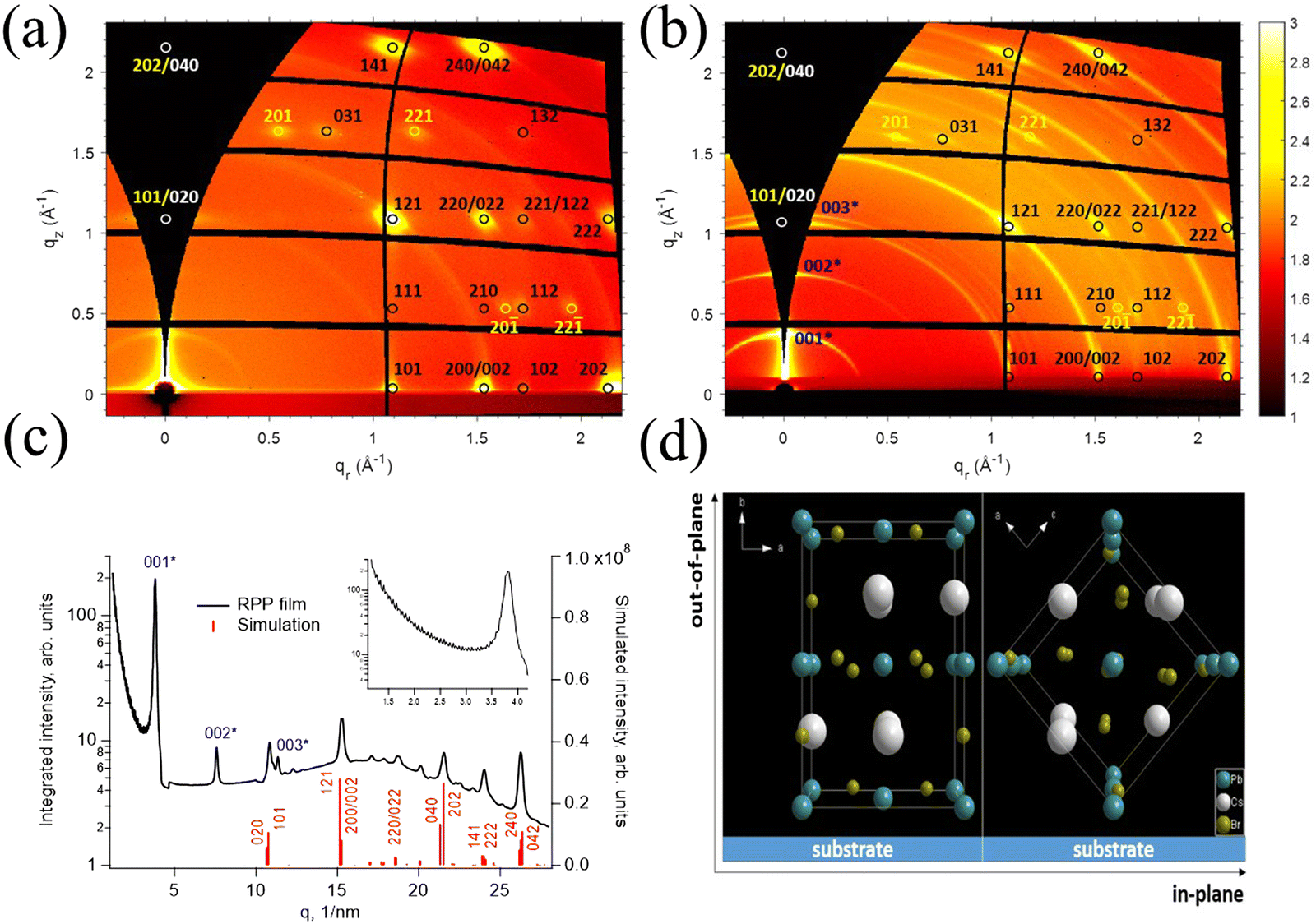 | ||
| Fig. 1 2D GIWAXS patterns of the (PEA)2Cs4Pb5Br16 (RPP) film acquired at an incident angle of 0.22° (a) and 1.3° (b). (c) Azimuthal integration of the GIWAXS pattern depicted in panel (b) (black curve) and simulated powder diffraction (red sticks). (d) Two crystal orientations have been used to index the most prominent reflections in 2D GIWAXS patterns shown in (a and, b). The left orientation is represented by black and white markers, while yellow markers are used for the right orientation. The peaks highlighted in blue colour in (b and c) originate from PEA layers. The CsPbBr3 crystal data are taken from ref. 22.26 | ||
Fig. 2a represents the SEM image of quasi 2D perovskite film measured using NanoSem 450 (FE-SEM) to analyse the submicrometre-scale structural morphology. The inset of Fig. 2a is a high-resolution SEM image, which confirms 2D type faceted platelets with roughly rectangular shapes with sizes between 50 nm and 300 nm. Fig. 2b shows the absorption spectrum of the perovskite film, recorded using a Lamda 950 UV-Vis spectrophotometer depicting a sharp optical absorption peak around 510 nm. Photoluminescence (PL) was measured on Edinburgh FLS980 using a He–Cd laser (380 nm) at room temperature (Fig. S2, (ESI†)). The PL spectrum is broad with a maximum at 513 nm. The observed broad PL emission could be due to the presence of trap states formed during synthesis.24,30 Both the absorption and PL maxima are consistent with the earlier reports.24 Moreover, time resolved PL measurement provided some clue about the existence of intermediate states in our sample. It can be seen that the PL intensity in Fig. 2c decays quickly at the initial time and then the decay becomes slower. We fitted the decay curve using a biexponential function which reveals short (400 ps, 80%) and longer time components (1.7 ns, 20%) with an average PL lifetime of ∼690 ps. The initial fast decay component could be assigned to the recombination process via trap/defect states and the long component could be ascribed to the band to band radiative recombination of carriers.24,31,32
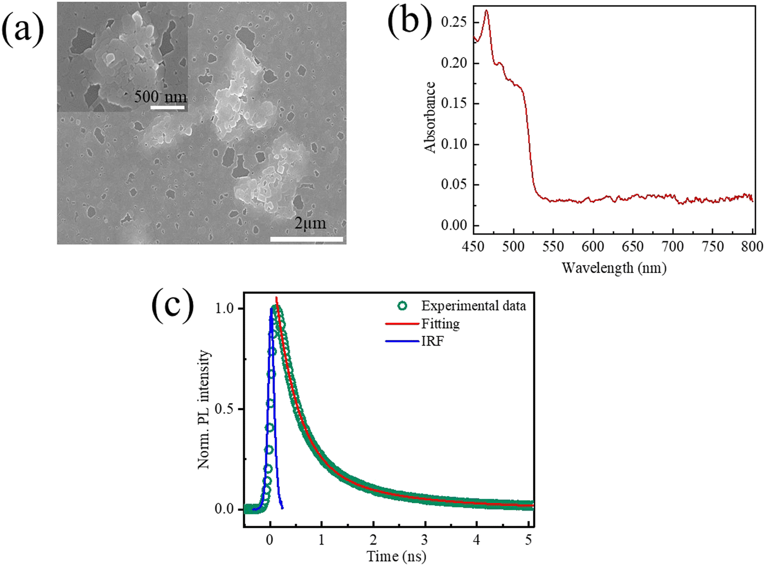 | ||
| Fig. 2 (a) SEM images of perovskite film (Inset: high-resolution SEM image). (b) Absorption and (c) PL decay kinetics of the perovskite film recorded using TCSPC. | ||
A spin coated film of the perovskite on a coverslip was used to carry out the NLO study. To scrutinize the ultrafast nonlinear response, we carried out conventional open aperture (OA) and closed aperture (CA) Z-scan measurements in the near IR wavelength region (800 nm). The Z-scan setup used in this study has already been described in our previous work.33,34 The output from a Ti:sapphire regenerative amplifier (Spitfire ace, Spectra Physics) seeded by an oscillator (Mai Tai SP, Spectra Physics) was used as the excitation source. After bouncing from a couple of mirrors laser was finally focused on a sample mounted over a computer-controlled transitional stage with the help of a convex lens of focal length 10 cm. The transmittance of the sample as a function of sample position is recorded with the help of photodetectors from the Pascher instrument. The beam waist at the focus was measured to be 33.05 μm. The pulse width of the laser light operated at 1 kHz repetition rate (RR) at the sample position was 57 fs. The Z-scan setup used to carry out nonlinear optical measurement is shown in Fig. 3.
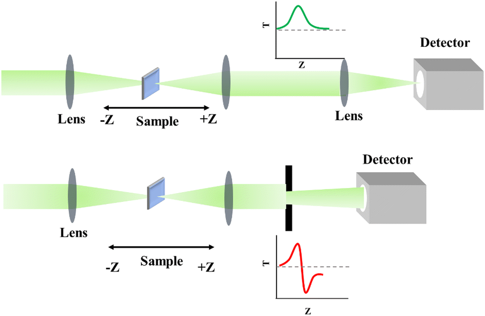 | ||
| Fig. 3 Schematic representation of the Z-scan setup used for the NLO study. | ||
Z-Scan experiment and discussion
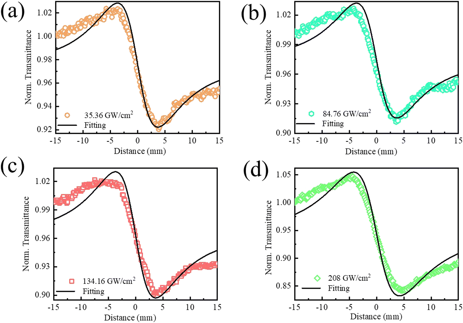
Fig. 4 shows the plots of normalised transmittance (for OA Z-scan) as a function of sample position. Clearly, as the samples approach toward the focus, the normalized transmittance of the sample increases, which could be ascribed to the SA process. The decrease in absorption of the sample due to SA results in the increased intensity of transmitted light. Nonetheless, as the input fluence increases the strength of the peak transmission signal increases and becomes maximum at a higher fluence. Since the bandgap of the RPP is 2.4 eV, an incident photon (1.55 eV) does not have enough energy to lift an electron from the valence to the conduction band. However, excitation photons can cause transitions of electrons (from valence band) into intermediate states. Thus, the observed SA behaviour could be attributed to the filling of defect or intermediate states.35 However, these trap states act like a bridge for electrons to jump into the conduction band from the valence band by absorbing multi-photons with lower energy thus making the photo-bleaching effect possible. As excitation intensity increases the excitation and re-excitation of electrons from the valence band to a higher energy level (conduction band/trap states) became very fast while the reverse relaxation process slows down. When the excitation rate is faster than the relaxation rate the net electrons population increases in the excited state inducing reduction of photon absorption (SA effect). When excitation intensity is strong enough, at that condition due to Pauli blocking principle all available states at a higher energy level get occupied and are unable to accommodate extra photo-generated carriers resulting in a photo-bleaching effect.36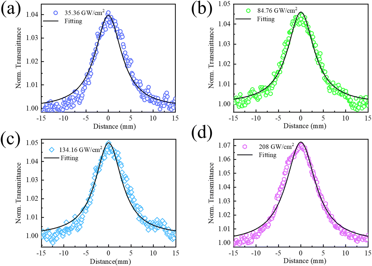 | ||
| Fig. 4 Open aperture (OA) Z-scan curves obtained at an excitation wavelength of 800 nm for (a) 35.36, (b) 84.76, (c) 134.16 and (d) 208 GW cm−2 input intensities. The solid line in each figure represents the fitting of experimental data. | ||
The steady state and time-resolved PL suggested the existence of defect/trap states, which form optically active intermediate states below the bandgap in the (PEA)2Cs4Pb5Br16 perovskite.
It is worth noting that no SA response was observed from the coverslip under the same excitation (Fig. S3a, ESI†). We measured the absorption spectrum of the irradiated area of the perovskite film after Z-scan measurements to verify the sample decomposition. Almost identical absorption behaviour of the perovskite film after measurements (Fig. S3b, ESI†) suggests that the possibility of sample degradation under intense laser light is very slim. Furthermore, as we have employed ultrashort pulses at 1 kHz nonlinear scattering and thermal effects are expected to be much weaker.37,38 It is worth mentioning that for laser pulses operated at an MHz repetition rate thermal contribution plays a significant role in nonlinear parameters.39
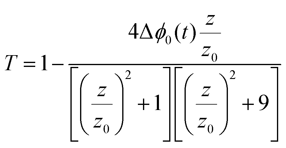
To quantitatively estimate the NLO coefficient of the (PEA)2Cs4Pb5Br16 perovskite film, we switched to fitted Z-scan curves using the following nonlinear propagation equation.
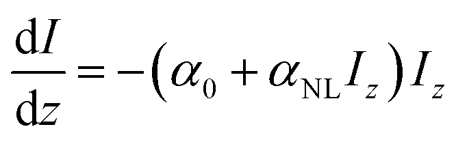 | (1) |
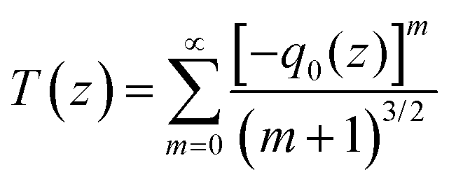 | (2) |
 , m is an integer and equal to 1 in the present case.
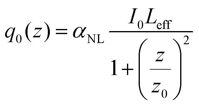
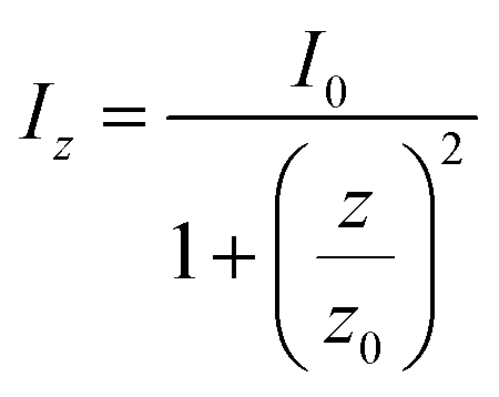
 is the effective path length, I0 is the on-axis peak intensity at the focus and z0 is the Rayleigh range. The given path length, L was measured from the cross-sectional SEM image (Fig. S4, ESI†) and found to be around 2.422 μm. It is clear from Fig. 4 that the experimental data is fitted well with eqn 2. The extracted values of nonlinear absorption coefficients (αNL) from fitting are tabulated in Table 1. The values of αNL at 800 nm are as high as −13.83 × 10⁻⁹ cm W−1. Furthermore, to extract the value of saturation intensity, we plotted transmittance as a function of intensity (Fig. 5a) and used the following equation to fit the curve.10
 | (3) |
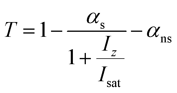
 , αs is the modulation depth, αns is the nonsaturable component, and Isat is the saturation intensity. Fitting results (using eqn 3) reveal that perovskite film exhibits a saturation intensity of 38.81 GW cm−2 and a modulation depth of 8%. The scheme of the SA process involved is shown in Fig. 5b.
| S. no | I 0 (GW cm−2) | α NL × 10−9 (cm W−1) | n 2 × 10⁻¹¹ (cm2 W) |
|---|---|---|---|
| 1 | 35.36 | −13.8 | 4.1 |
| 2 | 84.76 | −6.7 | 1.8 |
| 3 | 134.16 | −4.6 | 1.3 |
| 4 | 208 | −4.3 | 1.4 |
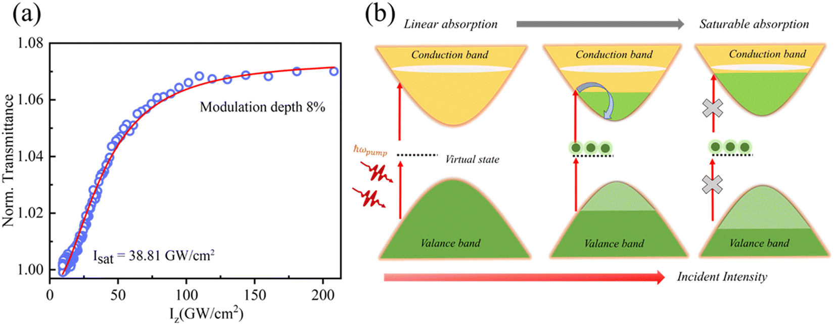 | ||
| Fig. 5 (a) Normalised transmission as a function of intensity for 208 GW cm−2. (b) Schematic sketch of the mechanism behind SA in the sample. | ||
We have made a comparison of NLO properties of our quasi 2D perovskite film with other contemporary materials. Nonetheless, both blue and green emissive CsPbBr3 quantum dots possess nonlinear absorption coefficients (αNL) of −1.7 and −0.68 cm GW−1, respectively at 800 nm.40 Rao et al. reported a saturation intensity (Isat) of 500 and 95 GW cm−2 for CsPbBr3 cubic nanocrystals and nanorods, respectively under 600 nm laser excitation.41 The value of αNL (−116 to −69 × 103 cm GW−1) is reported to be very high for the 2D sheet of a RRP, (BA)2PbI4. This extremely large value of αNL was attributed to a pondermotive and relativistic nonlinear effect triggered by plasma formation.42 SA behaviour has been demonstrated in Cs2NaBiI6 and Cs2KBiI6 inorganic double perovskite films with αNL of −6.23 × 10⁻³ and −1.14 × 10⁻³ cm GW−1, respectively using a 1030 nm laser light of pulse width 370 fs.43 Likewise, the MAPbI3 film was carefully inspected by Kalanoor et al. under laser pulses of different repetition rates, pulse widths and wavelengths. According to them, the large value of αNL of MAPbI3 at 1028 nm could arise due to substantial contribution from free carrier absorption.44 Furthermore, we compare the NLO properties of our 2D perovskite with other 2D materials.
It is clear from the comparison that the value of the nonlinear absorption coefficient for the (PEA)2Cs4Pb5Br16 perovskite film is comparable to other perovskites, but two to three orders of magnitude larger than 2D transition metal dichalcogenides (TMDCs), transition metal monochalcogenides (MMCs), black phosphorous and few layer MXenes. The saturation intensity of (PEA)2Cs4Pb5Br16 is found to be much lower as compared to other 2D materials and comparable/lower than other perovskites (Table 2). It is important to mention that the input intensity employed in previous studies is of the order GW cm−2.13,50,51 Passive Q-switched laser operation had been demonstrated using perovskites (0D, 2D), TMDCs, and MXenes showing a saturable absorption response at input intensities of the order of GW cm−2.13,50,52,53 We speculate, based on previous studies, that pulsed laser operation could be possible using our (PEA)2Cs4Pb5Br16 perovskite based saturable absorber, which further requires realistic experimental validation.
| Materials | Excitation | α NL × 10−9 (cm W−1) | n 2 × 10⁻¹¹ (cm2 W) | I s (GW cm−2) | Ref. |
|---|---|---|---|---|---|
| SnS sheets | 800 nm, 100 fs, 1kHz | −4.65 × 10⁻³ | — | 158 | 45 |
| Graphene | 800 nm. 100 fs | −8.28 × 10⁻³ | — | 764 | 46 |
| Black phosphorus | 800 nm. 100 fs | −1.38 × 10⁻² | — | 459 | 46 |
| MoS2 sheets | 800 nm, 100 fs, 1kHz | −2.42 × 10⁻² | — | 381 | 47 |
| MoTe2 sheets | 800 nm, 100 fs, 1kHz | −3.7 × 10⁻³ | — | 217 | 47 |
| MoSe2 sheets | 800 nm, 100 fs, 1kHz | −2.54 × 10⁻³ | — |
|
47 |
| Au-CsPbBr3 cubic nanocrystals | 800 nm, 130 fs, 76 MHz | −9.93 × 10⁻² to 2.34 × 10⁻¹ | — | — | 48 |
| Few layer MXenes Ti3C2Tx (T = F, O, or OH) | 800 nm, 95 fs, 1kHz | −11.7 × 10⁻³ | −4.66 × 10⁻⁵ | 88.6 | 49 |
| (PEA)2Cs4Pb5Br16, quasi 2D perovskite film | 800 nm, 57 fs, 1kHz | −4.3 | −1.4 | 38.81 | Present work |
Next, we move on to closed aperture (CA) measurements under different excitation intensities. Each curve possesses a “peak-valley” type structure which arises due to self-defocusing, a third-order nonlinear optical process (Fig. 6). The occurrence of a peak (prefocal transmittance maximum) followed by a valley (postfocal transmittance minimum) suggests that the perovskite has a negative nonlinear refractive index (n2 < 0). CA curves were obtained after division with OA data to eliminate the contribution of nonlinear absorption and fitted using the following equation54
 | (4) |
 and λ is the excitation wavelength. The magnitude of the calculated values of nonlinear refractive index using eqn 4 is shown in Table 1. Next, we made a comparison of the nonlinear refractive (n2) index with other perovskites. 2D flakes of layered RRP, (BA)2(MA)Pb2I7 and (BA)2(MA)3Pb4I13 exhibited a nonlinear refractive index of −4.7 × 10⁻¹² and −2 × 10⁻¹² cm2 W−1, respectively.55 Li et al. reported a nonlinear refractive index of −0.14 × 10⁻¹² cm2 W−1 for CsPb(Cl0.53Br0.47)3 cubic crystals.56 Furthermore, self-defocusing was reported in CsPbBr3 nanocrystals (n2 ∼ 10−13 cm−2 W−1 at 600–800 nm) under femtosecond pulse excitations.41 A laser pulse (216 ps) was generated via mode-locking with CsPbBr3 nanocrystals.57 Wei et al. showed the potential of CH3NH3PbBr3 perovskite crystals in modulating spectral and temporal laser profiles, optical limiting and optical stabilization.58 In inorganic double perovskite, Cs2NaBiI6 and Cs2KBiI6 films self-defocusing led to a negative nonlinear refractive index of −1.06 × 10⁻¹⁴ and −1.34 × 10⁻¹⁴ cm2 W−1, respectively.43 A negative nonlinear refractive index (−0.24 × 10⁻¹² cm2 W−1) was observed in a MAPbI3 film under excitation by a femtosecond laser (514 nm) pulse due to self-defocusing behaviour.44 We can infer from the above discussion that our 2D perovskite which has same or even higher values of n2 as compared to other perovskites could be useful in mode locking/Q-switching as well as in pulse shaping.
 | ||
| Fig. 6 Closed aperture (CA) Z-scan curves captured at an excitation wavelength of 800 nm for (a) 35.36, (b) 84.76, (c) 134.16 and (d) 208 GW cm−2 input intensities. | ||
It is important to mention that we used the same parameters in fitting both OA and CA Z-scan curves. CA curves show little asymmetry which could be due to distortion of the Gaussian profile of the laser beam caused by thickness inhomogeneity in the film.59 Estimated error in the measurement is expected to be 10–15% which may arise in measuring peak intensities, fluctuation in laser output and fitting.
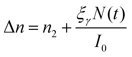
It has been found that increasing the input fluences results in a decrement of n2 which eventually saturates at higher intensities (Fig. 7). This decrease in the nonlinear refractive index can be understood from the following equation.
 | (5) |
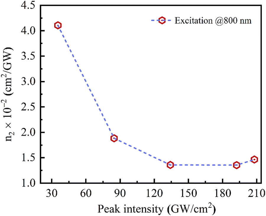 | ||
| Fig. 7 Variation of the nonlinear refractive index as a function of peak intensity. | ||
Here Δn is the effective nonlinear refractive index, N(t) is the carrier density, ξγ is the change in refractive index per unit density of conduction band electrons and I0 is the on-axis peak intensity. As inferred from the above equation, the decrease in refractive index is due to its dependence on light intensity and charge carrier density which tends to saturate at higher intensities.
Conclusion
In conclusion, we investigated third-order nonlinear optical (NLO) properties of the (PEA)2Cs4Pb5Br16 perovskite film using an open and closed aperture femtosecond Z-scan technique. Our OA Z-scan study uncovers the saturable absorption behaviour in the (PEA)2Cs4Pb5Br16 perovskite film which exhibits a low saturation intensity, high nonlinear absorption coefficient, low nonsaturable loss and has the ability to withstand very high input intensity. Moreover, the CA Z-scan reveals a negative nonlinear refractive index because of the self-defocusing effect in our 2D perovskite. Our pioneering research based on 2D RPPs has great implication in strengthening the area of nonlinear research and applications. This demonstration of intriguing NLO properties of the (PEA)2Cs4Pb5Br16 perovskite is expected to accelerate the development of the Ruddlesden–Popper perovskite based on ultrafast photonic devices.Conflicts of interest
There are no conflicts to declare.Acknowledgements
A. M. is thankful to IIT Mandi for his fellowship and Advanced Materials Research Centre for the experimental facilities; B. P. acknowledges a postdoctoral fellowship from the Research Foundation-Flanders (FWO Grant no. 1275521N); Y. Z. acknowledge support from the China Scholarship Council (No. 201908440479); J. H. acknowledges financial support from the Research Foundation–Flanders (Fonds Wetenschappelijk Onderzoek, FWO, Grant No. G0A5817N, G098319N, W002221N, S002019N, and ZW15_09-G0H6316N), the Vlaamse regering through long-term structural funding Methusalem (CASAS2, Meth/15/04), the Onderzoeksraad, KU Leuven Research Fund (iBOF-21-085 PERSIST), and the Max-Planck-Gesellschaft as MPI fellow. The authors also acknowledge the CERIC-ERIC consortium for the fast-track access to the Austrian SAXS beamline at Elettra Sincrotrone Trieste.References
- U. Keller, Nature, 2003, 424, 831–838 CrossRef CAS PubMed.
- A. Martinez and Z. Sun, Nat. Photonics, 2013, 7, 842–845 CrossRef CAS.
- T. Hasan, Z. Sun, F. Wang, F. Bonaccorso, P. H. Tan, A. G. Rozhin and A. C. Ferrari, Adv. Mater., 2009, 21, 3874–3899 CrossRef CAS.
- A. G. Rozhin, Y. Sakakibara, S. Namiki, M. Tokumoto, H. Kataura and Y. Achiba, Appl. Phys. Lett., 2006, 88, 051118 CrossRef.
- Y.-W. Song, S.-Y. Jang, W.-S. Han and M.-K. Bae, Appl. Phys. Lett., 2010, 96, 051122 CrossRef.
- J. Sotor, I. Pasternak, A. Krajewska, W. Strupinski and G. Sobon, Opt. Express, 2015, 23, 27503–27508 CrossRef CAS PubMed.
- H. Zhang, S. B. Lu, J. Zheng, J. Du, S. C. Wen, D. Y. Tang and K. P. Loh, Opt. Express, 2014, 22, 7249–7260 CrossRef CAS PubMed.
- R. I. Woodward, R. C. T. Howe, T. H. Runcorn, G. Hu, F. Torrisi, E. J. R. Kelleher and T. Hasan, Opt. Express, 2015, 23, 20051–20061 CrossRef CAS PubMed.
- F. Xia, H. Wang and Y. Jia, Nat. Commun., 2014, 5, 4458 CrossRef CAS PubMed.
- A. S. Sarkar, A. Mushtaq, D. Kushavah and S. K. Pal, npj 2D Mater. Appl., 2020, 4, 1 CrossRef CAS.
- M. Zhang, J. Li, H. Chen, J. Zhang, J. Yin, T. He, J. Wang, M. Zhang, B. Zhang, J. Yuan, P. Yan and S. Ruan, APL Photonics, 2019, 4, 090801 CrossRef.
- Y. Zhou, Y. Huang, X. Xu, Z. Fan, J. B. Khurgin and Q. Xiong, Appl. Phys. Rev., 2020, 7, 041313 CAS.
- J. Li, H. Dong, B. Xu, S. Zhang, Z. Cai, J. Wang and L. Zhang, Photonics Res., 2017, 5, 457–460 CrossRef CAS.
- Y. Wang, X. Li, X. Zhao, L. Xiao, H. Zeng and H. Sun, Nano Lett., 2016, 16, 448–453 CrossRef CAS PubMed.
- D. H. Cao, C. C. Stoumpos, O. K. Farha, J. T. Hupp and M. G. Kanatzidis, J. Am. Chem. Soc., 2015, 137, 7843–7850 CrossRef CAS PubMed.
- Y. Zhang, M. Keshavarz, E. Debroye, E. Fron, M. C. R. González, D. Naumenko, H. Amenitsch, J. Van de Vondel, S. De Feyter and P. Heremans, Nanophotonics, 2021, 10, 2145–2156 CrossRef CAS.
- D. H. Cao, C. C. Stoumpos, T. Yokoyama, J. L. Logsdon, T.-B. Song, O. K. Farha, M. R. Wasielewski, J. T. Hupp and M. G. Kanatzidis, ACS Energy Lett., 2017, 2, 982–990 CrossRef CAS.
- J. Qiu, Y. Zheng, Y. Xia, L. Chao, Y. Chen and W. Huang, Adv. Funct. Mater., 2019, 29, 1806831 CrossRef CAS.
- C. Liang, H. Gu, Y. Xia, Z. Wang, X. Liu, J. Xia, S. Zuo, Y. Hu, X. Gao, W. Hui, L. Chao, T. Niu, M. Fang, H. Lu, H. Dong, H. Yu, S. Chen, X. Ran, L. Song, B. Li, J. Zhang, Y. Peng, G. Shao, J. Wang, Y. Chen, G. Xing and W. Huang, Nat. Energy, 2021, 6, 38–45 CrossRef CAS.
- Z. Chen, Y. Guo, E. Wertz and J. Shi, Adv. Mater., 2019, 31, 1803514 CrossRef PubMed.
- J. Wang, R. Su, J. Xing, D. Bao, C. Diederichs, S. Liu, T. C. H. Liew, Z. Chen and Q. Xiong, ACS Nano, 2018, 12, 8382–8389 CrossRef CAS PubMed.
- H. Tsai, W. Nie, J.-C. Blancon, C. C. Stoumpos, R. Asadpour, B. Harutyunyan, A. J. Neukirch, R. Verduzco, J. J. Crochet, S. Tretiak, L. Pedesseau, J. Even, M. A. Alam, G. Gupta, J. Lou, P. M. Ajayan, M. J. Bedzyk, M. G. Kanatzidis and A. D. Mohite, Nature, 2016, 536, 312–316 CrossRef CAS PubMed.
- S. Wei, F. Wang, X. Zou, L. Wang, C. Liu, X. Liu, W. Hu, Z. Fan, J. C. Ho and L. Liao, Adv. Mater., 2020, 32, 1907527 CrossRef CAS PubMed.
- Z. Yang, M. Wei, O. Voznyy, P. Todorovic, M. Liu, R. Quintero-Bermudez, P. Chen, J. Z. Fan, A. H. Proppe, L. N. Quan, G. Walters, H. Tan, J.-W. Chang, U. S. Jeng, S. O. Kelley and E. H. Sargent, J. Am. Chem. Soc., 2019, 141, 8296–8305 CrossRef CAS PubMed.
- B. L. Henke, E. M. Gullikson and J. C. Davis, At. Data Nucl. Data Tables, 1993, 54, 181–342 CrossRef CAS.
- C. C. Stoumpos, C. D. Malliakas, J. A. Peters, Z. Liu, M. Sebastian, J. Im, T. C. Chasapis, A. C. Wibowo, D. Y. Chung, A. J. Freeman, B. W. Wessels and M. G. Kanatzidis, Cryst. Growth Des., 2013, 13, 2722–2727 CrossRef CAS.
- Z. Jiang, J. Appl. Crystallogr., 2015, 48, 917–926 CrossRef CAS.
- D.-M. Smilgies, J. Appl. Crystallogr., 2009, 42, 1030–1034 CrossRef CAS PubMed.
- Y. Shang, Y. Liao, Q. Wei, Z. Wang, B. Xiang, Y. Ke, W. Liu and Z. Ning, Sci. Adv., 2019, 5, eaaw8072 CrossRef CAS PubMed.
- D. Y. Park, S.-J. An, C. Lee, D. A. Nguyen, K.-N. Lee and M. S. Jeong, J. Phys. Chem. Lett., 2019, 10, 7942–7948 CrossRef CAS PubMed.
- H.-H. Fang, J. Yang, S. Adjokatse, E. Tekelenburg, M. E. Kamminga, H. Duim, J. Ye, G. R. Blake, J. Even and M. A. Loi, Adv. Funct. Mater., 2020, 30, 1907979 CrossRef CAS.
- B. Yang, X. Mao, F. Hong, W. Meng, Y. Tang, X. Xia, S. Yang, W. Deng and K. Han, J. Am. Chem. Soc., 2018, 140, 17001–17006 CrossRef CAS PubMed.
- A. Mushtaq, D. Kushavah, S. Ghosh and S. K. Pal, Appl. Phys. Lett., 2019, 114, 051902 CrossRef.
- A. Mushtaq, B. Pradhan, D. Kushavah, Y. Zhang, M. Wolf, N. Schrenker, E. Fron, S. Bals, J. Hofkens, E. Debroye and S. K. Pal, ACS Photonics, 2021, 8, 3365–3374 CrossRef CAS.
- X. Zheng, Y. Zhang, R. Chen, X. A. Cheng, Z. Xu and T. Jiang, Opt. Express, 2015, 23, 15616–15623 CrossRef CAS PubMed.
- R.-F. Zhang, D.-Z. Guo and G.-M. Zhang, Appl. Surf. Sci., 2017, 426, 763–769 CrossRef CAS.
- X.-F. Jiang, L. Polavarapu, S. T. Neo, T. Venkatesan and Q.-H. Xu, J. Phys. Chem. Lett., 2012, 3, 785–790 CrossRef CAS PubMed.
- B. Anand, R. Podila, P. Ayala, L. Oliveira, R. Philip, S. S. Sankara Sai, A. A. Zakhidov and A. M. Rao, Nanoscale, 2013, 5, 7271–7276 RSC.
- Y. Wang, X. Yang, T. C. He, Y. Gao, H. V. Demir, X. W. Sun and H. D. Sun, Appl. Phys. Lett., 2013, 102, 021917 CrossRef.
- W.-G. Lu, C. Chen, D. Han, L. Yao, J. Han, H. Zhong and Y. Wang, Adv. Opt. Mater., 2016, 4, 1732–1737 CrossRef CAS.
- K. N. Krishnakanth, S. Seth, A. Samanta and S. V. Rao, Opt. Lett., 2018, 43, 603–606 CrossRef CAS PubMed.
- I. Abdelwahab, P. Dichtl, G. Grinblat, K. Leng, X. Chi, I.-H. Park, M. P. Nielsen, R. F. Oulton, K. P. Loh and S. A. Maier, Adv. Mater., 2019, 31, 1902685 CrossRef PubMed.
- A. Singh, P. Dey, A. Kumari, M. K. Sikdar, P. K. Sahoo, R. Das and T. Maiti, Phys. Chem. Chem. Phys., 2022, 24, 4065–4076 RSC.
- B. S. Kalanoor, L. Gouda, R. Gottesman, S. Tirosh, E. Haltzi, A. Zaban and Y. R. Tischler, ACS Photonics, 2016, 3, 361–370 CrossRef CAS.
- F. Zhang, N. Xu, J. Zhao, Y. Wang, X. Jiang, Y. Zhang, W. Huang, L. Hu, Y. Tang, S. Xu and H. Zhang, Nanophotonics, 2020, 9, 1963–1972 CrossRef CAS.
- K. Wang, B. M. Szydłowska, G. Wang, X. Zhang, J. J. Wang, J. J. Magan, L. Zhang, J. N. Coleman, J. Wang and W. J. Blau, ACS Nano, 2016, 10, 6923–6932 CrossRef CAS PubMed.
- K. Wang, Y. Feng, C. Chang, J. Zhan, C. Wang, Q. Zhao, J. N. Coleman, L. Zhang, W. J. Blau and J. Wang, Nanoscale, 2014, 6, 10530–10535 RSC.
- X. Yan, Y. Shen, H. Liu and X. Yang, J. Mater. Sci., 2020, 55, 10678–10688 CrossRef CAS.
- X. Jiang, S. Liu, W. Liang, S. Luo, Z. He, Y. Ge, H. Wang, R. Cao, F. Zhang, Q. Wen, J. Li, Q. Bao, D. Fan and H. Zhang, Laser Photonics Rev., 2018, 12, 1700229 CrossRef.
- R. Wei, H. Zhang, X. Tian, T. Qiao, Z. Hu, Z. Chen, X. He, Y. Yu and J. Qiu, Nanoscale, 2016, 8, 7704–7710 RSC.
- S. Zhang, X. Zhang, H. Wang, B. Chen, K. Wu, K. Wang, D. Hanlon, J. N. Coleman, J. Chen, L. Zhang and J. Wang, Opt. Mater. Express, 2016, 6, 3159–3168 CrossRef CAS.
- S. Hong, F. Lédée, J. Park, S. Song, H. Lee, Y. S. Lee, B. Kim, D.-I. Yeom, E. Deleporte and K. Oh, Laser Photonics Rev., 2018, 12, 1800118 CrossRef.
- X. Jiang, A. V. Kuklin, A. Baev, Y. Ge, H. Ågren, H. Zhang and P. N. Prasad, Phys. Rep., 2020, 848, 1–58 CrossRef CAS.
- M. Sheik-bahae, A. A. Said and E. W. Van Stryland, Opt. Lett., 1989, 14, 955–957 CrossRef CAS PubMed.
- G. Grinblat, I. Abdelwahab, M. P. Nielsen, P. Dichtl, K. Leng, R. F. Oulton, K. P. Loh and S. A. Maier, ACS Nano, 2019, 13, 9504–9510 CrossRef CAS PubMed.
- J. Li, C. Ren, X. Qiu, X. Lin, R. Chen, C. Yin and T. He, Photonics Res., 2018, 6, 554–559 CrossRef CAS.
- Y. Zhou, Z. Hu, Y. Li, J. Xu, X. Tang and Y. Tang, Appl. Phys. Lett., 2016, 108, 261108 CrossRef.
- T.-C. Wei, S. Mokkapati, T.-Y. Li, C.-H. Lin, G.-R. Lin, C. Jagadish and J.-H. He, Adv. Opt. Mater., 2018, 28, 1707175 Search PubMed.
- K. Kinastowska, K. Piela, M. Gordel, A. Żak, R. Kołkowski and M. Samoć, Phys. Chem. Chem. Phys., 2018, 20, 18862–18872 RSC.
Footnote |
| † Electronic supplementary information (ESI) available: See supplementary material for the synthesis of 2D perovskite film, comparison to other contemporary materials, solvent response and SEM. See DOI: https://doi.org/10.1039/d2ma00724j |
| This journal is © The Royal Society of Chemistry 2022 |