
 Open Access Article
 This Open Access Article is licensed under a
 Creative Commons Attribution 3.0 Unported Licence
Carrier relaxation and exciton dynamics in chemical-vapor-deposited two-dimensional hybrid halide perovskites†
Dallar
Babaian
 a,
Daniel
Hill
a,
Ping
Yu
ab and
Suchismita
Guha
*ab
a,
Daniel
Hill
a,
Ping
Yu
ab and
Suchismita
Guha
*ab
aDepartment of Physics and Astronomy, University of Missouri, Columbia, MO 65211, USA. E-mail: guhas@missouri.edu
bMU Materials Science and Engineering Institute, University of Missouri, Columbia, MO 65211, USA
First published on 28th October 2024
Abstract
Chemical vapor deposition (CVD), without the use of any solvents, is a viable option for the growth of high-quality two-dimensional (2D) Ruddlesden–Popper-type hybrid halide perovskite films. Insights into carrier relaxation and exciton dynamics are crucial for the application of such 2D perovskite films in optoelectronics. By employing broadband transient absorption (TA) spectroscopy and time-resolved photoluminescence, we compare the carrier relaxation and exciton dynamics in two prototypical 2D lead-iodide perovskite systems with butylammonium (BA) and phenylethylammonium (PEA) cations grown by CVD. Along with neat 2D perovskite films, heterojunctions with tin oxide layers were also investigated. The TA peaks show differences in the lifetime and evolution between the two perovskite films and their heterojunction counterparts, providing valuable insights into the structural disparities between these perovskites and the underlying factors governing excitonic dynamics. The TA peak at 530 nm decays faster in PEA2PbI4 compared with BA2PbI4 highlighting the role of the organic cation and the polaronic nature of this peak. Fast carrier cooling times of 150 fs, signaling the absence of any phonon bottleneck effect, are observed. The decay dynamics of the band-edge bleach reveal a strong contribution from the Auger recombination process at early times, when the system is far from equilibrium.
Introduction
As the parameter space of hybrid metal halide perovskites is growing exponentially – with the tunability from three to low-dimensionality and the ease of anion and cation exchange – pump–probe optical spectroscopy provides an excellent tool to probe carrier and exciton dynamics for their application in optoelectronic devices. Along with the tremendous boost in solar cell efficiencies, where three-dimensional (3D) organic–inorganic lead halide perovskites now rival silicon solar cells,1 metal halide perovskites have emerged as semiconductors of the 21st century for displays, sensing, lasing, and nonlinear optics.2–7 Two-dimensional (2D) organic inorganic metal halide perovskites hold special interest in optoelectronic applications due to their strong excitonic properties.8–10 The 2D perovskites form layers with corner sharing inorganic octahedra layer separated by a layer of organic cations, resembling a type-I semiconducting quantum well structure, where the exciton is confined in the inorganic layer. The most common configuration is the Ruddlesden–Popper (RP)-type with monoammonium organic species, where the stacking of the inorganic layer is staggered.11 The high excitonic binding energies along with the tuneable transition energies due to quantum confinement12 make these systems very attractive for light-emitting diodes and lasers.Transient femtosecond absorption spectroscopy plays a critical role in gaining insights into the initial relaxation dynamics of photoexcited electron–hole pairs prior to their radiative decay. Photoexcitation by a pump pulse (∼<1 ps) typically results in a nonthermal regime of the electron–hole distribution, which then thermalizes through carrier–carrier scattering and carrier–phonon scattering; the thermalization process, therefore, results in a carrier distribution temperature much greater than the lattice temperature.13,14 This is then followed by a cooling of the distribution due to the longitudinal optical phonons, resulting in photogenerated electrons to cool to the conduction band edge and the holes to the valence band edge. Other processes of cooling may occur due to acoustic phonon scattering or Auger recombination.15
Due to quantum confinement, recombination in 2D perovskites is governed by the formation of excitons. A comparison of carrier relaxation in 3D versus 2D hybrid halide perovskites has shown a faster thermalization, independent of the excitation fluence, in the 2D systems compared with the 3D perovskites.16 This has been attributed to the low dielectric constant of the organic cation layer surrounding the perovskite layer in 2D films. A comparison of the carrier cooling mechanism in bulk and size-controlled perovskite nanocrystals versus 2D all-inorganic and RP-type perovskites demonstrate a suppression of the hot phonon bottleneck in the 2D systems, highlighting the impact of exciton formation.17 In mixed Pb–Sn 2D RP perovskites, transient absorption studies reveal the formation of charge transfer excitons.18 Furthermore, transient absorption microscopy, where both the temporal and spatial extent of the excitons may be probed, has helped disentangle exciton diffusion and annihilation processes in 2D perovskites;19 the exciton diffusion length is found to be in the hundreds of nanometres range with very slow annihilation rates.
Thus far, the influence of organic cations on the transient absorption spectrum of 2D perovskites has not been systematically investigated. This work probes the role of organic cations, which form the barrier layer in 2D perovskites, on the lifetime and evolution of the transient absorption spectrum. Specifically, the samples here are grown using chemical vapor deposition (CVD), which provides a higher degree of control compared with other solvent processing methods. This work is further motivated by the luminescence properties of the prototypical 2D lead-iodide perovskite films with butylammonium (BA) versus phenylethylammonium (PEA), grown by CVD, which show large differences between BA2PbI4 and PEA2PbI4 with the latter showing a single photoluminescence peak, highlighting the lack of defect states.20 In order to avoid using brackets, we denote (BA)2PbI4 by BA2PbI4 and (PEA)2PbI4 by PEA2PbI4 here.
The transient absorption (TA) spectrum (ΔA) is defined such that at a delay time of τ between the pump and the pulse, the difference between the pumped A(E,τ) and the unpumped A(E) spectra is given by ΔA(E,τ) = A(E,τ) − A(E,τ = 0). The TA spectrum is therefore a differential absorption signal, depending on the pump and probe energy, and the time delay. The TA spectrum from perovskite materials typically shows a negative band flanked by two positive absorption bands. The negative signal corresponds to the ground state bleach of the exciton due to the band-edge filling by photogenerated excitons. The interpretation of the origin of the absorption bands is still under debate. The high energy positive band is typically ascribed to the photoinduced absorption of charge carriers. The low energy positive signal, observed at short timescales (≤1 ps), in inorganic perovskite nanocrystals has been attributed to the formation of biexcitons due to the induced Stark effect.21,22 Similar features in 2D RP perovskites have been assigned to self-trapped excitons.18 In 2D double perovskites based on Ag and Bi, the photoinduced absorption feature at an energy below the bleaching signal arises due to the optical excitation of the hole polarons in the organic network.23 Further, state-resolved pump–probe spectroscopy shows that the excitation of band edge carriers in CsPbBr3 nanocrystals leads to polaron formation in approximately 300 fs.24 A key aspect we address in this work is whether the organic cations used as a barrier layer in 2D RP perovskites play a role in the TA features.
Although the TA spectra from all inorganic halide perovskites such as CsPbBr322,25–28 and organic–inorganic hybrid perovskites,13,15,29 including 2D RP perovskites,30,31 reveal similar features, their origin could be vastly different. In a theoretical treatment for CsPbBr3, the initial redshift in the femtosecond scale dynamics seen experimentally has been captured and is attributed to a geometric relaxation of the excited state.32 Using a combination of TA and terahertz spectroscopy in 2D perovskites, a recent work shows that the exciton and free charge carrier dynamics can be disentangled yielding high carrier mobilities and band transport, making these perovskite systems very attractive for optoelectronic applications.30
The intrinsic stability of hybrid metal halide perovskite (MHP) films can be improved through vapor deposition techniques. Solvent processing is the most common technique for the synthesis of both 3D and 2D hybrid MHP films. Spin coating, however, has its pros and cons. Although low-cost, the choice of the solvent, precursor stoichiometry, and antisolvent engineering are key to the formation of high-quality films,33 making the growth process quite complicated. CVD, a well-established growth method in silicon technology, has been found to be an excellent alternative for the synthesis of MHP films.34–36 Using a sequential two- or three-step CVD process, our prior work has demonstrated highly stable 3D methylammonium lead iodide films that maintain 85% of their power conversion efficiency in solar cells in air for over three weeks.37 With the addition of Cl as a dopant, the CVD growth has also resulted in a single phase of the 3D perovskite film over a wide temperature range from 20–300 K.38 The success of the highly stable 3D MHPs motivated us to develop 2D RP perovskite films using a two-step CVD process, where the first step involves the growth of a PbI2 layer followed by a conversion process. Using the two prototype organic cations: BA and PEA, the growth of BA2PbI4 and PEA2PbI4 films was successfully demonstrated in our prior work.20
Thus far, almost all TA spectroscopy has been achieved from solution processed 2D and 3D perovskite films and crystals. Unlike spin coated 2D RP perovskite films, we observed stark differences in the optical properties of CVD grown BA2PbI4 and PEA2PbI4 films. The photoluminescence (PL) spectrum of PEA2PbI4 shows a single excitonic peak in the temperature range from 20–350 K, highlighting the lack of any defect states.20 In comparison, almost all reported works on solution processed PEA2PbI4 show the presence of a second PL peak, ascribed to self-trapped excitons and/or intrinsic defects, in addition to the band-edge exciton.39,40 CVD grown BA2PbI4 films, however, show similar PL features as reported for solution-processed samples with the presence of defect states.39 The differences observed in the steady-state optical properties of CVD grown BA2PbI4 and PEA2PbI4 films further prompted us to probe their carrier and exciton dynamics using TA spectroscopy in this work.
Here, we investigate the transient absorption features from pristine BA2PbI4 and PEA2PbI4 CVD grown films and heterojunctions of SnO2/BA2PbI4 and SnO2/PEA2PbI4 films. All samples show high and low-energy absorption features with respect to the bleaching signal for delay times less than 100 ps. The low energy TA peak (∼530 nm) has a longer lifetime in BA2PbI4 compared with PEA2PbI4, suggesting that the origin of this peak is polaronic as it is cation dependent. The decay dynamics and carrier relaxation were further inferred by varying the pump fluence. The low fluence data shows a strong contribution from Auger recombination for all samples at early times. The decay kinetics in PEA2PbI4 for the high fluence data mainly follows a monomolecular and a bimolecular process, where the latter represents exciton–exciton interaction. The defect states in BA2PbI4 contribute to an energy loss mechanism in the thermalization process, resulting in a lower carrier temperature compared with PEA2PbI4. Both samples, however, demonstrate similar carrier cooling times (∼150 fs), characteristic of Fröhlich interaction (carrier–LO phonon scattering) and an absence of a hot phonon bottleneck process. Our results provide an understanding of the relaxation dynamics of carriers in CVD grown 2D MHPs, which is primarily governed by the Fröhlich interaction, independent of defect states.
Experimental methods
Materials
Lead(II) iodide (PbI2, 99%) and tin oxide (SnO2) nanoparticle ink (2.5 wt%) were purchased from Millipore Sigma Inc. N-Butylammonium iodide (BAI) and phenethylammonium iodide (PEAI) were purchased from Greatcell Solar Materials Inc. All chemicals were used as obtained without any purification.Chemical vapor deposition (CVD)
Details of the CVD method for the growth of 2D halide perovskites are provided in ref. 20. Briefly, the CVD process involves a double zone tube furnace from SAFTherm (model STG-100-12-2). High purity nitrogen was allowed to flow downstream using a precision mass flow controller from MTI Inc. to control the flow rate of the gas. The growth was carried out in two steps. First, a thin layer (∼40 nm) of lead iodide (PbI2) was deposited on organically cleaned glass slides. Then the PbI2 film was converted into the perovskite structure using BAI or PEAI. The deposition pressure was fixed to 0.1 atm and the sublimation temperature for BAI and PEAI was fixed at 170 °C. The nitrogen gas flow rate was set to 1000 sccm and 300 sccm for conversion in the BAI and PEAI vapours, respectively. This resulted in 2D perovskite films with a thickness of ∼180 nm. For the heterojunctions, SnO2 nanoparticle ink was spin coated on organically cleaned glass slides to form a film of thickness 20 ± 5 nm. This was followed by the growth of PEA2PbI4 and BA2PbI4 in the CVD reactor. All samples were immediately coated with a thin film of PMMA (polymethyl methacrylate) as an encapsulant to prevent oxidation and degradation against laser illumination. To prevent degradation, the samples were stored in the dark in a nitrogen atmosphere and all measurements were carried out within ∼2 days of fabrication in atmospheric conditions.Pump–probe setup
A detailed discussion of the custom-built TA spectrometer is found in ESI.† The fundamental 800 nm beam is produced by a regenerative amplifier (Spitfire Ace, Spectra Physics) with a repetition rate of 1 kHz, and pulse duration of 100 fs, seeded by a Ti:Sapphire laser (Mai Tai, Spectra Physics) and pumped by a Q-switched laser (ASCEND, Spectra Physics). The 400 nm pump beam is generated by a Tripler (Minioptic Tech. Inc.) using the amplified 800 nm fundamental beam as an input. The white light supercontinuum (probe) is produced by focusing the collimated pump beam (at 800 nm) onto a 2 mm thick sapphire crystal. The spot size of the pump and probe beam at the sample are 2 mm and 1 mm, respectively. The time delay between the pump and probe beam is achieved by using a delay line (ODL 220, Thorlabs) in the 400 nm beam path. An optical chopper (MC1F10HP, Thorlabs) is electronically synchronized to the laser pulses via the use of the chopper driver (MC2000B, Thorlabs). A spectrometer (Flame, Ocean Optics) was triggered via the chopper signal and used to obtain consecutive spectra. A Python script was developed to interface with the delay line driver using the pyLabLib package41 as well as the spectrometer using the python-seabreeze package to automate the measurement process. A secondary Python script was developed to sort and average the spectra stored during the measurement process.Time-resolved photoluminescence (TRPL)
The PL lifetimes are measured by a time-correlated single-photon counting (TCSPC) setup as discussed in ref. 42. 800 nm wavelength (100 fs, 80 MHz) from a Ti-Sapphire laser (Mai Tai, Spectra Physics) is frequency doubled to 400 nm using a barium borate (BBO) crystal, which is further used to excite the sample in the reflection geometry. The PL from the sample is collected through a camera lens, which passes through a 400 nm long pass filter and a 530 nm bandpass filter before being detected by a multi photon detector (MPD). The MPD detector communicates with a PicoHarp300 to generate the TCSPC signal.Results and discussion
The 2D hybrid organic–inorganic lead halide perovskite thin films investigated in this work were grown using a two-step CVD following the methods detailed in ref. 20. Unlike their spin coated counterparts, CVD grown perovskite thin films are uniform, robust, and reproduceable, eliminating the need for sample-to-sample and spot-to-spot variance in measurements. This has also been observed in the measurements and we choose to represent the results of only one measurement. Moreover, the films are air-stable for several days and in order to avoid any laser damage, they were coated with a thin layer of PMMA.Photoluminescence and absorption
The steady-state absorption and PL spectra were measured for all samples at room temperature and are shown in Fig. 1A and B. In each case the solid line corresponds to the pristine sample and the dashed line represents the SnO2/perovskite heterojunction. The absorption data features an excitonic peak at a lower energy than the band-edge absorption, which is characteristic of all 2D perovskites. Our prior work shows that there is some misorientation of the perovskite planes in CVD grown films, which has been extensively characterized by varying incidence angle X-ray diffraction and are represented by a mosaicity of the [00L] reflections.20 Due to the misorientation of the planes, the absorption spectrum is best modelled using the generalized Elliott model that considers spatial anisotropy of the layers.43 The fits are shown in ESI.† The model agrees with fractional dimension α = 2.75 (Fig. S3, ESI†), implying screening of the excitons. The exciton binding energy (EB) for BA2PbI4 (144 meV) and PEA2PbI4 (114 meV) are lower than 2D perovskite flakes or nanoplatelets where EB is almost twice the value.16 The Stokes shift between the PL and the excitonic absorption peak in BA2PbI4 and PEA2PbI4 is 13 nm and 11 nm, respectively. There is almost no change in the PL peak position between the individual perovskite samples as well as their SnO2 heterojunctions. However, temperature dependent PL studies of these samples presented in our previous work20 show two PL peaks only for the BA2PbI4 sample at low temperatures, indicating the presence of defect states. The insets (in A and B) show the structure of BA2PbI4 and PEA2PbI4 plotted in VESTA, respectively.44 | ||
| Fig. 1 Steady-state optical properties and time-resolved PL. (A) PL (pink) and absorption (blue) spectrum of BA2PbI4 and SnO2/BA2PbI4 heterojunction. (B) PL (pink) and absorption (blue) spectrum of PEA2PbI4 and SnO2/PEA2PbI4 heterojunction. In each case the solid line represents the pristine perovskite sample and the dashed line represents the heterojunction. The insets show the chemical structure. (C) Time-resolved PL from BA2PbI4 and SnO2/BA2PbI4. (D) Time-resolved PL from PEA2PbI4 and SnO2/PEA2PbI4. (E) Energy levels of BA2PbI4, PEA2PbI4, and SnO2. | ||
Time-resolved photoluminescence
The effect of the SnO2 heterojunction becomes more apparent in time resolved photoluminescence (TRPL) measurements. The TRPL was measured using a time-correlated single photon counting method. As demonstrated in Fig. 1C and D, the TRPL decay curves are different between each perovskite and its SnO2 heterojunction counterpart. Similar to other perovskite nanocrystals,42,45 the TRPL decay curves are best fit with two lifetimes (τ1 and τ2) and a function represented by f(x) = A![[thin space (1/6-em)]](https://www.rsc.org/images/entities/char_2009.gif) exp(−x/τ1) + Bexp(−x/τ2). The average lifetime is estimated from τavg = (Aτ12 + Bτ22)/(Aτ1 + Bτ2). Details of the TRPL fits and the parameters are provided in ESI.†τavg decreases from 0.34 ns to 0.28 ns in the BA2PbI4 system when the heterojunction with SnO2 is formed. PEA2PbI4 shows a slight increase in τavg from 0.42 ns to 0.46 ns with the SnO2 heterojunction. The decrease in the TRPL lifetimes of the BA2PbI4 sample in the presence of the SnO2 heterojunction is likely due to the passivation of defect states in BA2PbI4 by the SnO2 interface. The role of the heterojunction on passivating the defect states is further apparent in the TA studies discussed later in the manuscript. The energy levels of the three systems are shown in Fig. 1E.46–48 As such, both BA2PbI4 and PEA2PbI4 favour electron transport to the SnO2 layer due to the proximity of the conduction band (CB) edge of the perovskite to the CB edge of SnO2. The shorter PL lifetime in SnO2/BA2PbI4, however, suggests a more favourable electron transport to the SnO2 in this system compared with SnO2/PEA2PbI4.
exp(−x/τ1) + Bexp(−x/τ2). The average lifetime is estimated from τavg = (Aτ12 + Bτ22)/(Aτ1 + Bτ2). Details of the TRPL fits and the parameters are provided in ESI.†τavg decreases from 0.34 ns to 0.28 ns in the BA2PbI4 system when the heterojunction with SnO2 is formed. PEA2PbI4 shows a slight increase in τavg from 0.42 ns to 0.46 ns with the SnO2 heterojunction. The decrease in the TRPL lifetimes of the BA2PbI4 sample in the presence of the SnO2 heterojunction is likely due to the passivation of defect states in BA2PbI4 by the SnO2 interface. The role of the heterojunction on passivating the defect states is further apparent in the TA studies discussed later in the manuscript. The energy levels of the three systems are shown in Fig. 1E.46–48 As such, both BA2PbI4 and PEA2PbI4 favour electron transport to the SnO2 layer due to the proximity of the conduction band (CB) edge of the perovskite to the CB edge of SnO2. The shorter PL lifetime in SnO2/BA2PbI4, however, suggests a more favourable electron transport to the SnO2 in this system compared with SnO2/PEA2PbI4.
TRPL, however, has limitations and provides no information on the initial relaxation dynamics. Upon photoexcitation, the carrier distribution functions in the CB and valence band (VB) resemble a δ function, which then thermalizes for the electron–hole pairs to radiatively recombine. TA experiments using a fs pump and probe pulse capture the initial dynamics of the nonthermal electron–hole distribution and its subsequent thermalization. Next, we present the TA contour maps as a function of the probe wavelength and time-delay from all four samples.
Pump–probe spectroscopy
Fig. 2A–D displays the TA data from BA2PbI4 and PEA2PbI4 along with SnO2/perovskite heterojunction films at a pump fluence of 47 μJ cm−2. All measurements were carried out at room temperature. The excited state dynamics were measured using a custom-built TA spectroscopy technique; the specifics of the experimental setup are presented in ESI.† Briefly, the samples were pumped with a 400 nm beam generated by an amplified 800 nm beam (100 fs and 1 kHz repetition rate) and a Tripler (Minioptic Tech. Inc.). The samples were then probed using a white light supercontinuum generated using the fundamental 800 nm beam focused on a sapphire crystal. The spot sizes of the pump and probe beam at the sample location were ∼2 mm and ∼1 mm, respectively. Only reflection optics were used after the supercontinuum generation eliminating the need for chirp correction of the probe beam as discussed in detail in ESI.† Each sample is represented by four panels. The bottom left panel depicts a wavelength-dependent contour map of the TA for the initial 10 ps after excitation. The central prominent blue region in the panel is characteristic of the ground state bleaching signal present in the TA measurements. The pink regions on either side of the bleaching signal are indicative of increased absorption at these wavelengths by the sample in the excited state. The smaller contour map on the top right in each panel plots the evolution of the TA peaks for the entire delay time (∼900 ps). The absorption data in the contour map is spliced at different time delays (between 0 and 10 ps) and plotted against the wavelength in the top left panel. The data is further spliced at the central wavelengths of each prominent peak and plotted versus time on the bottom right panel.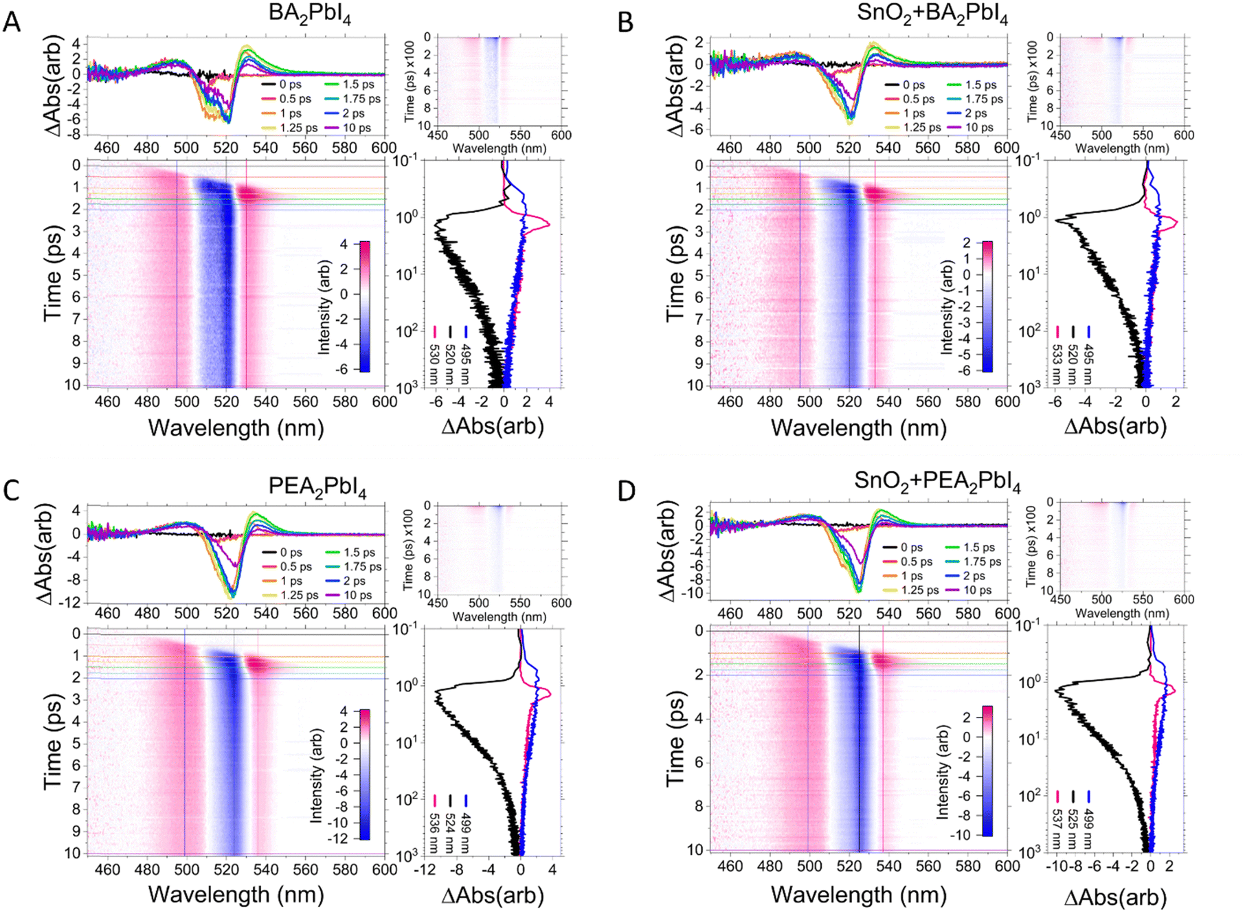 | ||
| Fig. 2 Transient absorption dynamics of (A) BA2PbI4, (B) SnO2/BA2PbI4, (C) PEA2PbI4, and (D) SnO2/PEA2PbI4. In each figure, the bottom left panel shows contour maps of the differential absorption changes as a function of time (y-axis) and wavelength (x-axis) in the early timescale until 10 ps. The top panel shows snapshots of the differential absorption spectrum at different times. The right panel shows the time evolution of each peak, where the blue colour represents the high energy absorption peak, the black line represents the bleaching peak, and the pink line represents the low energy absorption peak over long time delays (∼1000 ps). The top right panel shows the contour lines for longer times. | ||
A common feature present in all samples is an initial redshift of the three peaks: the bleaching signal, and the two absorption features for times <1 ps. This observation agrees well with a theoretical prediction of an excited state geometric relaxation at early times.32 In each case the bleaching signal is longer lived compared with the two absorption features. The decay of each of these three transient species is represented primarily by bimolecular process, details are provided below where we discuss the decay kinetics.
The high energy peak at 495 nm arises due to photoinduced absorption of carriers. The low energy peak at 530 nm decays faster in PEA2PbI4 with an average lifetime of ∼70 ps compared with an average lifetime of ∼111 ps in BA2PbI4, demonstrating the effect of the cation (at pump fluence of 47 μJ cm−2). These decay curves are shown in the ESI† (Fig. S5). The 530 nm peak does not decay to a negative absorption peak with increasing delay time, indicating the absence of biexcitonic features in these samples. As seen in CsPbBr3 NCs, a biexciton decay would result in a bleaching (negative signal) growth due to carrier cooling and recombination processes.21,22 The origin of this low energy TA peak is therefore most likely polaronic since the lifetime depends on the nature of the cation that forms the barrier layer. Moreover, the delay in the appearance of each of the three peaks may be attributed to the inherent nature of each peak. The high energy photoinduced absorption feature (at 495 nm) appears first. The band-edge bleaching signal appears ∼0.5 ps later, indicating the formation of excitons and electron–hole pairs. Consequently, the low energy polaronic absorption peak (at 530 nm) is seen after the band-edge bleaching signal emerges once the excitons dissociate into polarons via exciton–phonon interactions.
While comparing the bleaching signal, it should be noted that BA2PbI4 shows two peaks (Fig. 2A) unlike PEA2PbI4 (Fig. 2B), which shows a single bleaching peak. This is consistent with the steady-state optical results from BA2PbI4 which shows two PL peaks (clearly observed at low temperatures); PEA2PbI4, however, shows a single PL peak from 20–350 K.20 The low energy PL peak in BA2PbI4 was attributed to shallow defects.20 Although the bleaching signal is stronger in PEA2PbI4 compared with BA2PbI4, which is consistent with a stronger PL in PEA2PbI4, the amplitudes of the absorption peaks for both cations are similar. While comparing the perovskite films with and without SnO2 (Fig. 2B and D) the overall TA features remain unchanged; however, the overall amplitude of the two absorption peaks decreases when SnO2 is present. This suggests that even before the thermalization of carriers, there is some transfer of electrons from the conduction band of the perovskite layer to SnO2, similar in both BA2PbI4 and PEA2PbI4.
Fig. 3A–D compares the TA spectra of BA2PbI4 and PEA2PbI4 at selected delay times for four different pump fluences. The data for the SnO2/perovskite heterojunctions are shown in ESI† (Fig. S6). The highest pump fluence of 144 μJ cm−2 corresponds to a carrier density of approximately 4.7 × 1012 cm−2 in PEA2PbI4 (details are provided in ESI†). The overall bleaching intensity increases with the pump fluence for all samples. The intensity of the bleaching peak is larger for the PEA2PbI4 sample compared to the BA2PbI4 sample, although the intensities of the two absorption peaks are comparable at each fluence. The presence of the SnO2 heterojunction does not influence the intensity of the bleaching peak but decreases the intensity of the absorption peaks in both samples at all fluences (Fig. S6, ESI†). The presence of SnO2 further influences the bleaching signal in the SnO2/BA2PbI4 sample by passivating the shallow defect states present only in the BA2PbI4 sample; the two-peak feature of the band-edge bleach is less pronounced in the heterojunction. The ratio of the intensity of the low energy to the high energy absorption peak decreases with increasing pump fluence, whereas at low pump fluence the intensity of the low energy absorption peak is larger compared to that of the high energy absorption peak. This further indicates that the high energy absorption peak at 495 nm is due to the photo-induced absorption of carries since it increases with increasing pump fluence. The low energy absorption peak at 530 nm, however, does not significantly increase with increasing pump fluence.
 | ||
| Fig. 3 Transient absorption spectra as function of pump fluence. The 8-panel figure shows the differential absorption spectra for BA2PbI4 (top) and PEA2PbI4 (bottom) at four pump fluences (A) 47 μJ cm−2, (B) 72 μJ cm−2, (C) 111 μJ cm−2, and (D) 144 μJ cm−2. (E) Schematic of the photoexcitation process. The inset shows a two-particle representation of the excitonic process. | ||
The photoexcitation process is schematically shown in Fig. 3E (using the one particle representation) where a nonthermal distribution of carriers thermalizes to a Fermi Dirac distribution of carriers with an effective temperature of the carriers much higher than that of the lattice. This is then followed by a cooling of the distribution. Due to the presence of excitons in these systems, one should invoke a two-particle representation for excitons, as shown in the inset. A strong coupling between defect traps and hot carriers will result in additional relaxation paths, which may compete with the electron–phonon interaction. The TA data as a function of the pump fluence, which changes the initial carrier concentration, allows us to understand the nature of carrier recombination and the relaxation process. Specifically, it provides insights into whether the dynamics is governed by free carrier and/or exciton relaxation, whether the defect states in BA2PbI4 play a role in the cooling dynamics, and whether the cooling rates depend on the organic cations and the presence of the SnO2 layer.
Decay kinetics
The decay dynamics in hybrid perovskites has been shown to depend on the pump fluence.49,50 Especially in 3D perovskites, high pump fluence implies high charge carrier densities and the recombination involves bimolecular electron–hole and Auger recombination. The overall charge carrier recombination (of the excited state density, n) is usually given by:51 | (1) |
We note that the CVD grown samples have misorientation in the perovskite planes, which reduces the excitonic binding energy, suggesting that these perovskites deviate from a 2D system. These systems are still mainly excitonic; however, the misorientation in the planes as well as defects can result in free carriers at low pump fluences. This in turn suggests that in eqn (1), the first-order term is a tell-tale sign of the presence of excitons in the system and the third-order term signals the presence of free carriers. Additionally, the second-order term may be used to describe the Auger like exciton–exciton annihilation process in an excitonic system and a bimolecular carrier recombination process in the presence of free carriers. It is also important to consider that the formation of bound excitons is not instantaneous. Ultrafast processes in III–V semiconductors,52,53 show a range of time scales with hot e–h pair  cold e–h pair
  continuum exciton
  bound exciton.
In order to make the fitting method unbiased and place the unknown parameters of eqn (1) into comparable (but also intensity dependent) units, we normalize n(t) by its initial value n0, which results in the following equation:
 | (2) |
 | (3) |
![[k with combining tilde]](https://www.rsc.org/images/entities/i_char_006b_0303.gif) 2 = n0k2, and 3 = n02k3, which, due to being in the same units in this form, may be directly compared in determining the dominant decay mechanism for a specific pump fluence.
2 = n0k2, and 3 = n02k3, which, due to being in the same units in this form, may be directly compared in determining the dominant decay mechanism for a specific pump fluence.
The measured intensity counts were fitted by first normalizing n(t), which is to divide by the maximum value n0. The measured intensity counts as a function of time were compared to the solution of the cubic rate eqn (3) by numerical integration. The fit parameters were optimized with multiple nonlinear regression. Notably, the multiple nonlinear regression was relatively straightforward because changing 3, 2, or k1 predominately changes the early, intermediate, and late time behaviour of the integrated solution, respectively. This effective separation of timescales facilitated rapid convergence during the regression process. The differential eqn (3) can be fitted directly with a linear regression; however this requires taking discrete derivatives, which amplify noise. For this reason, fitting to the integrated solution is expected to be more accurate.
Fig. 4A shows the decay kinetics of the normalized bleaching signal as a function of the pump fluence for BA2PbI4 and PEA2PbI4. The bold black and grey lines represent the fits by eqn (3). The data and fits for the perovskite and SnO2 heterojunctions are shown in ESI† (Fig. S7). The decay kinetics depend on the excited state density and the elapsed time. As an example, we show the decay kinetics of PEA2PbI4 at the lowest fluence (47 μJ cm−2) in the three panels of Fig. 4B, where the blue lines illustrate what the fit would look like if only k1, k1 and 2, and all three terms of eqn (3) are considered, respectively. This helps visualize how the rate constants govern at different time scales. As seen, the 3 term impacts early times <10 ps, 2 determines the intermediate times, and k1 dominates at longer times >200 ps. Moreover, the fits demonstrate the need for considering all three rate constants at early times when the system is far from equilibrium. This observation agrees with the earlier discussion that the formation of bound excitons is not instantaneous and at early times the system is not yet excitonic. When the carrier density is high at early times, far from equilibrium, the rate constants are not intrinsic to the material. Only when the excitation density is low, where a dilute exciton gas is maintained, the rate constants are intrinsic to the material and k1 is the dominant term.
 | ||
Fig. 4 Decay of the band-edge bleach. (A) Normalized ΔA of the bleaching signal in BA2PbI4 and PEA2PbI4 and their fits as a function of the pump fluence. (B) Fits to the highest fluence decay data in PEA2PbI4 illustrating the fits when considering only k1 (top panel), k1 and k2 (middle panel), and all three rate constants (bottom panel) of eqn (3). (C) The normalized decay rates  for all four samples as a function of the pump fluence. (D) The un-normalized decay rates for all four samples as a function of the pump fluence. (D) The un-normalized decay rates  for all four samples as a function of the pump fluence. for all four samples as a function of the pump fluence. | ||
1 = k1, 2, and 3 for all four samples versus pump fluence are shown in Fig. 4C. With these normalized units, the y-axis for the three panels is comparable, which demonstrates that the bimolecular (2) and the non-radiative Auger (3) recombination processes dominate the monomolecular process (k1). This further indicates the presence of free carriers in the systems. To further compare the decay rates as a function of the pump fluence across all four samples, we plot the decay rates in un-normalized units: k1, k2, and k3 in Fig. 4D; n0 is taken as the maximum intensity count. Estimation of the absolute carrier density is included in ESI† (Table S2). Several differences are seen between the BA2PbI4 and PEA2PbI4 samples as discussed below.
The presence of defect states in BA2PbI4 (seen as two peaks in the band-edge bleach) impacts the decay rates. The negligible k1 contribution in BA2PbI4 could be more of a fitting artifact due to the scatter in the data beyond 40 ps. The excitonic contribution (k1) is the highest in PEA2PbI4 at higher fluences (top panel of Fig. 4C and D). At high pump fluence, the excited state density increases, and the system behaves like an excitonic system. At the highest pump fluence of 144 μJ cm−2, k1 = 3 × 10⁻³ ps−1 in PEA2PbI4 which is comparable to 2D Sn-based perovskite systems such as PEA2SnI4, where k1 = 2.5 × 10⁻³ ps−1.54 Additionally, this value of k1 is comparable to lifetimes obtained from TRPL measurements (Table S1, ESI†).
Fig. 4D shows that with increasing pump fluence, k3 decreases for all samples and k2 increases, suggesting that the recombination dynamics at higher fluences is mainly governed by monomolecular and bimolecular processes. The highest fluence (144 μJ cm−2) data for PEA2PbI4 fits well with k3 = 0, similar to other excitonic systems where k2 now denotes the exciton–exciton annihilation process due to Auger-like recombination.54 This is contrary to the low fluence data (47 μJ cm−2) for the same sample, where the less-bound e–h pairs play a role with a substantial value for k3, accounting for Auger recombination at early times (Fig. S8, ESI†), further highlighting the role of the excitation density on decay kinetics. BA2PbI4 and its heterojunction with SnO2 at the highest fluence, however does not fit well with k3 = 0, although the value of k3 is lower compared to the low fluence data. This could be related to the defect states in BA2PbI4.
Analysing the decay dynamics shed light on the significance of the three rate constants. At early times, when the excitation density is high and the system is far from equilibrium, the k3 term representing Auger recombination can be significant in such perovskite systems.
Hot carrier cooling
The TA data allows the estimation of the relaxation and cooling dynamics of the photoexcited electron–hole pairs. The normalized TA spectra of all samples at early times (t < 5 ps) after photoexcitation show spectrum broadening at the high-energy tail of the band-edge bleach (insets in Fig. 5). This broadening has been attributed to the presence of a quasi-equilibrium carrier distribution at a temperature larger than the lattice temperature of the sample. The photogenerated carrier distribution upon excitation typically follows a Fermi–Dirac distribution, which may be approximated with Maxwell Boltzmann distribution as long as the excitation energy is much larger than the quasi-Fermi energy13,55| ΔA(ħω) ∝ exp(−ħω/(kBTe)), | (4) |
 | ||
| Fig. 5 Photoexcited carrier cooling. (A) and (B) Transients of cooling curves (carrier temperature), obtained from eqn (4), for all pump fluences for BA2PbI4 and PEA2PbI4, respectively. The dashed lines show fits for an exponential decay in each case. The insets show the normalized TA signal at different time-slices distinguished by different colours and the high-energy tail fits using eqn (4) are shown by dashed black lines. | ||
The carrier temperatures at all pump fluences for BA2PbI4 and PEA2PbI4, extracted from the high-energy tail of the band-edge bleach, are shown in Fig. 5. The carrier temperatures for the heterojunctions are shown in Fig. S10 (ESI†). At the highest pump fluence of 144 μJ cm−2, the initial carrier temperature is close to 2000 K in PEA2PbI4 compared with approximately 1300 K for BA2PbI4. The slightly lower temperatures in BA2PbI4 may be attributed to the defect states, resulting in an energy loss mechanism. The high-energy tail of the second peak at 2.45 eV was fit for the BA2PbI4 (inset, Fig. 5A) sample to obtain the temperatures. At lower fluences, there is more scattering of the data, making it more difficult to fit. By assuming an exponential decay, we obtain the time constant (τc) for the cooling dynamics. The cooling times for the highest pump fluence are shown in Table 1. Overall, the time constants are similar across all samples, ranging between 140–200 fs. At the highest pump fluence of 144 μJ cm−2, slightly enhanced values of τc are observed in the heterojunctions, indicating that electron transfer to the SnO2 layer increases the cooling rates.
| PEA2PbI4 | SnO2/PEA2PbI4 | BA2PbI4 | SnO2/BA2PbI4 | |
|---|---|---|---|---|
| τ c (144 μJ cm−2) | 146 ± 5 fs | 171 ± 10 fs | 157 ± 10 fs | 213 ± 16 fs |
The fast cooling, albeit counterintuitive due to the reduced phonon modes in 2D perovskites, has been observed in several 2D perovskite systems.16,17 This is contrary to 3D MHPs that show longer cooling times, typically in the ∼ps regime, which is mediated by a hot phonon bottleneck effect, especially at high carrier densities.17,56 Ideally, if the electron–phonon interaction is weak, the intrinsic hot carrier lifetime should be long. Using pump–push–probe spectroscopy, Carwithen and co-workers have shown that with increased binding energy of the excitons, the suppression of the hot phonon bottleneck becomes more pronounced, resulting in faster cooling rates.17 The fast cooling rates here indicates that the Fröhlich interaction plays a major role. What is perhaps surprising is that both BA2PbI4 and PEA2PbI4 show similar τc, even though BA2PbI4 has defect states (Fig. 2). These results suggest that defects play less of a role in the relaxation process in 2D MHPs and that the main driving factor is the carrier–phonon interaction, which is less screened in 2D perovskites due to the low dielectric function of the organic barrier layer. Although fast cooling rates are not ideal for photovoltaic materials, our results provide insights into the role of organic cations in carrier cooling. Additionally, since CVD is such a versatile process for the growth of 2D perovskites and for tailoring the orientation of the perovskite planes by changing the initial thickness of the metal halide layer, it opens a vast space for tuning carrier dynamics in 2D MHPs as a function of the thickness of the films and the type of organic cations.
Conclusions
In summary, we present ultrafast TA spectroscopy from CVD grown 2D MHPs using the prototypes BA2PbI4 and PEA2PbI4. The heterojunctions of these films with a thin spin coated SnO2 layer were also investigated. The TA features are characterized by a low and a high energy absorption peak with respect to the band-edge bleach at 520 nm. The low energy absorption peak at 530 nm decays faster in PEA2PbI4 (70 ps) compared with BA2PbI4, (111 ps) indicating that the cation plays a role. It is most likely polaronic in nature where the absorption peak denotes optical excitation of the polaron due to the organic cation.The decay dynamics of the band-edge bleach as a function of the pump-fluence was investigated in a way that is not fully accounted for in the literature. For low to intermediate pump fluence, the decay in all samples fits best with three rate constants. At early times when the carrier density is high and the system is far from equilibrium, the Auger recombination (k3) is the dominant term as the less bound e–h pairs can interact with each other. As time elapses, when a dilute exciton gas is formed, the decay is mainly determined by a single parameter (k1). Subtle differences are seen between PEA2PbI4 and BA2PbI4 at high pump fluences. The k3 term vanishes in PEA2PbI4 at the highest fluence when the exciton population is high, and the bimolecular term dominates. Although the k3 term decreases in BA2PbI4 with increasing fluence but it is finite, which is most likely due to the defect states.
At the same pump fluence, the hot carrier Fermi temperature is higher in PEA2PbI4 compared with BA2PbI4, which we attribute to defect states in BA2PbI4 resulting in additional energy loss in the thermalization process. Despite the differences in defect states and the Auger recombination contribution in PEA2PbI4 and BA2PbI4, the carrier cooling times in both samples are almost identical (∼150 fs). This fast-cooling rate suggests that the main driving component here is the Fröhlich interaction term. The feasibility of the growth of compact 2D perovskites films by CVD allows a glimpse into how the growth method itself plays a role in the electronic properties and thus, carrier dynamics in these systems along with the versatility for tuning material properties.
Author contributions
SG and PY conceived the work. DB, PY, and SG set up the transient absorption measurement system. DB and SG synthesized the samples. DB conducted optical experiments and analysed the data. DH was involved with decay kinetics analysis and simulations. The manuscript was written by SG and DB with contributions from all authors. All authors have given approval to the final version of the manuscript.Data availability
The data supporting the findings of this study are available within the article and/or have been included as part of its ESI.†Conflicts of interest
There are no conflicts to declare.Acknowledgements
We acknowledge the support of the instrumentation obtained through the National Science Foundation (NSF) under Grant No. ECCS-1872846. PY and SG acknowledge the University of Missouri Material Science and Engineering Institute Seed Grant No. CD002233. We thank Randy Burns and Chris Arendse for help with the CVD growth of the perovskite films and Carsten Ullrich for valuable discussions.Notes and references
- NREL, 2024, https://www.nrel.gov/pv/cell-efficiency.html.
- L. N. Quan, B. P. Rand, R. H. Friend, S. G. Mhaisalkar, T.-W. Lee and E. H. Sargent, Chem. Rev., 2019, 119, 7444–7477 CrossRef CAS PubMed.
- Q. Zhang, Q. Shang, R. Su, T. T. H. Do and Q. Xiong, Nano Lett., 2021, 21, 1903–1914 CrossRef CAS.
- Y. Zhou, Y. Huang, X. Xu, Z. Fan, J. B. Khurgin and Q. Xiong, Appl. Phys. Rev., 2020, 7, 041313 CAS.
- J. Xu, X. Li, J. Xiong, C. Yuan, S. Semin, T. Rasing and X.-H. Bu, Adv. Mater., 2020, 32, 1806736 CrossRef CAS.
- Y. Zhou, J. Chen, O. M. Bakr and O. F. Mohammed, ACS Energy Lett., 2021, 6, 739–768 CrossRef CAS.
- T. Yang, F. Li and R. Zheng, ACS Appl. Electron. Mater., 2019, 1, 1348–1366 CrossRef CAS.
- C. C. Stoumpos, D. H. Cao, D. J. Clark, J. Young, J. M. Rondinelli, J. I. Jang, J. T. Hupp and M. G. Kanatzidis, Chem. Mater., 2016, 28, 2852–2867 CrossRef CAS.
- M. D. Smith, B. A. Connor and H. I. Karunadasa, Chem. Rev., 2019, 119, 3104–3139 CrossRef CAS.
- Y.-T. Li, L. Han, H. Liu, K. Sun, D. Luo, X.-L. Guo, D.-L. Yu and T.-L. Ren, ACS Appl. Electron. Mater., 2022, 4, 547–567 CrossRef CAS.
- L. Mao, W. Ke, L. Pedesseau, Y. Wu, C. Katan, J. Even, M. R. Wasielewski, C. C. Stoumpos and M. G. Kanatzidis, J. Am. Chem. Soc., 2018, 140, 3775–3783 CrossRef CAS.
- J. C. Blancon, A. V. Stier, H. Tsai, W. Nie, C. C. Stoumpos, B. Traoré, L. Pedesseau, M. Kepenekian, F. Katsutani, G. T. Noe, J. Kono, S. Tretiak, S. A. Crooker, C. Katan, M. G. Kanatzidis, J. J. Crochet, J. Even and A. D. Mohite, Nat. Commun., 2018, 9, 2254 CrossRef PubMed.
- Q. Chang, D. Bao, B. Chen, H. Hu, X. Chen, H. Sun, Y. M. Lam, J.-X. Zhu, D. Zhao and E. E. M. Chia, Commun. Phys., 2022, 5, 187 CrossRef CAS.
- J. M. Richter, F. Branchi, F. Valduga de Almeida Camargo, B. Zhao, R. H. Friend, G. Cerullo and F. Deschler, Nat. Commun., 2017, 8, 376 CrossRef PubMed.
- J. Fu, Q. Xu, G. Han, B. Wu, C. H. A. Huan, M. L. Leek and T. C. Sum, Nat. Commun., 2017, 8, 1300 CrossRef PubMed.
- V. A. Hintermayr, L. Polavarapu, A. S. Urban and J. Feldmann, ACS Nano, 2018, 12, 10151–10158 CrossRef CAS.
- B. P. Carwithen, T. R. Hopper, Z. Ge, N. Mondal, T. Wang, R. Mazlumian, X. Zheng, F. Krieg, F. Montanarella, G. Nedelcu, M. Kroll, M. A. Siguan, J. M. Frost, K. Leo, Y. Vaynzof, M. I. Bodnarchuk, M. V. Kovalenko and A. A. Bakulin, ACS Nano, 2023, 17, 6638–6648 CrossRef CAS PubMed.
- J. Zhang, X. Zhu, M. Wang and B. Hu, Nat. Commun., 2020, 11, 2618 CrossRef CAS PubMed.
- S. Deng, E. Shi, L. Yuan, L. Jin, L. Dou and L. Huang, Nat. Commun., 2020, 11, 664 CrossRef CAS.
- C. J. Arendse, R. Burns, D. Beckwitt, D. Babaian, S. Klue, D. Stalla, E. Karapetrova, P. F. Miceli and S. Guha, ACS Appl. Mater. Interfaces, 2023, 15, 59055–59065 CrossRef CAS.
- J. Aneesh, A. Swarnkar, V. Kumar Ravi, R. Sharma, A. Nag and K. V. Adarsh, J. Phys. Chem. C, 2017, 121, 4734–4739 CrossRef CAS.
- A. Shukla, G. Kaur, K. J. Babu, N. Ghorai, T. Goswami, A. Kaur and H. N. Ghosh, J. Phys. Chem. Lett., 2020, 11, 6344–6352 CrossRef CAS PubMed.
- D. Seyitliyev, X. Qin, M. K. Jana, S. M. Janke, X. Zhong, W. You, D. B. Mitzi, V. Blum and K. Gundogdu, Adv. Funct. Mater., 2023, 33, 2213021 CrossRef CAS.
- C. D. Sonnichsen, D. P. Strandell, P. J. Brosseau and P. Kambhampati, Phys. Rev. Res., 2021, 3, 023147 CrossRef CAS.
- N. Yarita, H. Tahara, T. Ihara, T. Kawawaki, R. Sato, M. Saruyama, T. Teranishi and Y. Kanemitsu, J. Phys. Chem. Lett., 2017, 8, 1413–1418 CrossRef CAS.
- J. B. Hoffman, A. L. Schleper and P. V. Kamat, J. Am. Chem. Soc., 2016, 138, 8603–8611 CrossRef CAS PubMed.
- K. Wei, X. Zheng, X. Cheng, C. Shen and T. Jiang, Adv. Opt. Mater., 2016, 4, 1993–1997 CrossRef CAS.
- J. Wang, T. Ding, J. Leng, S. Jin and K. Wu, J. Phys. Chem. Lett., 2018, 9, 3372–3377 CrossRef CAS.
- A. M. A. Leguy, P. Azarhoosh, M. I. Alonso, M. Campoy-Quiles, O. J. Weber, J. Yao, D. Bryant, M. T. Weller, J. Nelson, A. Walsh, M. van Schilfgaarde and P. R. F. Barnes, Nanoscale, 2016, 8, 6317–6327 RSC.
- S. G. Motti, M. Kober-Czerny, M. Righetto, P. Holzhey, J. Smith, H. Kraus, H. J. Snaith, M. B. Johnston and L. M. Herz, Adv. Funct. Mater., 2023, 33, 2300363 CrossRef CAS.
- J. Lu, W. Chen, C. Zhou, S. Yang, C. Wang, R. Wang, X. Wang, Z. Gan, B. Jia and X. Wen, J. Mater. Chem. C, 2021, 9, 8966–8974 RSC.
- A. Boziki, P. Baudin, E. Liberatore, N. Ashari Astani and U. Rothlisberger, J. Comput. Chem., 2022, 43, 577–582 CrossRef CAS.
- A. D. Taylor, Q. Sun, K. P. Goetz, Q. An, T. Schramm, Y. Hofstetter, M. Litterst, F. Paulus and Y. Vaynzof, Nat. Commun., 2021, 12, 1878 CrossRef CAS.
- P. Luo, Z. Liu, W. Xia, C. Yuan, J. Cheng and Y. Lu, ACS Appl. Mater. Interfaces, 2015, 7, 2708–2714 CrossRef CAS PubMed.
- M. R. Leyden, L. K. Ono, S. R. Raga, Y. Kato, S. Wang and Y. Qi, J. Mater. Chem. A, 2014, 2, 18742–18745 RSC.
- M. M. Tavakoli, L. Gu, Y. Gao, C. Reckmeier, J. He, A. L. Rogach, Y. Yao and Z. Fan, Sci. Rep., 2015, 5, 14083 CrossRef.
- S. Ngqoloda, C. J. Arendse, T. F. Muller, P. F. Miceli, S. Guha, L. Mostert and C. J. Oliphant, ACS Appl. Energy Mater., 2020, 3, 2350–2359 CrossRef CAS.
- R. Burns, S. Ngqoloda, S. C. Klue, E. Karapetrova, C. J. Arendse and S. Guha, ACS Appl. Electron. Mater., 2022, 4, 4258–4264 CrossRef CAS.
- S. Kahmann, H. Duim, H.-H. Fang, M. Dyksik, S. Adjokatse, M. Rivera Medina, M. Pitaro, P. Plochocka and M. A. Loi, Adv. Funct. Mater., 2021, 31, 2103778 CrossRef CAS.
- R. Chakraborty and A. Nag, J. Phys. Chem. C, 2020, 124, 16177–16185 CrossRef CAS.
- A. Shkarin, AlexShkarin/pyLabLib: Update to 1.4.2, 2023 DOI:10.5281/zenodo.8418353.
- M. V. Morrell, A. Pickett, P. Bhattacharya, S. Guha and Y. Xing, ACS Appl. Mater. Interfaces, 2021, 13, 38579–38585 CrossRef CAS.
- P. Lefebvre, P. Christol and H. Mathieu, Phys. Rev. B: Condens. Matter Mater. Phys., 1993, 48, 17308–17315 CrossRef CAS PubMed.
- K. Momma and F. Izumi, J. Appl. Crystallogr., 2011, 44, 1272–1276 CrossRef CAS.
- R. Butler, R. Burns, D. Babaian, M. J. Anderson, C. A. Ullrich, M. V. Morrell, Y. Xing, J. Lee, P. Yu and S. Guha, J. Appl. Phys., 2022, 131, 125105 CrossRef CAS.
- D. Shin, F. Zu, E. R. Nandayapa, L. Frohloff, E. Albert, E. J. W. List-Kratochvil and N. Koch, Adv. Funct. Mater., 2023, 33, 2208980 CrossRef CAS.
- S. Silver, J. Yin, H. Li, J.-L. Brédas and A. Kahn, Adv. Energy Mater., 2018, 8, 1703468 CrossRef.
- J. Gong, Y. Cui, F. Li and M. Liu, Small Sci., 2023, 3, 2200108 CrossRef CAS.
- M. B. Johnston and L. M. Herz, Acc. Chem. Res., 2016, 49, 146–154 CrossRef CAS PubMed.
- B. A. Chen, G. T. Pang, X. Q. Lan, Z. B. He and R. Chen, Mater. Today Phys., 2020, 14, 100228 CrossRef.
- C. Wehrenfennig, M. Liu, H. J. Snaith, M. B. Johnston and L. M. Herz, Energy Environ. Sci., 2014, 7, 2269–2275 RSC.
- J. Shah, B. Deveaud, T. C. Damen, W. T. Tsang, A. C. Gossard and P. Lugli, Phys. Rev. Lett., 1987, 59, 2222–2225 CrossRef CAS PubMed.
- A. V. Nurmikko, in Semiconductors and Semimetals, ed. D. G. Seiler and C. L. Littler, Elsevier, 1992, vol. 36, pp. 85–135 Search PubMed.
- T. Zhang, C. Zhou, J. Lin and J. Wang, ACS Photonics, 2022, 9, 1627–1637 CrossRef CAS.
- M. B. Price, J. Butkus, T. C. Jellicoe, A. Sadhanala, A. Briane, J. E. Halpert, K. Broch, J. M. Hodgkiss, R. H. Friend and F. Deschler, Nat. Commun., 2015, 6, 8420 CrossRef CAS.
- L. Dai, J. Ye and N. C. Greenham, Light: Sci. Appl., 2023, 12, 208 CrossRef CAS PubMed.
Footnote |
| † Electronic supplementary information (ESI) available: CVD growth of 2D perovskites; pump–probe spectroscopy setup; time-resolved photoluminescence fits; generalized Elliot model for absorption; carrier density estimation; transient absorption spectra from a 50 nm thick PEA2PbI4 film and SnO2/perovskite heterojunctions; decay curves of the low energy absorption peak; decay fits at different fluences; method for extracting carrier temperature; hot carrier cooling in SnO2/perovskites. See DOI: https://doi.org/10.1039/d4tc03014a |
| This journal is © The Royal Society of Chemistry 2025 |