
 Open Access Article
 This Open Access Article is licensed under a Creative Commons Attribution-Non Commercial 3.0 Unported Licence
Intense pulsed light annealing of CdS and Au-decorated CdS nanoparticles for high-performance, self-powered silicon-based heterojunction photodetectors
Hadeel F. Abbasa,
Raid A. Ismail *a,
Walid K. Hamoudib and
Mayyadah H. Mohsina
*a,
Walid K. Hamoudib and
Mayyadah H. Mohsina
aCollege of Applied Science, University of Technology, Baghdad, Iraq
bAl-Farabi University, Baghdad, Iraq. E-mail: raidismail@yahoo.com
First published on 4th July 2025
Abstract
The enhancement of visible light responsivity in nanostructured heterojunction silicon photodetectors has attracted significant research interest. In this work, intense pulsed light (IPL) annealing was employed to improve the performance of CdS/Si and Au-decorated CdS/Si photodetectors fabricated via laser ablation. X-ray diffraction (XRD) confirms a substantial improvement in crystallinity of both CdS and Au-decorated CdS after IPL annealing. The particle size of the CdS increased from 78 to 100 nm and from 10 to 15 nm for Au-decorated CdS after annealing. The mobility of the CdS and Au-decorated CdS increases after annealing. The optical energy gap of CdS increases from 2.55 to 2.68 eV after annealing. Photoluminescence studies of CdS nanoparticles after annealing show the presence of an intense single peak at 450 nm. Structural and optical analyses reveal that IPL annealing reduced defects and enlarged the depletion layer width, giving a twofold responsivity increase from 0.19 to 0.36 A W−1 at 520 nm for CdS/Si and 0.23 to 0.42 A W−1 at 460 nm for Au-decorated CdS/Si. The obtained results indicated that IPL annealing was rapid and optimized heterojunction photodetectors. The energy band diagram of Au-decorated CdS/Si after annealing was constructed under illumination. The effect of aging time on the performance of the fabricated photodetectors was investigated.
1. Introduction
Cadmium sulfide (CdS) is one of the most important semiconductors due to its attractive optical and electrical properties that facilitate its widespread use in many technological and industrial applications. Crystalline CdS is an n-type semiconductor with an energy gap ranging between 2.42 and 2.45 eV at room temperature. CdS nanoparticles drew significant attention due to their excellent physical and chemical properties.1 They were used as photocatalysts, solar cells, heterojunction photodetectors, light-emitting diodes, bio-imaging, gas sensors, switching memory, etc.2–5 Noble metal–semiconductor core–shell (C–S) nanoparticles are attractive too due to their distinctive electrical properties, optical absorption, high wavelength selectivity, stability, chemical resistance, and large surface area.6,7The size and morphology of the CdS nanoparticles can manipulate their optical and electrical properties.8 CdS can be found in different morphologies, such as nanoparticles, nanowires, nanorods, nanotubes, nanosheets, nanobelts and nanoflowers.9–11 Various preparation methods have been used to synthesize CdS nanomaterials; among them are: chemical vapor deposition CVD, hydrothermal, solvothermal, liquid exfoliation, template-assisted growth,12 electrodeposition, and laser ablation in liquid (LAL).9,12–14 The latter offers many advantages as a route for producing nanomaterials, such as simplicity, eco-friendliness, a one-step process, low-cost, nearly stoichiometric, fair size control, no need for vacuum or a catalyst, synthesizing metal oxides, and producing pure nanomaterials.2 A CdS-based silicon heterojunction photodetector prepared by laser ablation in liquid has drawn significant interest due to its superior optoelectronic properties compared to those fabricated by other techniques.15,16
Synthesis-based core/shell structure was found to be promising and attractive during the improvement of the optical and electrical properties of the CdS nanoparticles. The shell can play an important role in the reduction of the non-radiative recombination by passivating defects levels at the CdS surface and it can improve the photoluminescence properties of the CdS. Furthermore, this shell can act as a source to passivate the surface traps, prevent oxidation, and enhance chemical stability of the core CdS nanoparticles.17
For heterojunction photodetectors, the core/shell morphology results in tuning of the band alignment of the two semiconducting materials. This consequently enhances the photogenerated carrier's separation and transport. Many core/shell structure-based CdS nanoparticles have been reported such as TiO2/CdS, ZnO/CdS, CdS/PbS, etc.18–20
Intense pulse light IPL annealing is a promising, rapid surface treatment technique to enhance the performance of semiconducting films and devices by reducing structural defects and mechanical stresses. As compared to conventional heat treatment methods, IPL annealing is cost-effective, enables short-time annealing, provides high selectivity for surface treatment, requires low thermal budget, allows large-area processing, and minimizes dopant diffusion.21
Herein, we report on the improvement of photoresponse properties of CdS NPs/Si and Au-decorated CdS/Si core–shell photodetectors synthesized by low-cost laser ablation in liquid and spin coating by rapid annealing using the intense pulse light technique.
2. Experimental procedure
Every chemical utilized in this experiment was reagent grade and did not require any additional purification. High-purity Cd pellets (99.99%) placed in glass vessels filled with thiourea solution were laser-ablated to create CdS nanoparticles using a Q-switched Nd:YAG laser set to 1064 nm wavelength and 7 ns pulse duration. The laser beam was focused onto the Cd pellet using a 12 cm converging lens. The ablation solution was prepared by mixing 10 mM thiourea (CH4N2S) as a sulfur source with 50% ethanol (used here to prevent CdO formation) and 3.57 mM cetyltrimethylammonium bromide CTAB [(C16H33)N(CH3)3]Br as a surfactant. Laser ablation was performed using 200 shots at a fluence of 3 J cm−2, as shown in Fig. 1a. The ablation time was 15 minutes. The laser spot diameter on the Cd target was 500 μm, as determined by an optical microscope, and the solution level was set at 2 mm above the Cd pellet. To synthesize Au-decorated CdS, a gold pellet (shell) was ablated in colloidal CdS NPs (core) using 140 laser pulses from the fundamental wavelength (λ = 1064 nm) Nd:YAG laser by using 4.5 J cm−2 laser fluence and 7 ns duration, as shown in Fig. 1b. The structural properties of CdS and Au-decorated CdS nanoparticles were examined using X-ray diffractometer (XRD-6000, Shimadzu). The morphology and particle size of the product were investigated using scanning electron microscope SEM (FE-SEM; MIRA3 TESCAN) and transmission electron microscope TEM (CM10 pw6020). The vibration modes of the nanoparticles were determined using Raman spectroscopy (Bruker Raman microscope). The infrared absorption of the colloidal nanoparticles was measured using Fourier transformed infrared FT-IR (Shimadzu 8000 spectrometer). The optical absorption of the CdS and Au-decorated CdS nanoparticles were investigated using UV-vis spectrophotometer (Shimadzu, 00912901-S). The electrical resistivity and mobility of the nanoparticles were measured using Hall effect. The spin coating was employed to deposit the CdS and Au-decorated CdS films on cleaned glass and 500 μm-thick n-type (111) mirror-like single-crystalline silicon substrates having electrical resistivity of 3–5 Ω cm. To carry out the annealing process, 100 light pulses at 2 J cm−2 fluence and 3 ms duration of a laboratory-assembled intense pulse light (IPL) system were used to anneal the CdS and Au-decorated CdS films. | ||
| Fig. 1 (a) Schematic diagram of preparation of CdS NPs and Au-decorated CdS and (b) experimental steps of fabrication of CdS/Si and Au-decorated CdS/Si photodetectors. | ||
Ohmic contacts were made by evaporating a thick aluminum film on the backside of the silicon and an indium film on the CdS and Au@CdS films through a mask, as shown in Fig. 1b. Current–voltage characteristics under dark conditions were measured using a digital DC power source and an electrometer. Capacitance–voltage characteristics at reverse bias were measured using an LCR meter at a frequency of 200 kHz. An assessment photodetector system, which includes a Jobin Yvon monochromator, halogen lamp, beam splitter, converging lens, silicon power meter (Sanwa), and electrometer, was used to measure the photodetectors' responsivity.
3. Results and discussion
Fig. 2 shows the XRD patterns of CdS NPs and Au-decorated CdS films deposited on glass substrates before and after IPL annealing. Before annealing, the XRD pattern of Fig. 2a shows the presence of a single peak located at 2θ = 43.6°, corresponding to the (110) plane. After annealing, the XRD pattern exhibits the formation of two extra peaks positioned at 2θ = 25.5° and 26.5°, corresponding to (002) and (101) planes, respectively.22 These new peaks belong to the crystalline hexagonal CdS, according to JCPDs # 41-1049.23 This finding has resulted because of the structural defects recovery and is attributed to the crystallinity improvement of the films after annealing. A brief round of annealing has given the grains the thermal energy they need to shift and redistribute into a more ordered structure. Despite that, the concentrated residual stresses accompanying the laser ablation may decrease after the IPL annealing. The crystallite size of CdS, calculated from the Scherrer equation, increased from 79 nm to 90 nm after annealing. Fig. 2b shows. The XRD pattern of Au-decorated CdS before and after IPL. Before IPL annealing, the XRD of Au-decorated CdS film exhibits four peaks, two of which are related to hexagonal CdS, and the other two are located at 2θ = 38° and 44.4°, corresponding to (111) and (200) planes, respectively, which belong to the Au shell.24 After IPL annealing, the intensity of the XRD peaks increased slightly while their full width at half maximum decreased because of the reduction of defects and strain. The average nanoparticle size increased from 67 to 120 nm after annealing, which is consistent with the XRD results. A few larger CdS particles were also observed after annealing. Similar outcomes were obtained for Au-decorated CdS, as shown in Fig. 3c and d, where the SEM image prior to annealing showed spherical nanoparticles and a small number of nanowires. The average particle size of the Au-decorated CdS increased from 78 to 100 nm after annealing. Fig. 3e–g show the TEM images of Au-decorated CdS, which confirm the formation of core–shell morphology, where the black regions refer to the CdS and the gray ones refer to the Au decoration. | ||
| Fig. 2 (a) X-ray diffraction of CdS film before and after annealing and (b) X-ray diffraction of Au-decorated CdS film before and after annealing. | ||
 | ||
| Fig. 3 (a–d) SEM images of CdS and Au-decorated CdS before and after IPL annealing, (e–g) TEM images of Au-decorated CdS nanoparticles, and (h and i) particle size distribution histograms. | ||
Compared to conventional furnace annealing, IPL annealing has offered rapid, high-intensity, and localized heating within milliseconds. This has enabled effective sintering and grain growth while minimizing thermal damage to the substrate and reducing the overall processing time and energy consumption. The SEM images of CdS nanoparticles before annealing (Fig. 3a and b) reveal well-dispersed, nearly spherical particles with narrow size distribution. After annealing, an increased particle size and partial coalescence were seen as a result of particle mobility and fusion driven by localized heating, as shown in (Fig. 3c & d). This has led to results with less distinct boundaries and some clustering. The improved particle connectivity and increased grain size are expected to reduce grain boundary defects and enhance charge transport properties, which are needed in optoelectronics applications such as photovoltaic devices and sensors.25
The average size of Au-decorated CdS increased from 10 to 15 nm after annealing, and no effect of the annealing was observed on morphology (Fig. 3e & f). This size increase is attributed to the sintering that occurs during annealing, where particles undergo coalescence or growth mechanisms. The formation of nanowires in Au-decorated CdS is due to the strongly confined plasma generated by the surrounding liquid during laser ablation9 and shown in the TEM image of Fig. 3f. This has promoted anisotropic (1D) growth and changed the cooling dynamics. Instead of isotropic nanoparticles, such confinement may encourage atoms to bind orientedly to produce nanowires.22 The particle size distribution (Fig. 3h & k) of Au-decorated CdS after annealing was found to be wider than before annealing, suggesting potential sintering effects.
Fig. 4a shows the UV-vis a decreasing absorption of CdS film with increasing wavelength and tends to saturate at λ = 495 nm, corresponding to the absorption edge of CdS. This decrease is due to the nanoparticles' agglomeration reduction. Contrarily, the particle size has increased and led to a reduction of light scattering.26 The optical energy gap of CdS before and after annealing was determined by plotting the variation of (αhν)2 with photon energy (hν), as shown in Fig. 4b. The extrapolation of the linear part on the photon energy axis provided the optical energy gaps, which were 2.55 eV before annealing and became 2.68 eV after annealing. This increase of the energy gap is attributed to the improved film crystallinity, which was induced by a decrease in the structural defects as well as by the enhancement of film stoichiometry.27 CdS film with a high oxygen or sulfur content exhibited a lower energy gap. The UV-vis absorption plots of Au-decorated CdS films before and after annealing are shown in Fig. 4c. The optical absorption decreased as the wavelength increased, and a small absorption peak was observed at 525 nm.
 | ||
| Fig. 4 (a) UV-vis absorption spectra of CdS films before and after annealing, (b) (αhν)2 versus photon energy plot of CdS, (c) UV-vis absorption spectra of Au-decorated CdS films before and after annealing, and (d) (αhν) 2 against photon energy plot of Au-decorated CdS. | ||
The peak, which shows electron oscillation in the Au shell NPs, may have been caused by the Au NPs' surface plasmon resonance (SPR) effect. This is thought to be the key reason for enhancing the responsivity of the Au-decorated CdS/Si photodetector at this specific wavelength. Similarly, the optical energy gap of Au-decorated CdS was determined from Fig. 4d and found to be 2.46 and 2.65 eV, respectively, before and after annealing. The energy gap of CdS NPs was found to be larger than the Au-decorated CdS where the formation of a shell by Au around CdS NPs leads to an electronic interaction and plasmonic coupling, which reduces the CdS energy gap. The charge transfer from the Au shell to CdS, as well as the damping of quantum confinement (due to the metallic environment), can play strong roles in reducing the energy gap of CdS when it is covered with an Au shell.28,29
The photoluminescence emission (PL) spectra of CdS and Au-decorated CdS before and after IPL annealing are shown in Fig. 5a and b. Band-to-band recombination is represented by a tiny emission peak at 460 nm (2.69 eV) in the PL spectra prior to annealing.30 After IPL annealing, the intensity of the PL peak increased remarkably, as shown in Fig. 5a. This is due to the passivation of the surface trap states and to the formation of dangling bonds during laser ablation after facilitating oxygen atoms' interaction with the CdS NPs and Au shell surfaces. This in turn reduced the non-radiative recombination NRR and increased the radiative recombination, giving stronger PL intensity.28,31
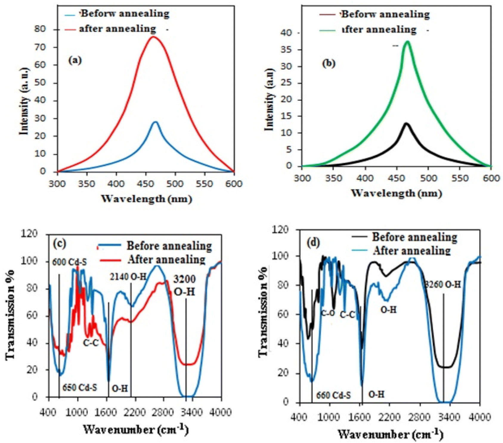 | ||
| Fig. 5 (a) PL spectra of CdS NPs before and after annealing, (b) PL spectra of Au-decorated CdS, (c) FT-IR spectrum of CdS before and after annealing, and (d) FT-IR spectrum of Au-decorated CdS before and after annealing. | ||
Fig. 5(c & d) shows the FT-IR spectra of CdS NPs and Au-decorated CdS structures before and after IPL annealing. Key absorption peaks are observed in the range 600–680 cm−1, corresponding to Cd–S stretching vibrations from the CdS lattice. The peak at ∼650 cm−1 (Cd–S) shifts to ∼665 cm−1 after IPL annealing, indicating enhanced crystallinity as a result of reduced lattice strain and defect passivation.32 The broad peak at ∼3400 cm−1 (O–H stretching) and the shoulder at ∼1600 cm−1 (H–O–H bending) confirm adsorbed water on the NPs' surface. After annealing, these peaks weakened significantly, suggesting desorption of surface moisture due to IPL-induced heating. Peaks at 1100 cm−1 (C–O) and 1300 cm−1 (C–C), attributed to residual thiourea from synthesis,32 diminished/vanished post-annealing, confirming thermal decomposition of the organic residues. The shift in Cd–S vibration (650 → 665 cm−1) and the reduction in FWHM (full width at half maximum) of this peak reflect improved atomic ordering, consistent with XRD results (Fig. 2). Au-decorated CdS showed a similar peak sharpening but a smaller shift (648 → 658 cm−1), most likely because Au stabilizes the CdS lattice.33 These changes correlate with the enhanced photodetector performance (Fig. 6), as the reduced surface defects have suppressed charge recombination. To better contextualize our results, Table 1 compares the structural, optical, and electronic characteristics of Au-decorated CdS nanostructures reported in the literature with those obtained in this work.
 | ||
| Fig. 6 (a) Dark I–V characteristics of CdS/Si heterojunction before and after annealing, (b) dark I–V characteristics of Au-decorated CdS/Si heterojunction before and after annealing, (c) I–V characteristics of CdS/Si under illumination before and after annealing, and (d) I–V characteristics of Au-decorated CdS/Si under illumination before and after annealing. | ||
| Reference | Synthesis method | Annealing method | Crystallinity/phase | Crystallite size (nm) | Energy gap (eV) | PL intensity |
|---|---|---|---|---|---|---|
| This work | Laser ablation in liquid (LAL) | IPL annealing (rapid, localized) | Enhanced (hexagonal CdS peaks sharpened) | ↑ from 67 to 120 | CdS: ↑ from 2.55 → 2.68 | Strong (450 nm peak after annealing) |
| Au-decorated CdS: 2.46 → 2.65 | ||||||
| 34 | Colloidal deposition | Furnace (300–550 °C) | Shell sintering into the matrix, continuous CdS | From 4 to 6 | Red shift in PL due to shell merging | Shifted, broadened PL |
| 35 | Stepwise colloidal method | No post-annealing | Core–shell-rod hybrid structure | From 1.38 to 5.62 | Broad absorption (400–850 nm)— | Strong SPR in Au core |
| 36 | Chemical bath deposition (CBD) | Thermal annealing | CdS cubic with (111) preferred orientation | From 5 to 70 | ↑ with thickness | Moderate |
| ↓ after annealing |
All of the CdS and Au-decorated CdS samples displayed n-type conductivity, according to Hall measurements. After annealing, the CdS layer's electrical resistivity dropped from 1.763 × 10⁵ to 1.1 × 10⁵ Ω cm. This is due to the drop in structural defects and the improved CdS film stoichiometry, as well as the enhanced carrier mobility after annealing, as shown in Table 2. The electrical resistivity of Au-decorated CdS samples showed a decrease while their mobility increased after annealing.32 These behaviors could be explained as follows: when the IPL light was absorbed by the Au shell, it exhibited localized plasmonic resonance (LPR), which increased the carrier density in the CdS conduction band and reduced the carriers' recombination. Furthermore, it's possible that the annealing reduced the aggregation of Au nanoparticles, which could have served as recombination sites.33,37
| Sample | Condition | Resistivity (Ω cm) | Mobility (cm3 V−1 s−1) |
|---|---|---|---|
| CdS | Before annealing | 1.763 × 10⁵ | 141.54 |
| After annealing | 1.1 × 10⁵ | 144.56 | |
| Au-decorated CdS | Before annealing | 2.599 × 10⁴ | 1.158 × 10² |
| After annealing | 1.918 × 10⁴ | 1.718 × 10³ |
The current–voltage characteristics of CdS/Si and Au-decorated CdS/Si heterojunction photodetectors under dark and illumination at room temperature are depicted in Fig. 6. The I–V characteristics in the voltage range −5 to +5 V before and after annealing showed a rectifying behavior. The forward current of the CdS/Si heterojunction increased exponentially with bias voltage, which reflects the domination of diffusion current over the recombination current at bias voltage >3 V.38,39 This forward current increased after annealing due to the decreased structural defects and surface states, as well as the nanoparticle agglomeration (Fig. 6a).40–42
The Au-decorated CdS/Si heterojunction forward current also rose exponentially with bias voltage, confirming the current transport mechanism's compliance with the basic diode equation (Fig. 6b). The forward current of Au-decorated CdS/Si heterojunction is larger than the CdS/Si due to the presence of the Au shell, which decreased the electrical resistivity of the CdS core.43
The ideality factor (n) of the heterojunction was calculated using the following equation:
 | (1) |
| Condition | Photodetector type | Ideality factor |
|---|---|---|
| Before IPL annealing | CdS/Si | 2.89 |
| After IPL annealing | CdS/Si | 2 |
| Before IPL annealing | Au-decorated CdS/Si | 1.9 |
| After IPL annealing | Au-decorated CdS/Si | 1.83 |
The ideality factor improvement after annealing, for both heterojunctions, is attributed to the reduction of series resistance and saturation current after annealing. A value of ideality factor greater than unity indicates the presence of surface states and traps at the interface.40,44,45 Fig. 6c & d shows the illuminated I–V characteristics of CdS/Si and Au-decorated CdS/Si heterojunctions before and after annealing. The photocurrent of the Au-decorated CdS/Si heterojunction is larger than the CdS/Si heterojunction. This is explained by the Au shell's presence, which served as an electron source to offset electron recombination and raise the number of photogenerated carriers. The photocurrent of both heterojunctions increased after annealing because of the decreased concentration of the recombination centers and the increased diffusion length of the carriers. This has taken place because of the reduced grain boundaries as well as the increased grain size of the CdS and Au-decorated CdS.44
The Au-decorated CdS/Si photodetectors' photo detection mechanism can be summarized as follows: many Schottky Au/CdS contacts are formed as a result of the Au shell nanoparticles completely encasing the CdS core nanoparticles. This means that CdS and the underlying p-type silicon are not in direct contact. The CdS core works as a photoactive element encased in a plasmonic shell, making the Au/p-Si Schottky junction the main active junction. Both CdS and p-Si absorb incident photons when the photodetector is lit, producing electron–hole pairs. By establishing Schottky connections with the p-Si, the Au shell nanoparticles aid carrier separation by generating electric fields and enabling localized surface plasmon resonances (LSPRs), as illustrated in Fig. 7. The barrier height of CdS/Au was 0.9 eV.
 | ||
| Fig. 7 Illuminated energy band bending of Au-decorated CdS Schottky contact. | ||
These LSPRs enhance light absorption in the CdS core and the surrounding semiconductor while enhancing the local optical field around it. Furthermore, hot electrons produced in the Au shell by LSPR could get into the conduction band of CdS and increase the production of carriers. There is an opportunity for the photo-excited carriers in CdS to move to the Au shell and be effectively carried to the p-Si Schottky contact. After carriers' separation by the intrinsic field at the Au/p-Si junction, the electrons flow through the Au shell and the holes move into Si, creating a detectable photocurrent. This structure achieves high-sensitivity, broadband photodetection by combining Schottky junction rectification, hot electron injection, and plasmonic enhancement.46
The capacitance–voltage (C–V) characteristics of CdS/Si and Au-decorated CdS/Si heterojunctions before and after annealing are shown in Fig. 8. The linear relationship of the C−2–V plot confirms the formation of abrupt junctions.
 | ||
| Fig. 8 C−2–V characteristics of (a) CdS/Si heterojunction before IPL annealing, (b) CdS/Si heterojunction after annealing, (c) Au-decorated CdS/Si heterojunction before annealing, and (d) Au-decorated CdS/Si heterojunction after annealing. | ||
The built-in potential Vbi was calculated from the intersection of the linear part with the voltage axis and found according to the following equation:
 | (2) |
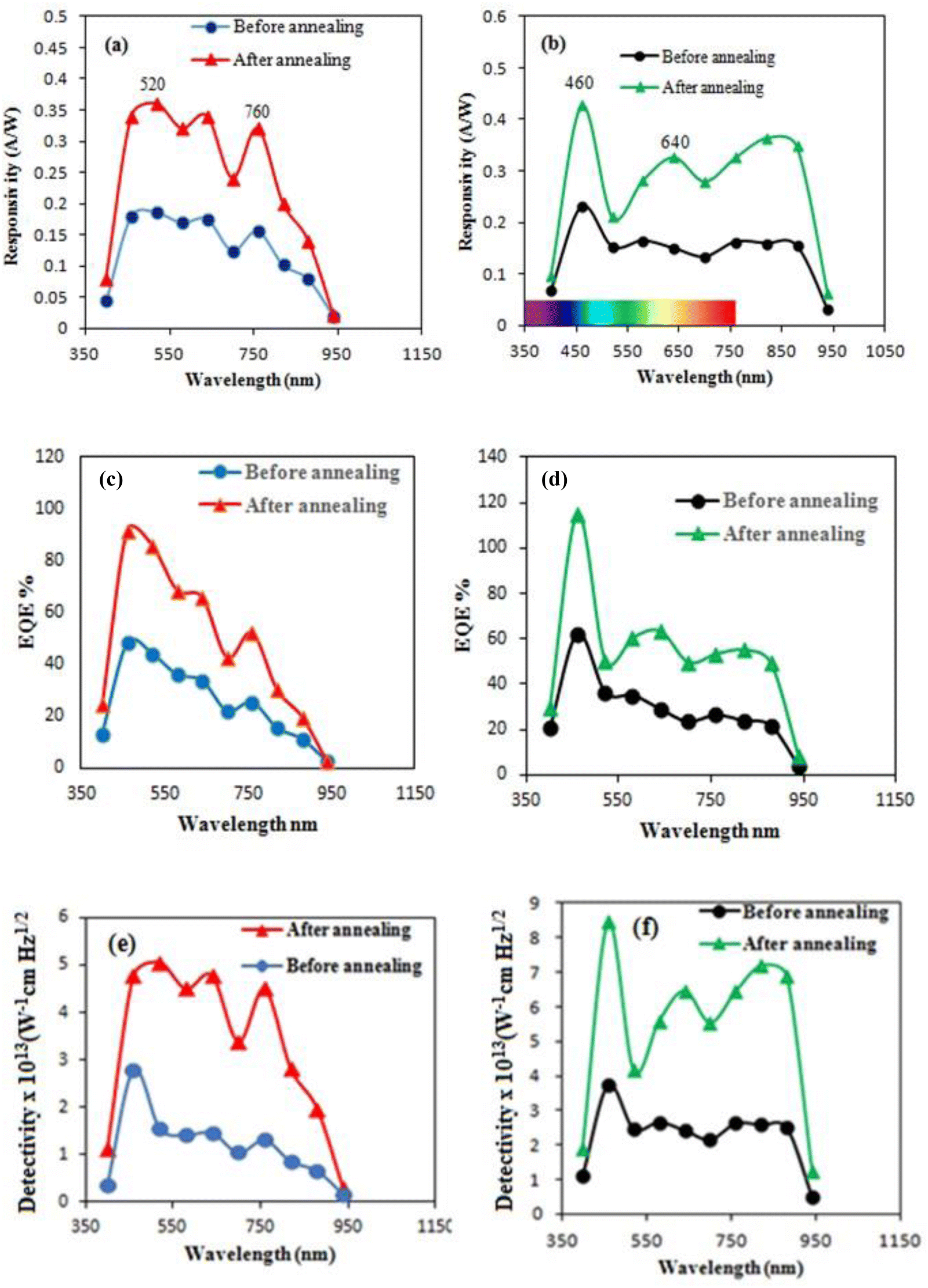
The built-in potential (Vbi) of the Au-decorated CdS/Si heterojunction before and after annealing was 1 and 2 V, respectively. Its value for Au-decorated CdS/Si is larger than the CdS/Si heterojunction; Fig. 8c. This is due to the presence of Au, which forms a Schottky contact with CdS. The work function of Au is 5.1 eV, and the electron affinity of CdS and Si is 0.2 eV and 4.05 eV, respectively. The barrier height rises as a result of band bending at the CdS surface. The presence of the Au shell adds a dipole layer that increases the potential drop across the junction. After annealing, the barrier height increased for both heterojunctions as a result of the decreased trap-assisted recombination, reduced lattice defects, and reduced carrier scattering.46,47 Fig. 9a shows the spectral responsivity (Rλ) of self-driven CdS/Si photodetector before and after annealing at zero bias. Rλ is the ratio of photocurrent to light power at a certain wavelength  . Two peaks of response were observed at 520 and 760 nm with responsivity of 0.19 and 0.16 A W−1 respectively before annealing. The first peak originated from the absorption edge of the CdS layer
  while the second peak is related to the absorption edge of the silicon substrate. After annealing, Rλ increased to 0.36 and 0.31 A W−1 at 520 and 760 nm, respectively, as shown in Fig. 9b. This is attributed to the increase of depletion layer width because of the capacitance decrease.40 The increase in CdS mobility (μ) was observed due to the longer diffusion length
  where τ is the minority carrier lifetime of the minority charge carriers.48,49 Fig. 9b: the effect of IPL annealing on the responsivity of a self-powered Au-decorated CdS/Si photodetector. Three peaks of response are seen at 460, 640, and 850 nm with responsivity of 0.42, 0.32, and 0.37 A W−1, respectively. The exciton formation in CdS, which is boosted by the plasmonic effect of Au shell nanoparticles, may be connected to the first peak. The second peak is due to band-to-band transition in CdS, and this peak was improved by the presence of Au nanoparticles and the plasmonic-induced local field enhancement. The light absorbed by the silicon substrate is responsible for the third response peak.33,49,50 After annealing, the responsivity increases remarkably due to the increase in the depletion region width. Fig. 9c & d show the external quantum efficiency (EQE) as a function of wavelength for CdS/Si and Au-decorated CdS/Si heterojunctions.
 | ||
| Fig. 9 (a) Responsivity of self-driven CdS/Si photodetector before and after annealing, (b) responsivity plot of Au-decorated CdS/Si photodetector, (c) EQE of CdS/Si photodetector, (d) EQE of Au-decorated CdS/Si (e) detectivity of CdS/Si photodetector, and (f) detectivity of Au-decorated CdS/Si heterojunction after annealing. | ||
The EQE increased significantly from 47% to 90% at 460 nm after IPL annealing, indicating an improved collection efficiency of the photo-generated carriers. This improvement is attributed to the reduction of surface states and grain boundaries of CdS nanoparticles, which play an active role in the recombination of photo-generated carriers. Contrarily, the EQE of the Au-decorated CdS/Si photodetector exceeded unity after annealing due to the formation of LPR, which originated from the presence of Au nanoparticles that enhanced light absorption at 500 nm.37,51–53 The specific detectivity plots of self-driven CdS/Si and Au-decorated CdS/Si photodetectors before and after annealing are shown in Fig. 9e & f. The detectivity of the Au-decorated CdS/Si photodetector was higher than the CdS/Si photodetector after annealing due to the higher responsivity, surface state reduction, grain boundaries, and small surface leakage.54–58 Table 4 shows a comparison of the figures of merit of the fabricated photodetectors after IPL annealing with some reported CdS and CdTe@CdS core–shell-based silicon heterojunctions.
| Parameter | CdTe@CdS/Si59 | CdS/Si60 | This work (IPL-annealed CdS/Si & Au-decorated CdS/Si) | Improvement demonstrated |
|---|---|---|---|---|
| Responsivity (A W−1) | 0.901 (810 nm) | 0.0648 (broadband) | 0.36 at 520 nm | 2× higher than CdS/Si,60 comparable to CdTe@CdS59 but with simpler processing |
| 0.42 at 460 nm | ||||
| Detectivity (Jones) | 4.5 × 10¹¹ | 1.31 × 10¹⁰ | Expected improvement (defect reduction) | Higher than CdS/Si60 and close to CdTe@CdS/Si59 with better crystallinity |
| EQE (%) | 1.1 × 10² | 3450.5 (pyro effect) | Likely enhanced (defect passivation) | More stable/reproducible than pyro-effect-dependent EQE |
| Spectral range | Visible-NIR (810 nm peak) | Visible-NIR (up to 1550 nm) | Visible-NIR (520–760 nm demonstrated) | Tunable performance via IPL, not limited by pyro effects |
| Processing method | Two-step laser ablation | Hydrothermal + Si planar | Laser ablation + IPL annealing | Rapid (IPL), scalable, and defect-passivating |
| Key advancement | Core–shell complexity | Pyro-phototronic effect | Crystallinity improvement & depletion layer control | Simpler than core–shell, more stable than pyro-effect devices |
Fig. 10a & b shows the photographs of freshly prepared and stored CdS and Au-decorated CdS colloids. The color of the CdS colloid was light yellow, while the Au-decorated CdS colloid was dark yellow. No significant change in the color of the colloids was observed after storing them in the lab for five months, confirming the stability of these products. Actually, the agglomeration of the nanoparticles and degradation of the product may result in remarkable change in the color of the colloids. As shown in Fig. 10c, the responsivity of the CdS/Si and Au-decorated CdS/Si photodetectors is slightly decreased after storage for five months, and the Au-decorated Si photodetector exhibits better stability than that of CdS/Si due to the presence of protective Au.
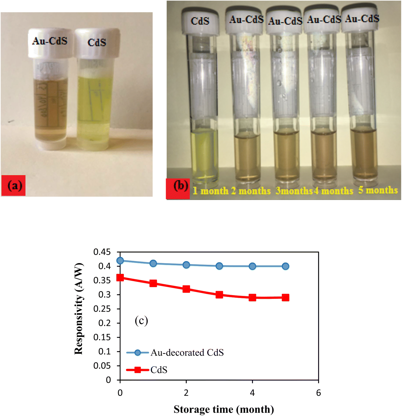 | ||
| Fig. 10 (a) Photograph of freshly prepared CdS and Au-decorated CdS colloids (b) photograph of colloids after five months of storage in the lab, and (c) variation of responsivity of CdS/Si and Au-decorated CdS/Si photodetectors with storage time. | ||
4. Conclusion
Using intense pulsed light (IPL) for post-irradiation treatment in the preparation of CdS and Au-decorated CdS nanoparticles has led to notable improvements in nanoparticle characteristics. IPL-induced photothermal effects caused localized heating, which altered surface charge, caused dissolution, and promoted aggregation. Au nanoparticle aggregation, surface alterations, and changes in electrical properties were the outcomes of post-IPL exposure, which also showed efficacy in changing the properties of nanomaterials. The increased built-in potential, following the IPL irradiation, has enhanced the electric properties of CdS and Au-decorated CdS. It indicates a promising approach to improve nanomaterial performance. Self-powered CdS/Si and Au-decorated CdS/Si photodetectors were fabricated. The figure of merit of the Au-decorated CdS/Si photodetector was enhanced significantly after IPL annealing. The responsivity of the Au-decorated CdS/Si photodetector at zero bias increased from 0.23 to 0.42 A W−1 at 460 nm after annealing. The effect of aging time on the performance of the photodetectors was studied.The present findings are in good agreement with the context of the published work related to the work under study. To the best of our knowledge, this is the first study where rapid thermal annealing is achieved by intense light pulses. The results obtained are backed by the theories that govern this work and highlight the IPL potential as a novel method for boosting the Au-decorated CdS nano-colloid's characteristics and paving the way for applications in optoelectronics, catalysis, and sensing.
Data availability
The datasets generated during and/or analyzed during the current study are available from the corresponding author (R. A. Ismail) on reasonable request Raid A. Ismail.Conflicts of interest
The authors declare that they have no known competing financial interests or personal relationships that could have appeared to influence the work reported in this paper.References
- A. Ghasempour, H. Dehghan, M. Ataee, B. Chen, Z. Zhao, M. Sedighi, X. Guo and M.-A. Shahbazi, Cadmium sulfide nanoparticles: preparation, characterization, and biomedical applications, Molecules, 2023, 28, 3857, DOI:10.3390/molecules28093857.
- L. Jie, X. Gao, X. Cao, S. Wu, X. Long, Q. Ma and J. Su, A review of CdS photocatalytic nanomaterials: morphology, synthesis methods, and applications, Mater. Sci. Semicond. Process., 2024, 161, 108288, DOI:10.1016/j.mssp.2024.108288.
- V. Lahariya, M. Michalska-Domańska and J. Sanjay, Dhoble Synthesis, structural properties, and applications of cadmium sulfide quantum dots, in Cadmium Sulfide Quantum Dots, Elsevier, 2023, pp. 235–266, DOI:10.1016/b978-0-323-85278-4.00018-0.
- B.-G. An, H.-R. Kim, Y. W. Chang, J.-G. Park and J. C. Pyun, Photosensors based on cadmium sulfide (CdS) nanostructures: a review, J. Korean Ceram. Soc., 2021, 58, 631–644, DOI:10.1007/s43207-021-00141-5.
- C. V. Reddy and J. S. Shim, Synthesis and characterization of CdS nanoparticles using a chemical precipitation method, in Nanostructures and Nanomaterials, CRC Press, 2016, pp. 83–86, DOI:10.1201/B19934-18.
- S. T. Hunt and Y. Román-Leshkov, Principles and methods for the rational design of core–shell nanoparticle catalysts with ultralow noble metal loadings, Acc. Chem. Res., 2018, 51, 1054–1062, DOI:10.1021/acs.accounts.7b00510.
- C. F. Jones, L. Resina, F. C. Ferreira, P. S. Alberte and T. Esteves, Conductive core–shell nanoparticles: synthesis and applications, J. Phys. Chem. C, 2024, 128, 11083–11100, DOI:10.1021/acs.jpcc.4c02012.
- B. Mohanty and J. Nayak, One-step synthesis, characterization and optoelectronic properties of cadmium sulfide nanocrystal, AIP Conf. Proc., 2020, 2220, 020076, DOI:10.1063/5.0002011.
- R. A. Ismail, W. K. Hamoudi and H. F. Abbas, New route for cadmium sulfide nanowires synthesis via pulsed laser ablation of cadmium in thiourea solution, Mater. Res. Express, 2018, 5, 025017, DOI:10.1088/2053-1591/aaaad5.
- Y. Cao, H. Yin, T. Fan, X. Liu and S.-M. Chen, Morphology-dependent of nanosizes CdS toward efficient photocatalytic Cr(VI) reduction, J. Nanopart. Res., 2020, 22, 232, DOI:10.1007/s11051-020-04926-3.
- J. Zhang, F. Jiang and L. Zhang, Fabrication of single-crystalline semiconductor CdS nanobelts by vapor transport, J. Phys. Chem. B, 2004, 108, 7002–7005, DOI:10.1021/jp036945v.
- J. Mo, Z. Feng, J. Hou, Z. Jia and X. Lv, Synthesis and photoluminescence properties of CdS hollow nanospheres by chemical vapor deposition, Optoelectron. Lett., 2011, 7, 161–163 CrossRef.
- Y. Li, Y. Hu, S. Peng, G. Lu and S. Li, Synthesis of CdS nanorods by an ethylenediamine assisted hydrothermal method for photocatalytic hydrogen evolution, J. Phys. Chem. C, 2009, 113, 9352–9358 CrossRef CAS.
- Z. Lei, J. Li, Y. Ke, Y. Zhang, H. Wang and G. He, Fabrication of macroporous cadmium sulfide with three-dimensional structure by solvothermal synthesis, J. Mater. Chem., 2001, 11, 1778–1780 RSC.
- F. H. Alkallas, S. M. Alghamdi, A. N. Al-Ahmadi, A. B. G. Trabelsi, E. A. Mwafy, W. B. Elsharkawy and R. A. Rezk, et al.. Photodetection properties of CdS/Si heterojunction prepared by pulsed laser ablation in DMSO solution for optoelectronic application, Micromachines, 2023, 14(8), 1546 CrossRef ..
- S. Das, A. Tripathi, A. Parida, D. Alagarasan and R. Naik, Visible light photodetectors based on hydrothermally synthesized Cd-Se-Te nanostructures, ACS Appl. Electron. Mater., 2024, 6(9), 6522–6533 CrossRef CAS ..
- A. Dutta, A. Medda, S. Ghosh, S. Sain and A. Patra, 2D CdSe/CdS core–shell nanoplatelets for high-performance photodetectors, ACS Appl. Nano Mater., 2022, 5, 8558–8565 Search PubMed.
- D. Li, Z. Chen, X. Wang, Z. Zhong, C. Chen and M. Wu, Synthesis of durian-like TiO2@CdS core–shell structure and study on H2 generation properties, Catalysts, 2022, 12, 1211 CrossRef CAS.
- S. S. Kanmani, M. Sarkaraikani and K. Ramachandran, Core/shell type ZnO/CdS nanocomposites: synthesis, characterization, and application for solar energy conversion, Adv. Sci. Lett., 2012, 5, 1–7 CrossRef.
- T. A. Welsch and M. F. Doty, PbS/CdS core/shell quantum dots designed to enable efficient photon upconversion for solar energy applications, ACS Appl. Opt. Mater., 2024, 2, 4080–4087 Search PubMed.
- C. J. Moon, J. W. Park and Y. R. Jang, et al., Intense pulsed light annealing of solution-based indium–gallium–zinc–oxide semiconductors with printed Ag source and drain electrodes for bottom gate thin film transistors, Sci. Rep., 2024, 14, 1566 CrossRef CAS.
- G. García Guillen, V. A. Zuñiga Ibarra, M. I. Mendivil Palma, B. Krishnan, D. Avellaneda Avellaneda and S. Shaji, Effects of liquid medium and ablation wavelength on the properties of cadmium sulfide nanoparticles formed by pulsed-laser ablation, ChemPhysChem, 2017, 18, 1035–1046 CrossRef.
- X. Yang, B. Wang and Y. Mu, et al., Photocatalytic performance of cubic and hexagonal phase CdS synthesized via different Cd sources, J. Electron. Mater., 2019, 48, 2895–2901 CrossRef CAS.
- P. K. Mahato, S. Chaudhuri, S. Patel and P. Patra, Investigating the impact of annealing temperature on CdS nanoparticles: optimizing solar photovoltaic efficiency, IOP Conf. Ser. Earth Environ. Sci., 2024, 1375, 012016, DOI:10.1088/1755-1315/1375/1/012016.
- R. Sami and A. J. Ghazai, Preparation and characterization of structural and optical properties of CdS thin film spin coating prepared, J. Phys.: Conf. Ser., 2021, 1999, 012070, DOI:10.1088/1742-6596/1999/1/012070.
- R. A. Ismail, W. K. Hamoudi and H. F. Abbas, Synthesis of Au nanoparticles–decorated CdS nanowires via laser ablation in liquid for optoelectronic applications, Appl. Phys. A, 2018, 124, 683, DOI:10.1007/s00339-018-2110-7.
- L. Wang, Z. Liu and J. Han, et al., Stepwise synthesis of Au@CdS–CdS nanoflowers and their enhanced photocatalytic properties, Nanoscale Res. Lett., 2019, 14, 148, DOI:10.1186/s11671-019-2977-z.
- S. Srikanth, The effect of luminescence on crystalline CdS thin films prepared by chemical bath route, Int. J. Res. Appl. Sci. Eng. Technol., 2018, 6, 4558–4561, DOI:10.22214/ijraset.2018.4747.
- C. Wang, W.-Z. Yang, Z.-M. Feng, Z.-J. Cheng, Z. Jiang and C. Zhan, Selective passivation of surface toward bright yellow defective emission of CdS quantum dots, Inorg. Chem., 2023, 62(41), 16913–16918, DOI:10.1021/acs.inorgchem.3c02600.
- A. Sabah, S. Siddiqi and S. Ali, Fabrication and characterization of CdS nanoparticles annealed by using different radiations, Int. J. Chem. Biomol. Eng., 2010, 4, 532–539 Search PubMed.
- S. Aksay, XRD, optical and vibrational properties of annealed cadmium sulfide films, Estu Sci.– Se, 2018, 19, 1013–1022, DOI:10.18038/aubtda.425869.
- M. Kamalian, E. Hasani, L. Babazadeh Habashi and M. Gholizadeh Arashti, Impact of post-deposition annealing on the optical, electrical, and structural properties of CdS thin films for solar cell applications, Phys. B, 2024, 674, 415524, DOI:10.1016/j.physb.2023.415524.
- W. Belaid, S. Y. Gezgin, M. A. Basyooni-Kabatas, Y. R. Eker and H. Ş. Kiliç, Utilizing gold nanoparticle decoration for enhanced UV photodetection in CdS thin films fabricated by pulsed laser deposition: exploiting plasmon-induced effects, Nanomaterials, 2024, 14(5), 416, DOI:10.3390/nano14050416.
- E. A. Slejko, L. Cozzarini and V. Lughi, Engineering of colloidal nanocrystal thin films and their optoelectronic properties: A simple and effective route, Nano-Struct. Nano-Objects, 2020, 22, 100432 CrossRef CAS.
- L. Wang, Z. Liu, J. Han, R. Li and M. Huang, Stepwise synthesis of Au@ CdS-CdS nanoflowers and their enhanced photocatalytic properties, Nanoscale Res. Lett., 2019, 14, 1–9 CrossRef.
- R. Matin, M. S. Bashar, M. Sultana, A. N. Ahmed and A. Gafur, Annealing Effects on the Structural, Optical and Electrical Properties of Chemically Deposited CdS Thin Films using NH4Cl Complexing Agent, Int. J. Nanoelectron. Mater., 2018, 11(2), 221–232 Search PubMed.
- S. Pathak, S. Chaudhary, M. Shrivastav, N. Kumar, S. Varshney, M. Kumar, S. Sharma, F. Guzman, S. Kumar and C. Kumar, The effects of air-annealing on the performance of optical-electrical assessment of sputtered CdS film towards the Ag/n-CdS/p-Si(100)/Al photodetectors, Opt. Mater., 2024, 150, 115117, DOI:10.1016/j.optmat.2024.115117.
- H. H. Ahmed, Fabrication and study characteristics of CdS/Si heterojunction detector by CBD technique, Tikrit J. Pure Sci., 2012, 17, 169–175 Search PubMed.
- A. Manilal, S. Nair and L. R. Thoutam, Thermally induced enhancement of photoresponse in radio frequency-sputtered CdS thin-film photodetectors, Adv. Eng. Mater., 2024, 26(24), 2401942, DOI:10.1002/adem.202401942.
- Y. Al-Douri, M. Ameri, A. Bouhemadou and R. Khenata, Annealing temperature effect on structural, optical, morphological and electrical properties of CdS/Si(100) nanostructures, Microsyst. Technol., 2016, 22, 2529–2541, DOI:10.1007/s00542-015-2584-6.
- F. Salamon, Effect some factors on the structural properties of the CdS thin films prepared by chemical bath deposition, Int. Lett. Chem. Phys. Astron., 2016, 64, 1–10, DOI:10.18052/www.scipress.com/ilcpa.64.1.
- I. B. Sapaev, B. Sapaev, S. Sadullaev, J. S. Abdullayev, A. V. Umarov, R. U. Siddikov, A. A. Mamasoliev and K. S. Daliev, Influence of the parameters to transition capacitance at n-CdS-p-Si heterostructure, E3S Web Conf., 2023, 413, 04008, DOI:10.1051/e3sconf/202341304008.
- V. Bilgin, E. Sarica, B. Demirselcuk and K. Erturk, Characterization of CdS films and CdS/Si heterojunctions prepared by ultrasonic spray pyrolysis and their response to light, Phys. B: Condens. Matter, 2020, 599, 412499, DOI:10.1016/j.physb.2020.412499.
- S. Wang, Z. Shen, Y. Sun, H. Li, K. Zhang, L. Wu, J. Ao and Y. Zhang, Defects and surface electrical property transformation induced by elemental interdiffusion at the p–n heterojunction via high-temperature annealing, ACS Appl. Mater. Interfaces, 2021, 13, 12211–12220, DOI:10.1021/acsami.1c00096.
- B. Zhang, W. Wang, T. Sun and J. Wang, Nanostructured gold interlayer-enhanced self-powered photodetectors for visible and long-wave infrared dual-band applications, Laser Photon. Rev., 2005, 19(5) DOI:10.1002/lpor.202401329.
- Y.-J. Noh, G. Kim, H. Lee, J. Shin, K. An, M. Kumar and D. Lee, A review on intense pulsed light process as post-treatment for metal oxide thin films and nanostructures for device application, Nanotechnology, 2022, 33, 272001, DOI:10.1088/1361-6528/ac6314.
- H. J. Kim, C. J. Han, B.-W. Yoo, J. Lee, K. Lee, K. H. Lee and M. S. Oh, Effects of intense pulsed light (IPL) rapid annealing and back-channel passivation on solution-processed In–Ga–Zn–O thin film transistors array, Micromachines, 2020, 11, 508, DOI:10.3390/mi11050508.
- S. N. Moger, P. Kumar, G. K. Rao and M. M. G. Mahesha, Annealing assisted enhancement in photo response of PV deposited CdS thin films, Opt. Laser Technol., 2022, 149, 107868, DOI:10.1016/j.optlastec.2022.107868.
- P. M. Perillo and D. F. Rodriguez, Influence of low-temperature annealing time on CdS thin films, Phys. B, 2024, 680, 415828, DOI:10.1016/j.physb.2024.415828.
- A. J. Addie, R. A. Ismail and M. A. Mohammed, Amorphous carbon nitride dual-function anti-reflection coating for crystalline silicon solar cells, Sci. Rep., 2022, 12, 9902 CrossRef CAS.
- S. S. Shaker, R. A. Ismail and D. S. Ahmed, High-responsivity heterojunction photodetector based on Bi2O3-decorated MWCNTs nanostructure grown on silicon via laser ablation in liquid, J. Inorg. Organomet. Polym. Mater., 2022, 32, 1381–1388 CrossRef CAS.
- S. Supriya, S. Das, A. Parida and R. Naik, Cu-doped CdTe nanoparticles synthesized by colloidal approach for optoelectronic and photodetector application, Mater. Res. Bull., 2025, 189, 113486 CrossRef CAS.
- D. Alagarasan, S. Varadharajaperumal, K. D. A. Kumar, R. Naik, A. Arunkumar, R. Ganesan and E. E. S. Massoud, Optimization of different temperature annealed nanostructured CdSe thin film for photodetector applications, Opt. Mater., 2021, 122, 111706 CrossRef CAS.
- R. A. Ismail, E. T. Salim and H. T. Halbos, Preparation of Nb2O5 nanoflakes by hydrothermal route for photodetection applications: the role of deposition time, Optik, 2021, 245, 167778 CrossRef CAS.
- R. A. Ismail, W. K. Hamoudi and K. K. Saleh, Effect of rapid thermal annealing on the characteristics of amorphous carbon/n-type crystalline silicon heterojunction solar cells, Mater. Sci. Semicond. Process., 2014, 21, 194–199 CrossRef CAS.
- S. T. Kassim, H. A. Hadi and R. A. Ismail, Fabrication and characterization of high photosensitivity CuS/porous silicon heterojunction photodetector, Optik, 2020, 221, 165339 CrossRef CAS.
- S. S. Shaker, R. A. Ismail and D. S. Ahmed, Preparation of bismuth oxide nanoplatelets/Si photodetector by laser ablation in liquid under effect of an external magnetic field, Silicon, 2022, 14, 107–113, DOI:10.1007/s12633-020-00789-4.
- R. K. Abdulnabi, R. A. Ismail, M. H. Mohsin, M. F. Jawad, E. T. Salim and M. A. Fakhri, High-performance n-V2O5/p-Si heterojunction photodetector prepared by pulsed laser deposition: role of laser fluence, J. Mater. Sci.: Mater. Electron., 2025, 36(7), 426 CrossRef CAS )..
- Y. K. Abdalaah, O. A. Mahmood and S. S. Shaker, et al., Preparation of a nanostructured CdTe@CdS core–shell/Si photodetector by two-step laser ablation in liquid, J. Opt., 2024 DOI:10.1007/s12596-024-01720-5.
- Z. Ren, Q. Wang, G. Zhang, T. Zhang, J. Liu, S. Wang and S. Qiao, Self-powered CdS nanorods/planar-Si photodetector and its performance optimization by fully developing pyro-phototronic effect, Surf. Interfaces, 2023, 42, 103495 CrossRef CAS.
| This journal is © The Royal Society of Chemistry 2025 |