
 Open Access Article
 This Open Access Article is licensed under a
 Creative Commons Attribution 3.0 Unported Licence
Solvent-mediated crystallization and defect passivation mechanisms in ambient-air MAPbI3 films: a combined experimental and simulation study
Ichrak Touhami*ab,
Ouidad Beldjeblic,
Selma Rabhi *d,
Yaacoub Ibrahim Bouderbalae,
Béchir Dridi Rezguia,
Tarak Hidouri*f,
Amal BaQaisg,
Shima Sadaf*h,
Mir Waqas Alami and
Mongi Bouaïchaa
*d,
Yaacoub Ibrahim Bouderbalae,
Béchir Dridi Rezguia,
Tarak Hidouri*f,
Amal BaQaisg,
Shima Sadaf*h,
Mir Waqas Alami and
Mongi Bouaïchaa
aUniversité de Tunis El Manar, Campus Universitaire Farhat Hached, B.P. No. 94, Rommana, 1068 Tunis, Tunisia. E-mail: ichrak.touhami@etudiant-fst.utm.tn
bLaboratoire de Photovoltaïque, Centre de Recherches et des Technologies de l'Energie, Technopôle de Borj-Cédria, B.P. No. 95, Hammam-Lif, 2050 Tunis, Tunisia
cLaboratoire de Chimie Appliquée et Génie Chimique, Université Mouloud Mammeri, B.P. No. 17 RP, 15000 Tizi-Ouzou, Algeria
dLaboratory of Innovative Environmental Preservation Techniques, Department of Chemistry, Constantine 1 University, 25000 Constantine, Algeria. E-mail: selma.rabhi@umc.edu.dz
eApplied Optics Laboratory, Institute of Optics and Precision Mechanics, University of Ferhat Abbas, 19000 Setif, Algeria
fDepartment of Mathematical, Physical and Computer Sciences, University of Parma, 43124 Parma, Italy. E-mail: tarek.hidouri@unipr.it
gDepartment of Chemistry, College of Science, Princess Nourah Bint Abdulrahman University, Riyadh 11671, Saudi Arabia
hDepartment of Electrical Engineering, College of Engineering King Faisal University, Al-Ahsa 31982, Saudi Arabia. E-mail: ssadaf@kfu.edu.sa
iDepartment of Physics, College of Science, King Faisal University, Ahsaa 31982, Saudi Arabia
First published on 3rd July 2025
Abstract
Understanding solvent-induced crystallization and defect dynamics in hybrid perovskites is crucial for stable and high-efficiency solar cells. Here, we investigate the influence of DMF![[thin space (1/6-em)]](https://www.rsc.org/images/entities/char_2009.gif) :DMSO solvent ratios on the nucleation, grain boundary passivation, and optoelectronic behaviors of MAPbI3 thin films prepared under ambient conditions. X-ray diffraction and photoluminescence analyses reveal that increasing DMSO content promotes PbI2 segregation, which passivates grain boundaries and modulates trap-assisted recombination. These structural and photophysical changes are correlated with carrier lifetimes using time-resolved photoluminescence measurements and the simulated device performance using SCAPS-1D. We find that a DMF:DMSO ratio of (6:4) enhances the interplay between crystalline order, the energy disorder (Urbach tail), and the charge transport. Our findings provide mechanistic insights into how solvent coordination controls defect landscapes and interface energetics in perovskite films, offering a framework for rational solvent design in ambient-stable photovoltaics.
:DMSO solvent ratios on the nucleation, grain boundary passivation, and optoelectronic behaviors of MAPbI3 thin films prepared under ambient conditions. X-ray diffraction and photoluminescence analyses reveal that increasing DMSO content promotes PbI2 segregation, which passivates grain boundaries and modulates trap-assisted recombination. These structural and photophysical changes are correlated with carrier lifetimes using time-resolved photoluminescence measurements and the simulated device performance using SCAPS-1D. We find that a DMF:DMSO ratio of (6:4) enhances the interplay between crystalline order, the energy disorder (Urbach tail), and the charge transport. Our findings provide mechanistic insights into how solvent coordination controls defect landscapes and interface energetics in perovskite films, offering a framework for rational solvent design in ambient-stable photovoltaics.
1. Introduction
Solar energy is a leading renewable resource, offering abundant, clean, and eco-friendly power.1 This limitation has spurred significant interest in the development of new materials and alternative strategies for clean energy generation. Among these, perovskite materials have attracted considerable attention due to their exceptional optoelectronic properties and unique ABX3 crystal structure, where A is a monovalent cation, which can be an organic cation such as methylammonium (MA+) or formamidinium (FA+), an inorganic cation like cesium (Cs+), or a mixture of two or more of these cations to improve the stability and performance of the perovskite material. B is a divalent metal cation (commonly lead (Pb2+) or tin (Sn2+), and X is a halide anion (such as iodide (I−), bromide (Br−), or chloride (Cl−)). This structure forms a three-dimensional lattice in which the B-site cation is octahedrally coordinated by six X-site anions, and the A-site cation fills the voids between the octahedra as presented in Fig. 1. The flexibility in tuning the A, B, and X components allows precise control over the material's electronic, optical, and structural properties.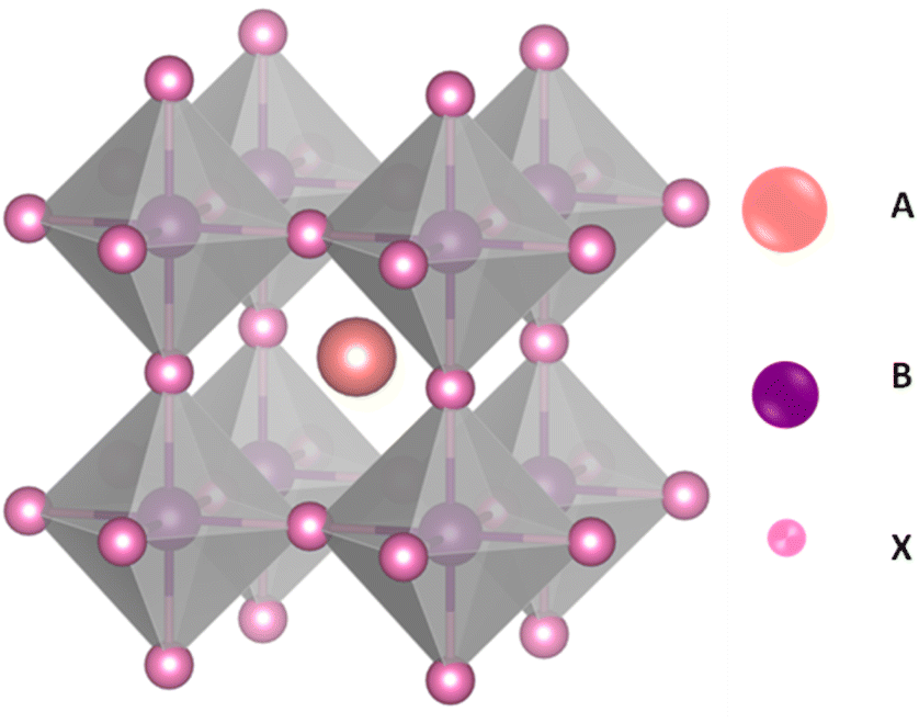 | ||
| Fig. 1 Perovskite crystalline structure realised by VESTA. | ||
Beyond their widely studied application in perovskite solar cells (PSCs), these materials also show great promise in a variety of other fields, including photocatalysis,2–4 light-emitting diodes (LEDs), lasers, and photodetectors,5,6 making them highly versatile candidates for next-generation energy and optoelectronic technologies. PSCs have quickly become a game-changing technology in the solar energy industry. A direct band gap, low exciton binding energy, excellent light absorption capabilities, and inexpensive manufacture are some of their many strong points.7 The potential of PSCs was first demonstrated in 2009 by Kojima et al.,8 who achieved a modest PCE of 3.8% using methyl ammonium lead iodide (MAPbI3) as the active layer. Since then, the field has advanced rapidly, with current efficiencies exceeding 26.7%,9 positioning PSCs as a leading candidate for next-generation PV technologies. However, their commercial viability remains hindered by intrinsic instability and defect mediated recombination. To address these challenges, researchers have increasingly focused on solvent engineering and defect passivation, particularly at the perovskite-hole transport layer (HTL) interface. Passivating defects at the perovskite/HTL (hole transport layer) interface by incorporating an excess PbI2 is considered as one of those approaches.10,11 This passivation reduces non-radiative recombination, thereby improving both efficiency and stability, as extensively reported in the literature. Here, dimethyl sulfoxide (DMSO) plays a pivotal role: its strong coordination with Pb2+ ions modulated solubility and crystallization kinetics, enabling the formation of uniform, large-grained perovskite films with tailored PbI2 distribution.12–15 Fabrication techniques also play a pivotal role in determining the quality and stability of PSCs. These techniques can generally be categorized into dry and wet processes, with the latter being more cost-effective and widely adopted in PSC manufacturing.16–19 Among wet processes, spin-coating is a frequently employed deposition method for fabricating MAPbI3 thin films. This method is implemented via two main approaches: the one-step and two-step deposition methods.20 The one-step method involves spin-coating a precursor solution containing CH3NH3I/MAI and PbI2, followed by annealing the films at temperatures alternating from 70 °C to 150 °C to crystallize the perovskite layer. This method is favored for its simplicity, cost-effectiveness, and suitability for large-scale production. In contrast, the two-step method involves initially spin-coating of a PbI2 film, followed by immersing it in a CH3NH3I solution to facilitate the formation of a MAPbI3 layer upon annealing. While this approach allows for greater control over film formation and facilitates the rapid fabrication of PSCs, it is often limited by the difficulty in controlling the fast crystallization of MAPbI3 throughout the procedure, particularly in ambient-air condition.21,22 To optimize PSC performance, analyzing the physical properties of MAPbI3 films is an essential process for achieving optimal device structures. Eventually, cooperation between solvent engineering, interface passivation and advanced fabrication protocols is key to fabricating high-potential perovskite solar cells. In this work, we combine experimental data of MAPbI3 including lifetime, bandgap, and thickness, with SCAPS-1D simulations to create an efficient protocol for accelerating the fabrication of perovskite solar cells. This approach not only saves time and resources but also provides a valuable framework for optimizing device performance. In plus, we propose the simulation of inverted perovskite solar cells, which have demonstrated higher stability compared to conventional perovskite solar cells. Although the power conversion efficiency of p-i-n structures remains lower than that of n-i-p devices, we suggest a new configuration incorporating novel hole transport layers, electron transport layers, and transparent conductive oxides to enhance photovoltaic performance.
2. Experimental and simulations details
2.1 Fabrication and characterization of MAPbI3 films
MAPbI3 films were spin-coated on glass substrates, via a one-step process, using four solutions with different DMF:DMSO ratios of 1:0, 8:2, 6:4 and 5:5. The samples obtained were named as S1, S2, S3 and S4, respectively for DMF:DMSO ratios of 1:0, 8:2, 6:4 and 5:5. Fig. 2 shows a schematic of the synthesis procedure of MAPbI3 highlighting the PbI2 segregation on it. Indeed, the solutions were prepared by dissolving 1 mol of methyl ammonium iodide (MAI) and 3 mol of lead iodide (PbI2) in 2 mL of a solvent mixture containing the mentioned ratios of DMF:DMSO. These solutions were stirred at 60 °C for 4 h to obtain homogeneous solutions. Then, they were spin-coated on the glass substrates with three successive rotation speeds: 500 rpm for 9 s, 1000 rpm for 30 s, and then 2500 rpm for 30 s. Finally, the four samples were annealed under ambient conditions at 110 °C for 15 min, to promote the crystallization of MAPbI3.
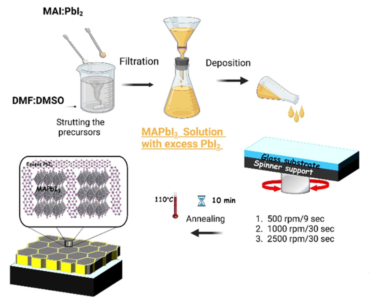 | ||
| Fig. 2 Overview schematics of MAPbI3 films fabrication procedures. | ||
The crystalline structure of the samples was identified by X-ray diffraction (XRD) using a Bruker D8 Advance diffractometer in Bragg–Brentano mode with CuKα radiation (λ = 1.54 Å). The transmittance and absorption spectra were collected using a monochromator-based PTS-2-QE/IPCE spectrophotometer. The room-temperature steady-state photoluminescence (PL) spectra were measured using a Jobin-Yvon HR 250 spectrophotometer using an excitation laser source of λ = 447 nm. The PL lifetime (TRPL) was measured by Edinburgh FLS980 spectrometer (Xe lamp/RCSPC) equipped with a Red PMT detector. The repetition rate is fixed at 4 MHz with a time range of 200 ns.
2.2 Simulation of perovskite solar cell
We proceed to analyze the MAPbI3-based PSC using the physical properties of MAPbI3 extracted experimentally and additional integration of theoretical/simulation approaches through the Solar Cell Capacitance Simulator SCAPS-1D version 3.3.10.23–27 The simulation was performed simultaneously based on a traditional drift-diffusion model and solving the electron and hole continuity eqn (1) and (2) as well as the Poisson's eqn (3).
 | (1) |
 | (2) |
 | (3) |
| TCO | 3D-PVK | HTLS | ETLs | ||||||
|---|---|---|---|---|---|---|---|---|---|
| a This study. | |||||||||
| Parameters | IZO | MAPbI3 | CBTS | Me-4PACz | PATAA | NiO | Se/Te:Cu2O | STO | MZO |
| Thickness (μm) | a | a | a | a | a | a | a | a | a |
| Eg (eV) | 3.5 | a | 1.9 | 3.3 | 2.95 | 3.8 | 1.88 | 3.2 | 3.35 |
| χ (eV) | 4.5 | 3.88 | 3.6 | 2.8 | 2.3 | 1.4 | 3.53 | 4 | 4 |
| ε | 10 | 24.1 | 5.4 | 10 | 3.5 | 10.7 | 7.11 | 8.7 | 66 |
| Cb (cm−3) | 1 × 10¹⁹ | 8.1 × 10¹⁸ | 2.2 × 10¹⁸ | 1 × 10¹⁹ | 2 × 10²¹ | 2 × 10¹⁹ | 2.02 × 10¹⁷ | 1.7 × 10¹⁹ | 1 × 10¹⁹ |
| Vb (cm−3) | 1 × 10¹⁹ | 8.1 × 10¹⁸ | 1.8 × 10¹⁹ | 1 × 10¹⁹ | 2 × 10²¹ | 1.8 × 10¹⁹ | 1.17 × 10¹⁹ | 2 × 10²⁰ | 1 × 10¹⁹ |
| μe (cm2 V−1 s−1) | 1 × 10⁻² | 1 | 30 | 6 | 1 × 10⁻⁴ | 12 | 1297 | 5.3 × 10³ | 0.05 |
| μn (cm2 V−1 s−1) | 1 × 10⁻³ | 1 | 10 | 24 | 1 × 10⁻⁴ | 28 | 1297 | 6.6 × 10² | 0.05 |
| Na (cm−3) | 1 × 10¹⁸ | 1 × 10¹⁴ | 0 | 0 | 0 | 0 | 0 | 2 × 10¹⁶ | 1 × 10¹⁷ |
| Nd (cm−3) | — | 1 × 10¹⁴ | 1.1 × 10¹⁵ | 1 × 10¹⁸ | 1.0 × 10¹⁸ | 5 × 10¹⁹ | 3.0 × 10¹⁸ | 0 | 0 |
| Nt (cm−3) | 1 × 10¹⁴ | a | 1.0 × 10¹⁴ | a | 1.0 × 10¹⁴ | 1 × 10¹⁴ | 1.0 × 10¹⁵ | 1 × 10¹⁴ | |
| Reference | 28 | 29 | 30 | 31 | 32 | 33 | 34 | 35 | |
3. Results and discussion
3.1 Structural and optical analysis
Fig. 2 displays the XRD pattern of MAPbI3 films prepared with different DMF:DMSO ratios, maintaining the same excess of PbI2 all the samples. A mixture of both the tetragonal phase of MAPbI3 and the hexagonal phase of PbI2 was observed for all films. The tetragonal phase of MAPbI3 can be verified by the existence of (110), (112), (211), (202), (220), (222), (312), (224), (330) and (404) planes.10,36 All the films display a polycrystalline nature with a preferred orientation along the (110) plane. However, the peaks at 12.60° and 37.83° are attributed to the (001) and the (003) crystal planes of the hexagonal structure of PbI2, confirming the presence of residual PbI2 excess in all samples. Because we use an excess solution to prepare the films, it is expected that PbI2 will appear as the dominant phase in comparison to the main perovskite phase. This residual PbI2 plays a beneficial role in forming a passivation layer that enhances the interface between the perovskite layer and the HTL, improving the charge transport and reducing recombination losses.11,37
On the other hand, Fig. 3 shows that there is no shift in peak positions related to the MAPbI3 tetragonal phase. This is reflecting the fact that DMF:DMSO ratios do not influence the lattice parameters (a and c lattice parameters). In contrast, with raising DMSO content up to 50%, a slight shift of the (001) plan related to the PbI2 hexagonal phase towards higher diffraction angles is observed. This result suggests a lattice contraction within the PbI2 structure by decreasing their lattice parameters (a and/or c lattice parameters). The (001) peak shift highlights the DMSO effective role in ambient-air processing since it coordinates with Pb2+ ions during crystallization. Indeed, it form an intermediate PbI2-DMSO complexes that delay the crystallization and allow for more ordered packing of PbI2 layers, resulting in a more stable perovskite film.
 | ||
| Fig. 3 X-ray diffraction spectra of perovskite layers for different DMF:DMSO ratios. | ||
The lattice parameters a and c of the MAPbI3 tetragonal phase of our samples were determined using Bragg's law (eqn (4) and (5)). The obtained values are displayed in Table 2.
|
2dsinθ = nλ
| (4) |
 | (5) |
:DMSO ratio, structural parameters, thicknesses, band gap energy (Eg), and disorder energy (Eu) of the prepared perovskite films
| Samples | S1 | S2 | S3 | S4 |
|---|---|---|---|---|
| DMF:DMSO ratio |
1:0 |
8:2 |
6:4 |
5:5 |
| Lattice parameters of MAPbI3 phase (Å) | a = 8.8688 | a = 8.8691 | a = 8.8679 | a = 8.8622 |
| b = 8.8688 | b = 8.8691 | b = 8.8679 | b = 8.8622 | |
| c = 11.3564 | c = 11.3548 | c = 11.3593 | c = 11.3553 | |
| (110)MAPbI3/(001)PbI2 | 0.51 | 0.3 | 0.32 | 0.14 |
| FWHM of (001)-PbI2 | 0.120 | 0.120 | 0.096 | 0.12 |
| FWHM of (110)-MAPbI3 | 0.072 | 0.072 | 0.096 | 0.072 |
| D (nm) of MAPbI3 | 104.67 | 99.7 | 94.8 | 86.6 |
| D (nm) of PbI2 | 61.33 | 68.51 | 72.19 | 82.80 |
| ε of MAPbI3 | 0.18 | 0.19 | 0.2 | 0.23 |
| Thicknesses (nm) | 810 | 820 | 813 | 800 |
| Eg (eV) | 1.48 | 1.43 | 1.46 | 1.50 |
| Eu (meV) | 154.5 | 288.5 | 206 | 115 |
| Lifetime average τavg (ns) | 768.52 | 741.83 | 845.9 | 765.3 |
From Table 2, the lattice parameters of MAPbI3 tetragonal phase of all the samples are around 8.87 Å and c = 11.35 Å, confirming that the DMF:DMSO ratios have no effect. It is reported that the range of the bulk values of a and c are from 8.83 Å to 8.90 Å, and from 12.60 Å to 12.68 Å, respectively.38 In comparison, our measured c value is lower than these later, meaning that the films are subject to a compressive stress formed during solvent evaporation and annealing treatment. Furthermore, by examining the intensity of peaks from Fig. 3, it can be observed that the intensity of all the XRD peaks increases for the (5:5) DMF:DMSO ratio suggesting an enhanced crystallinity. This improvement is attributed to more controlled crystallization dynamics where the presence of DMSO facilitates the formation of intermediate PbI2·DMSO complexes that slow down solvent evaporation and promote gradual nucleation.39 As a result, this sample exhibits smaller MAPbI3 crystallites (86.6 nm) and larger PbI2 grains (82.8 nm), as reported in Table 2. The growth of larger PbI2 crystallites is particularly beneficial, as it correlates with improved defect passivation at grain boundaries. This is supported by the decrease in the (110)MAPbI3/(001)PbI2 peak intensity ratio from 0.51 to 0.14 with increasing DMSO content (see Table 2), confirming the enhanced PbI2 crystallization.40 In contrast to mixed solvent systems, the film prepared using pure DMF (1:0) exhibits the largest MAPbI3 crystallite size (104.67 nm) and the smallest PbI2 crystallites (61.33 nm), indicating rapid and uncontrolled crystallization. This behavior results from the fast evaporation of DMF, which hinders the formation of intermediate phases that are essential for controlled nucleation and effective defect passivation. As the DMSO content increases, a gradual decrease in MAPbI3 crystallite size is observed from 104.7 nm to 86.6 nm accompanied by an increase in PbI2 grain size. This trend highlights the role of solvent coordination in modulating crystallization dynamics. Specifically, the formation of PbI2·DMSO complexes slows down the crystallization process, allowing for more uniform grain growth and improved film morphology.
Additionally, the strain (ε) in the perovskite lattice increases with DMSO content, from 0.18 in S1 to 0.23 in S4. This may be linked to the interfacial stress caused by larger PbI2 inclusions. These XRD-based observations confirm that while high DMSO content promotes crystallinity and passivation, it also introduces residual strain, highlighting the importance of tuning solvent composition.
For further explanation, the average (D) of crystallite sizes and the strain (ε) in films were calculated by the Scherrer and Williamson–Hall methods (eqn (6)) and (eqn (7)), from the XRD pattern.41 The values were recorded in Table 2.
 | (6) |
 | (7) |
The optical transmittance spectra of MAPbI3 films with different DMF:DMSO ratios, are shown in Fig. 4a. These spectra were used to calculate the film thicknesses by the envelope method.42 The envelope method is based on analyzing the interference fringes that appear in the optical transmittance spectra (Fig. 4a), which result from constructive and destructive interference of light within the film. These fringes arise from multiple reflections at the air/film and film/substrate (glass) interfaces. In our study, all MAPbI3 films exhibited clear oscillatory behavior, indicating sufficient film thickness and optical smoothness to allow interference effects. This technique enables the determination of both the wavelength-dependent refractive index n(λ) and the film thickness d without requiring cross-sectional scanning electron microscope (SEM) imaging. Therefore, it serves as a non-destructive and effective approach for characterizing thin films deposited on transparent substrates. Using the Swanepoel method and the eqn (8), the refractive index is determined by utilizing the transmittance envelope maxima (Tmax) and minima (Tmin).42
 | (8) |
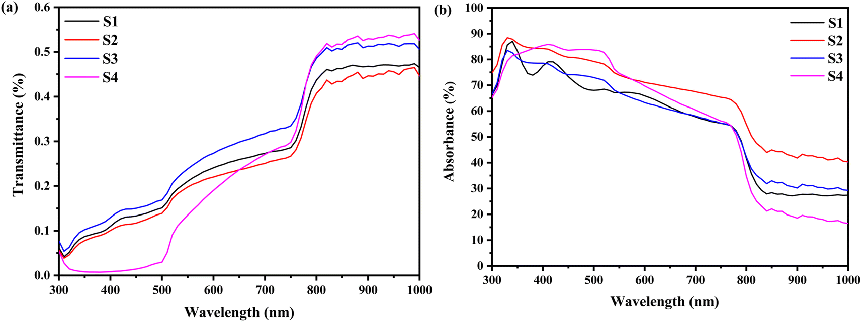 | ||
| Fig. 4 (a) Optical transmittance spectra, (b) absorbance spectra of MAPbI3 films with different DMF:DMSO ratios of samples S1, S2, S3 and S4. | ||
The factor s is the refractive index of the glass substrate (typically s ≈ 1.51). By applying the standard envelope method formula (eqn (9)), the film thickness (d) can be estimated without physical cross-sectioning.42
 | (9) |
This method is especially suitable for semi-transparent and uniform thin films deposited on transparent substrates. The calculated film thickness values obtained from this approach are reported in Table 2. Furthermore, in the visible range, the films displayed a low transmittance of less than 0.3%, due to their high absorbance. We also noted an absorption edge at around 750 nm, corresponding to the optical band gap of the MAPbI3 films.
Besides, the absorption spectra of MAPbI3 films are shown in Fig. 4b. All the samples exhibited a high absorbance covering a broad range of light from the ultra-violet to the near-infrared region. Samples S2 and S4 samples represent the higher absorbance values. These results suggest the strong light absorption of our perovskite films, which works as the solar cells' active layer, causes the higher short-circuit current density.
Furthermore, the absorption edge of the films slightly shifts to lower wavelengths as the DMSO content increases. It mainly arise from the nanoscale structural (in the present case, it is due to the reduction in the crystallite size of MAPbI3 film). This reflects an increase in the optical band gap (Eg). The Tauc formula (eqn (10)) is used to compute it:
| (αhν)2 = A(Eg − hν) | (10) |
 | (11) |
 | ||
| Fig. 5 (a) Tauc plots, (b) band gap energy and disorder energy. (c) PL spectra of S1, S2, S3 and S4. | ||
Both energy band gap and disorder energy (Urbach tail) are represented as a function of DMF:DMSO ratios in Table 2 and Fig. 5b. As can be seen, the variations of these two parameters have opposite trends. The variation in the optical band gap (Eg) of MAPbI3 films with different DMF:DMSO ratios is primarily attributed to changes in crystallite size and structural disorder. As the DMSO content increases from 0% to 20%, Eg decreases from 1.48 eV to 1.43 eV due to the formation of intermediate PbI2·DMSO complexes, which promote better crystallization and reduce energetic disorder.43 This is clear from the increased Urbach energy (Eu), indicating a higher density of localized states that narrows the apparent band gap.44 However, as the DMSO content increases further (up to the 5:5 ratio), Eg rises to 1.50 eV.45 This is associated with a reduction in crystallite size and a decrease in disorder (Eu = 115 meV), which suggests improved structural ordering and fewer sub-bandgap states. Additionally, the smaller grain size at higher DMSO content may introduce mild quantum confinement effects, contributing to the widening of the band gap. These results confirm that both crystallite size and energetic disorder, modulated by solvent ratio, play a critical role in tuning the band gap of MAPbI3 films processed under ambient conditions.
However, other samples possess higher disorder energy implying that this sample displays the most significant structural disorder, which is confirmed by its lowest XRD peak intensity. The elevated density of localized states within the band gap may stem from a significant concentration of lattice defects, grain boundaries, or impurities, resulting in enhanced optical absorption in the sub-bandgap region. The high absorbance from the ultra-violet to the near-IR region, with a band gap in the range of 1.43–1.50 eV of the MAPbI3 thin films, proves their potential as an effective absorber layer in solar cells.
Fig. 5c illustrates the PL spectra of MAPbI3 films prepared with varying DMF:DMSO ratios and deposited on glass substrates. All films display a characteristic red emission peak in the visible range attributed to the radiative recombination of the photogenerated carriers across the MAPbI3 bandgap. Specifically, the red band ‘maxima is located around 781.19 nm (1.58 eV), 782.12 nm (1.58 eV), 780.26 nm (1.59 eV), and 774.48 nm (1.60 eV) correspond to 1:0, 8:2, 6:4 and 5:5 DMF:DMSO ratios, respectively. These values align closely with the optical bandgap energies derived from UV-Vis measurements (Table 2), confirming the intrinsic electronic transitions between the valence band (VB) and the conduction band (CB) of MAPbI3.46–48 In addition, the narrow symmetric PL profiles further suggest better material quality with minimal defects and a well-crystallized perovskite film. Notably, the blueshift of the PL peak position with increasing DMSO content can be attributed to the formation of an intermediate adduct phase during crystallization, inducing lattice strain that slightly widens the bandgap. In plus, it could be assigned to the growth of PbI2 at the grain boundaries that itself perturb the perovskite's electronic structure. Furthermore, the reduction of crystallites size of MAPbI3 can introduce a quantum confinement effect that amplifies the bandgap could be another reason for the observed blueshift. As shown in Fig. 5c, the PL intensity increases when the DMSO content increases from 0 to 20%, peaking at the 8:3 DMF:DMSO ratio, then it decreases as a function of DMSO content, and reaches a minimum value for 5:5 DMF:DMSO ratio. The rise in the PL peak intensity with 20% DMSO indicates an improved crystal phase formation and increased electron–hole recombination pathways; as DMSO facilitates intermediate adduct phase formation during deposition, enabling uniform crystal growth with fewer defects. However, beyond 20% DMSO, the PL intensity decreases due to the reduction of the radiative recombination rate of MAPbI3 films. The excessive DMSO in sample S4 destabilizes the adduct decomposition during annealing by extending solvent retention leading to an incomplete perovskite conversion, an amorphous PbI2 aggregation, or disordered MAPbI3 growth. In addition, the residual DMSO solvent can lead to the creation of halide vacancies or charge traps by acting as a Lewis base. The decline coincides with excess DMSO and lead diiodide, as confirmed by XRD analysis. Therefore, while the excessive PbI2 treatment was found to passivate grain boundaries, and suppress the formation of trap states in the perovskite material, enhancing charge carrier movement and decreasing electron–hole recombination rate,49 its overuse introduces new defects that counteract its benefits.
The latter improves carrier dynamics and the overall optoelectronic performance of the MAPbI3 films by facilitating more efficient charge carrier extraction and transport, which is critical for applications in photovoltaic and optoelectronic devices. The PL analysis is in good agreement with XRD and optical (UV-Vis) data.
In the photovoltaic field, solar cells operate following three processes: charge carrier generation, separation and then collection. Among these, maximizing charge collection is one of the overarching goals of these cells. To elucidate the interplay between material properties and carriers, we conducted time resolved photoluminescence (TRPL) measurement. This technique quantifies carrier lifetimes, offering insights into recombination kinetic and defect-mediated losses.
Fig. 6 presents the TRPL decay measurements of samples S1, S2, S3 and S4, showing a multi-exponential decay profile. The bi-exponential function (eqn (12)) is used to fit the TRPL decay comprising fast and slow components which correspond to defect-mediated non-radiative recombination at trap states and radiative band-to-band recombination, respectively.
 | (12) |
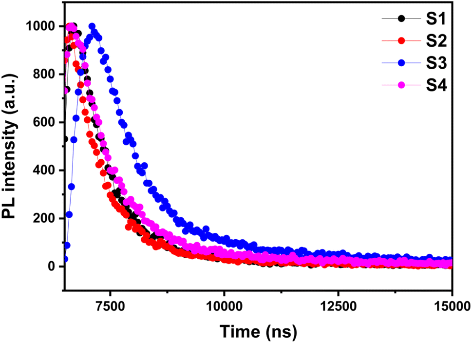 | ||
| Fig. 6 TRPL spectra of MAPbI3 films prepared with different DMF:DMSO ratios (S1, S2, S3 and S4). | ||
The average carrier lifetime derivates from TRPL decay measurements are presented in Table 2. The sample S3 exhibits the longest decay lifetime (τ = 845.9 ns) indicative of minimal non-radiative recombination. As confirmed by XRD and earlier optical analysis, this extended carrier lifetime results from efficient defect passivation at grain boundaries, where residual PbI2 compensates for iodide vacancies and under-coordinated Pb2+ defects. In contrast, S2 and S4 exhibit shorter PL lifetimes, indicative of recombination dominated by defects. A low amount of DMSO (sample S2) is insufficient to passivate defects leading to an increase in the trap density. On the other hand, an excessive amount (sample S4) induces the formation of amorphous PbI2 and unreacted DMSO residues which form deep-level traps. Therefore, an optimized intermediate DMF:DMSO ratio (6:4) provides the best balance between film uniformity, crystallinity, passivation, and charge transport properties, as supported by XRD, PL, and TRPL. These results underscore the delicate balance required in solvent engineering.
3.2 Modulization and simulation
In this work, the experimentally obtained parameters (τavg, thickness, and bandgap) of samples S1–S4 were implemented in SCAPS-1D simulations to model the performance of RGO/Me-4PACz/MAPbI3/LiF-C60-SnO2/IZO-structured PSCs. In the proposed structure, RGO was employed to enhance thermal stability, maintain PSC performance under high-temperature conditions, and improve device flexibility. On the other hand, IZO serves as an efficient back contact owing to its excellent optical transparency and electrical properties. Fig. 7 presents the impact of varying DMF:DMSO ratios (1:0, 8:2, 6:4, and 5:5) on the performance of perovskite solar cells under front and rear illumination, with all samples exhibiting the same excess of PbI2. For the sample S1 (1:0) and S3 (6:4), almost the same photovoltaic parameter are observed due to the poor film quality arising from the rapid evaporation because of presence of high ratio of DMF. Consequently, this last is evaporated rapidly leading to poor crystallization in the film. However, the sample S2 (8:2) improves the crystallization with the addition of DMSO, enhancing front illumination performance due to the better absorption and reduced defects. Interestingly, S4 (5:5) shows a reduced PL intensity reflecting a lower electron–hole recombination rate in the MAPbI3 films. Despite this improvement, slower crystallization may lead to residual defects that affect overall performance under rear illumination, although front illumination remains reasonable. These results indicate that front illumination is sensitive to perovskite film quality, while rear illumination highlights back contact passivation and light management. In conclusion, S3 achieves the most balanced performance and S4 shows promising reduction in recombination losses. In the next section, we will explore optimization strategies to enhance photovoltaic performance by selecting the appropriate HTL and ETL with optimal thickness, Eg, defect density (Nt), and parasitic resistances. The structural and optical results of MAPbI3 films prepared with different DMF:DMSO ratios, passivated the interface with PbI2 excess, proved that almost all these samples are suitable as absorbing layers in PCS, among them, S3 shows the best PV performance. In the next section, we will utilize S3 to find the optimal parameters by testing other ETLs, HTLs and TCO (back contact) to enhance PV performances.
 | ||
| Fig. 7 (a) J–V curves, for all samples. Inset showing a table summarizing the PV parameters. (b) The band diagram of one of the samples. | ||
In this subsection, the performance was analyzed using new HTL like CBTS, NiO, and Se/Te:CuO2, with ETL like SnS2, MZO, and STO (see Fig. 8). These carriers transporting layers result in the improvement of all PV performances where the PCE improved from 25.11% to 25.47%, VOC from 1.067 V to 1.071 V, JSC improved from 28.76 to 28.78 mA cm−2, and FF improved from 81.80% to 82.61%. These performances can be further optimized by investigating the effects of the thickness and defect density of the perovskite layer, which has the most significant impact on device performance.
 | ||
| Fig. 8 Histogram with PV performances of different configurations of PSCs. | ||
The results depicted in Fig. 9 demonstrate a strong dependence of PV performance on both the thickness and defect density (Nt) of PVK absorber layer. Specifically, increasing the PVK thickness from sub-micron levels up to 1 μm leads to notable improvements in PCE, VOC, JSC, and FF. This enhancement can be attributed to the improved light absorption and increased generation of photocarriers within the thicker absorber layer, which allows for more efficient photon harvesting across the solar spectrum.50 In contrast, increasing the defect density within the PVK layer has a detrimental effect on device performance. Higher values of Nt introduce more non-radiative recombination centers, which reduce carrier lifetime and increase recombination losses.51 These findings highlight the critical role of material quality in perovskite solar cells, emphasizing the need for optimized fabrication processes that minimize intrinsic and interfacial defect densities. The optimal performance is achieved at a PVK thickness of 1 μm and a defect density of 1 × 1013 cm−3, representing an ideal balance between efficient light absorption and reduced recombination losses. At these conditions, the device exhibits a PCE of 28.7%, VOC of 1.216 V, JSC of 29.30 mA cm−2, and FF of approximately 89%. Interestingly, variations in the thickness and defect density of the HTL, ETL, and TCO layers exhibit minimal influence on the overall photovoltaic performance.52 This indicates that once these layers fulfill their roles in charge transport and optical transparency, further optimization yields minimal gains. In contrast, the perovskite absorber layer has a dominant influence, as it directly governs light absorption and carrier generation.
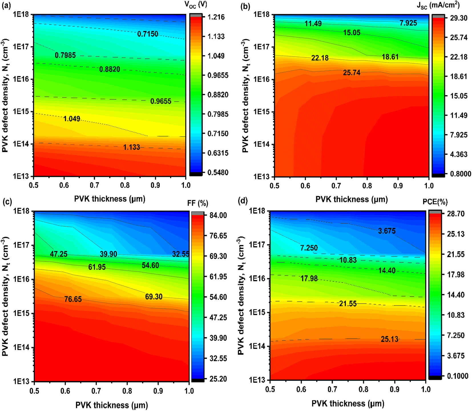 | ||
| Fig. 9 Contour plots of the effect of thickness and defect density (Nt) of PVK layer on the PV performances. | ||
The performance of the perovskite solar cell significantly declines as temperature increases from 275 K to 450 K, as illustrated in the Fig. 10. This reduction in PCE is primarily due to the thermally activated increase in non-radiative recombination, which lowers VOC and FF. Therefore, ensuring thermal stability through material engineering and proper device encapsulation is essential for maintaining high performance in real-world operating conditions.
 | ||
| Fig. 10 Influence of the temperature on the PCE of PSC. | ||
After applying the optimized MAPbI3 thickness and defect density, all photovoltaic parameters improved notably. The PCE increased from 25.47% to 28.70%, VOC from 1.071 V to 1.182 V, JSC from 28.78 to 29.25 mA cm−2, and FF from 82.61% to 82.97% (see Fig. 11(a)). These enhancements are mainly due to improved light absorption and reduced recombination losses. The optimal thickness ensures efficient photon harvesting, while the lower defect density suppresses non-radiative recombination, leading to better carrier collection and overall device performance. On the other hand, a significant improvement in quantum efficiency (QE), particularly within the 600 to 800 nm wavelength range, was observed after optimizing the thickness of MAPbI3 to 1 μm and lowest value the defect density, as presnted in Fig. 11b. This enhancement in QE can be attributed to the optimized material properties, which minimize carrier recombination, enhance light absorption, and improve charge transport efficiency.53 As a result, the device demonstrates better performance, especially in the critical visible range, contributing to its overall efficiency.
 | ||
| Fig. 11 (a) J–V curves of initial and final optimized device with structure RGO/Se:Te/CuO2/MAPbI3 + PbI2 excess/STO/IZO. Inset presents structure and table summarizing all PV performance before and after optimization. (b) Quantum Efficiency (QE). | ||
This section presents a comparison of our results with those from the literature, as summarized in Table 3, which includes key findings from previous works. Our device achieves superior performance, surpassing others in efficiency, suggesting that the use of MAPbI3 in inverted perovskite solar cells could lead to higher stability and enhanced efficiency. This opens up promising possibilities for the development of more stable and efficient solar cells in future applications.
| Devices | VOC (V) | JSC (mA cm−2) | FF (%) | PCE (%) | Ref. |
|---|---|---|---|---|---|
| ITO/NiOx-p-F-PEAI/Cs0.05FA0.85MA0.1PbI3/C60/BCP/Cu | 1.12 | 24.01 | 84.98 | 22.93 | 54 |
| IZO/PTAA/perovskite/BHJ/Zr(acac)4/Ag | 1.13 | 24.8 | 77.68 | 21.73 | 55 |
| FTO/TiO2/IDL1/MAPbI3/IDL2/Se/Te:CuO2/Au | 1.16 | 23.51 | 82.47 | 22.42 | 33 |
| RGO/Se:Te/CuO2/MAPbI3+ PbI2excess/STO/IZO | 1.18 | 29.25 | 82.97 | 28.70 | This study |
4. Conclusion
This work investigates the interplay effect of the solvent engineering (DMF:DMSO ratios) and excess of PbI2 in optimizing the structural and optoelectronic properties of solution-processed perovskite films. Structural and optoelectronic analysis confirm that at ambient conditions a DMF:DMSO ratio of 6:4 promotes the formation of highly crystalline MAPbI3 films, with residual of PbI2, in addition to enhanced light harvesting efficiency accompanied by reduced Urbach energy (<20 meV), indicative of lower energetic disorder. Our findings emphasize the fundamental significance of solvent design and PbI2 management in perovskite film optimization, providing a model for future research bridging the gap between film quality and device performance, particularly for air-processed perovskite photovoltaics. SCAPS-1D simulations were conducted on the structure of RGO/Me-4PACz/MAPbI3/LiF-C60-SnO2/IZO, using experimental data to identify the optimal absorber. The simulations revealed that the sample with (6:4) as an DMF:DMSO ratio served as the best absorber, achieving an impressive power conversion efficiency (PCE) of 25.11%. Following this, a comprehensive optimization process was carried out by exploring various device configurations by incorporating novel hole transport layers such as NiO, CBTS, and Se/Te:CuO2, along with electron transport layers like SnS2, MZO, and STO. The analysis indicated that the optimized configuration of RGO/Se/Te:CuO2/MAPbI3/STO/IZO yielded the highest efficiency with a PCE increasing up to 28.70%. This significant improvement demonstrates the potential of solvent-engineered MAPbI3 for achieving high-performance perovskite solar cells. Our findings highlight the critical role of solvent tuning in balancing key factors such as crystallinity, defect passivation, and charge transport in ambient-air-processed perovskite films. By carefully optimizing these parameters in other similar perovskites, it is possible to enhance the stability and efficiency of perovskite-based solar cells, paving the way for the development of more efficient and durable solar technologies using other perovskite combinations.
Data availability
All data that support the findings of this study are included with the article.Conflicts of interest
There are no conflicts to declare.Acknowledgements
Authors thanks the Deanship of Scientific Research, Vice Presidency for Graduate Studies and Scientific Research, King Faisal University, Saudi Arabia [Project Number: KFU252357]. The authors also thank Princess Nourah bint Abdulrahman University researchers supporting project number (PNURSP2025R230), Princess Nourah bint Abdulrahman University, Riyadh, Saudi Arabia. This project has received funding from the Italian Ministry of University and Research (MUR), the National Recovery and Resilience Plan (NRRP), Mission 4, “Education and Research” – Component 2, “From Research to Business” Investment line 1.2, “Funding projects presented by young researchers”, funded by the European Union – NextGenerationEU – Call for proposals YOUR MSCA2024_0000041 – Project “PERVONIDE”, CUP D93C25000450007 – UNITÀ ANALITICA UA.PR.D.MAFI – Voce Coan CA.C.B.08.01.01.11 – CODICE PROGETTO HIDO_T_24_MUR_YOUR2024_PNRR_01 (recipient: Tarak Hidouri). This project has received partial funding from the European Union's Horizon 2020 Research and Innovation program under the Marie Skłodowska-Curie project OPTOHYB, grant agreement no. 1010233335 (recipient: Tarak Hidouri). The authors are highly thankful to Prof. Marc Burgelman and his group, University of Gent, Belgium, for permitting limitless access to the SCAPS-1D simulation package.References
- M. W. Alam, Breaking Boundaries: Pioneering Sustainable Solutions through Materials and Technology, Springer Nature Singapore, Singapore, 2025 Search PubMed.
- Y. Zhu and J. Zhang, Macromol. Rapid Commun., 2024, 45, 1–7 Search PubMed.
- H. Dong, X. Zhang, Y. Lu, Y. Yang, Y. P. Zhang, H. L. Tang, F. M. Zhang, Z. Di Yang, X. Sun and Y. Feng, Appl. Catal., B, 2020, 276, 119173 CrossRef CAS.
- H. Dong, L. Fang, K. Chen, J. Wei, J. Li, X. Qiao, Y. Wang, F. Zhang and Y. Lan, Angew. Chem., Int. Ed., 2025 DOI:10.1002/anie.202414287.
- S. Golovynskyi, O. I. Datsenko, M. Usman, A. I. Pérez-Jiménez, M. Chaigneau, M. Bosi, L. Seravalli, T. Hidouri, I. Golovynska, B. Li and H. Wu, Appl. Surf. Sci., 2023, 624, 157128 CrossRef CAS.
- T. Hidouri, M. Pavesi, M. Vaccari, A. Parisini, N. Jarmouni, L. Cristofolini and R. Fornari, Nanomaterials, 2024, 14, 1472 CrossRef CAS PubMed.
- A. Pandey, M. Shriwastav, D. K. Dwivedi, P. Lohia, S. Agarwal, F. Alsaif and M. K. Hossain, J. Phys. Chem. Solids, 2024, 194, 112239 CrossRef CAS.
- A. Kojima, K. Teshima, Y. Shirai and T. Miyasaka, J. Am. Chem. Soc., 2009, 131, 6050–6051 CrossRef CAS PubMed.
- NREL, 2023, https://www.nrel.gov/pv/cell-efficiency.html.
- S. Rabhi, K. Sekar, K. Kalna, T. Hidouri, D. P. Samajdar, B. K. Ravidas, H. Bencherif, R. Fornari, K. Albaidani and M. K. Hossain, RSC Adv., 2024, 14, 34051–34065 RSC.
- Y. Huang, G. Yu, D. Khan, S. Wang, Y. Sui, X. Yang, Y. Zhuang, J. Tang, H. Gao, M. Xin, A. Aierken and Z. Tang, Molecules, 2023, 28, 1–11 Search PubMed.
- Z. Gozukara Karabag, A. Karabag, U. Gunes, X. X. Gao, O. A. Syzgenteva, M. A. Syzgenteva, F. Varlioglu Yaylali, N. Shibayama, H. Kanda, A. I. Rafieh, R. C. Turnell-Ritson, P. J. Dyson, S. Yerci, M. K. Nazeeruddin and G. Gunbas, Adv. Energy Mater., 2023, 2302038, 1–10 Search PubMed.
- S. Cao, Y. He, M. M. Islam, S. Chen, A. Islam and T. Sakurai, Jpn. J. Appl. Phys., 2023, 62 DOI:10.35848/1347-4065/acd38c.
- B. Xia, M. Tu, B. Pradhan, F. Ceyssens, M. L. Tietze, V. Rubio-Giménez, N. Wauteraerts, Y. Gao, M. Kraft, J. A. Steele, E. Debroye, J. Hofkens and R. Ameloot, Adv. Eng. Mater., 2022, 24 DOI:10.1002/adem.202100930.
- Z. Rao, B. Du, C. Huang, L. Shu, P. Lin, N. Fu and S. Ke, J. Alloys Compd., 2019, 789, 276–281 CrossRef CAS.
- H. Zhou, Q. Chen, G. Li, S. Luo, Z. H. Tze-bing Song, H.-S. Duan, Y. Y. Jingbi You and Y. Liu, Science, 2014, 345 DOI:10.1126/science.1254050.
- F. H. Isikgor, S. Zhumagali, L. V. Luis, M. De Bastiani, I. McCulloch and S. De Wolf, Nat. Rev. Mater., 2023, 8, 89–108 CrossRef CAS.
- C. H. Nh, J. Im, J. Chung, S. Kim and N. Park, Nanoscale Res. Lett., 2012, 7, 1 CrossRef PubMed.
- K. A. Khamkar, S. V Bangale, S. R. Bamane and V. V. Dhapte, Arch. Appl. Sci. Res., 2012, 4, 1522–1527 CAS.
- J. H. Im, H. S. Kim and N. G. Park, APL Mater., 2014, 2, 1–9 Search PubMed.
- J. S. Shaikh, N. S. Shaikh, A. D. Sheikh, S. S. Mali, A. J. Kale, P. Kanjanaboos, C. K. Hong, J. H. Kim and P. S. Patil, Mater. Des., 2017, 136, 54–80 CrossRef CAS.
- J. Burschka, N. Pellet, S.-J. Moon, R. Humphry-Baker, P. Gao, M. K. Nazeeruddin and M. Gratzel, Nature, 2013, 4–8 Search PubMed.
- A. A. B. Baloch, M. I. Hossain, N. Tabet and F. H. Alharbi, J. Phys. Chem. Lett., 2018, 9, 426–434 CrossRef CAS PubMed.
- E. Karimi and S. M. B. Ghorashi, J. Nanophotonics, 2017, 11, 1–15 CrossRef.
- M. S. Rahman, S. Miah, M. S. W. Marma and T. Sabrina, in 2nd International Conference on Electrical, Computer and Communication Engineering, ECCE, 2019, pp. 1–7 Search PubMed.
- S. M. Hasnain, Sol. Energy, 2023, 262, 111825 CrossRef CAS.
- S. Karthick, S. Velumani and J. Bouclé, Sol. Energy, 2020, 205, 349–357 CrossRef CAS.
- A. Mohandes, M. Moradi and M. Kanani, Opt. Quant. Electron., 2023, 55, 1–24 CrossRef.
- N. K. Singh and A. Agarwal, Energy Sources, Part A Recovery, Util. Environ. Eff., 2023, 45, 3087–3106 CAS.
- N. Shrivastav, S. Kashyap, J. Madan, A. K. Al-Mousoi, M. K. A. Mohammed, M. K. Hossain, R. Pandey and J. Ramanujam, Energy Fuels, 2023, 37, 3083–3090 CrossRef CAS.
- Z. Zhai, J. Chen, Q. Liu, S. Jiang and Y. Li, ACS Appl. Mater. Interfaces, 2023, 15, 38068–38079 CrossRef CAS PubMed.
- N. K. Sinha, D. S. Ghosh and A. Khare, Adv. Theory Simul., 2024, 7, 1–14 Search PubMed.
- L. Luo, B. Zhou, Z. Liu, Q. Zhao, C. Wang, Z. Duan, Z. Xie, X. Yang and Y. Hu, RSC Adv., 2023, 13, 8476–8486 RSC.
- N. K. Singh, A. Agarwal and T. Kanumuri, Energy Technol., 2022, 10, 1–13 CrossRef.
- P. Saha, S. Singh and S. Bhattacharya, IEEE Trans. Electron Devices, 2023, 70, 1095–1101 CAS.
- Z. Liang, S. Zhang, X. Xu, N. Wang, J. Wang, X. Wang, Z. Bi, G. Xu, N. Yuan and J. Ding, RSC Adv., 2015, 5, 60562–60569 RSC.
- B. Roose, K. Dey, Y. H. Chiang, R. H. Friend and S. D. Stranks, J. Phys. Chem. Lett., 2020, 11, 6505–6512 CrossRef CAS PubMed.
- S. M. Jassim, N. A. Bakr and F. I. Mustafa, J. Mater. Sci.: Mater. Electron., 2020, 31, 16199–16207 CrossRef CAS.
- I. Belaidi, F. Khelfaoui, N. Attaf, A. Azzizi and M. S. Aida, Phys. Status Solidi, 2019, 216, 1–9 Search PubMed.
- Z. Dai, S. K. Yadavalli, M. Hu, M. Chen, Y. Zhou and N. P. Padture, Scr. Mater., 2020, 185, 47–50 CrossRef CAS.
- J. Rousseau and A. Gibaud, Cristallographie Géométrique et Radiocristallographie, 3rd edn, 2006 Search PubMed.
- R. Swanepoel, J. Phys. E Sci. Instrum., 1983, 16, 055001 CrossRef.
- N. N. Udalova, A. S. Tutantsev, S. A. Fateev, E. A. Zharenova, N. A. Belich, E. M. Nemygina, A. V. Ryabova, E. A. Goodilin and A. B. Tarasov, Russ. J. Inorg. Chem., 2021, 66, 153–162 CrossRef CAS.
- D. Y. Lin, B. C. Guo, Z. Y. Dai, C. F. Lin and H. P. Hsu, Crystals, 2019, 9, 1–9 Search PubMed.
- O. Beldjebli, R. Bensaha and P. Panneerselvam, J. Inorg. Organomet. Polym. Mater., 2022, 32, 1624–1636 CrossRef CAS.
- S. Sajid, S. Alzahmi, N. Tabet, Y. Haik and I. M. Obaidat, Mater. Renew. Sustain. Energy, 2024, 13 DOI:10.3390/nano14070594.
- C. Xu, Z. Liu, Q. Sun and E. C. Lee, Sol. Energy, 2021, 214, 280–287 CrossRef CAS.
- I. Y. Bouderbala, A. Guessoum, S. Rabhi, O. Bouhlassa and I. E. Bouras, Appl. Phys. A: Mater. Sci. Process., 2024, 130, 1–19 CrossRef.
- G. Duan, W. Zhang, Y. Huang, W. Yu, X. Zhou, F. Wen, Y. Shang, Q. Chen, L. Yu, X. Hu, Y. Zhang, R. S. Bobba, S. Mabrouk, S. Yang, F. Liu and Q. Qiao, Electrochim. Acta, 2023, 462, 142738 CrossRef CAS.
- S. Rabhi, G. M. Alsulaim, Y. Ibrahim and M. Waqas, Inorg. Chem. Commun., 2025, 175, 114096 CrossRef CAS.
- H. J. Alathlawi, S. Rabhi, T. Hidouri, H. Adawi, F. A. Makin and A. A. Alsam, Adv. Theory Simul., 2025, 8, 1–12 Search PubMed.
- S. Rabhi, T. Hidouri, S. Goumri-Said, H. J. Alathlawi, G. M. Alsulaim and M. Waqas Alam, Sol. Energy, 2024, 284, 113083 CrossRef CAS.
- H. Fujiwara, A. Nakane, D. Murata, H. Tampo, T. Matsui and H. Shibata, Analysis of Optical and Recombination Losses in Solar Cells, Springer International Publishing, 2018, vol. 214 Search PubMed.
- Z. Jiang, D. Wang, J. Sun, B. Hu, L. Zhang, X. Zhou, J. Wu, H. Hu, J. Zhang, W. C. H. Choy and B. Xu, Small Methods, 2023, 2300241, 1–9 Search PubMed.
- S. Wu, Z. Li, J. Zhang, X. Wu, X. Deng, Y. Liu, J. Zhou, C. Zhi, X. Yu, W. C. H. Choy, Z. Zhu and A. K. Y. Jen, Adv. Mater., 2021, 65, 2 Search PubMed.
| This journal is © The Royal Society of Chemistry 2025 |