
 Open Access Article
 This Open Access Article is licensed under a Creative Commons Attribution-Non Commercial 3.0 Unported Licence
Motion image feature extraction through voltage modulated memory dynamics in an IGZO thin-film transistor†
Yu-Chieh
Chen
 a,
Jyu-Teng
Lin
a,
Kuan-Ting
Chen
a,
Chun-Tao
Chen
a and
Jen-Sue
Chen
*ab
a,
Jyu-Teng
Lin
a,
Kuan-Ting
Chen
a,
Chun-Tao
Chen
a and
Jen-Sue
Chen
*ab
aDepartment of Materials Science and Engineering, National Cheng Kung University, Tainan 70101, Taiwan. E-mail: jenschen@ncku.edu.tw
bAcademy of Innovative Semiconductor and Sustainable Manufacturing, National Cheng Kung University, Tainan 70101, Taiwan
First published on 19th March 2025
Abstract
Motion image recognition is a critical component of internet of things (IoT) applications, necessitating advanced processing techniques for spatiotemporal data. Conventional feedforward neural networks (FNNs) often fail to effectively capture temporal dependencies. In this work, we propose an indium gallium zinc oxide (IGZO) thin-film transistor (TFT) gated by a hafnium oxide (HfOx) dielectric layer, exhibiting voltage-modulated fading memory dynamics. The device exhibits transient current responses induced by oxygen vacancy migration, dynamically modulating channel conductance and enabling the transformation of 4-bit time-series sequences into 16 distinct states. This approach enhances the feature extraction process for motion history images by balancing the transient decay of individual frame contributions with the cumulative effect of the motion sequence. Systematic evaluation identifies an optimal pulse height of 2.5 V, achieving a motion direction classification accuracy of 93.9%. In contrast, simulations under non-volatile memory conditions exhibit static retention, leading to symmetric trajectories and significantly lower classification accuracy (49.6%). To further improve temporal data processing, we introduce the degree of state separation (DS) as a metric to quantify state distribution uniformity and identify optimal pulse conditions. This work advances the development of neuromorphic devices for efficient time-series data processing, providing valuable insights into the interplay between fading memory dynamics and neural network performance.
New conceptsThis study highlights the potential of IGZO thin-film transistors with voltage-modulated fading memory dynamics to advance spatiotemporal data processing in neuromorphic systems. By utilizing the electric-field-driven migration of oxygen vacancies within the HfOx dielectric layer, the device achieves dynamic modulation of channel conductance, enabling the encoding of 4-bit time-series inputs into 16 distinct states. This capability facilitates precise feature extraction from motion history images, achieving a classification accuracy of up to 93.9% in motion trajectory tasks. The incorporation of fading memory characteristics provides a significant advantage over non-volatile memory devices by prioritizing recent inputs and attenuating the influence of distant past stimuli, thereby improving temporal signal differentiation. To optimize device performance, the degree of state separation is introduced as a quantitative metric, providing a systematic framework for achieving uniform and widely spaced state distributions. Furthermore, our analysis reveals a correlation between state separation and recognition accuracy, underscoring the importance of memory dynamics tuning. This research provides valuable insights into the design of energy-efficient and high-performance neuromorphic devices capable of addressing the growing demands of spatiotemporal information processing in internet of things (IoT) and artificial intelligence (AI) applications. |
1. Introduction
With the rapid advancement of the internet of things (IoT) and artificial intelligence (AI), neuromorphic systems have emerged as a promising solution to address the limitations of the von Neumann architecture.1–6 Inspired by the human brain, neuromorphic systems integrate memory and processing functions, enabling significant improvements in computational efficiency for complex tasks. Artificial neural networks (ANNs) are fundamental components of neuromorphic systems, with their architectural design and information flow dynamics being critical to performance. Feed-forward neural networks (FNNs), characterized by unidirectional signal transmission, are limited in capturing the temporal dependencies essential for dynamic signal processing.7,8 In contrast, recurrent neural networks (RNNs) are specifically designed to process temporal signals by utilizing information from previous inputs to update the memory states of subsequent outputs. However, RNNs face optimization challenges related to recursive weights, including gradient vanishing, gradient explosion, and slow convergence, primarily due to backpropagation-through-time algorithms.9The integration of memristive devices into ANNs has been proposed as an effective strategy to enhance computational efficiency and performance.1,5,10 Devices such as resistive switching random access memories (RRAMs),6,11–13 phase change random access memory (PCRAM),14–16 ferroelectric transistors,17–20 electrolyte-gated transistors,21–23 and spintronic oscillators,24–26 offer advantages such as structural simplicity, low power consumption, and compatibility with compute-in-memory architectures. Despite these benefits, non-volatile memristive devices face challenges in processing temporal data, as their static states remain stable after stimulation and are insensitive to the temporal sequences of signals.9,27,28 In contrast, devices exhibiting dynamic conductance variation during or after stimulus application can record historical input signals. This dynamic behavior, mainly characterized by conductance relaxation after stimulus removal, is referred to as “fading memory.” Accordingly, the incorporation of fading memory enables devices to prioritize recent inputs while progressively attenuating the influence of distant past inputs. Consequently, the systematic optimization of memory characteristics with fading memory is crucial for enhancing the performance of neuromorphic systems in time-series data processing.
Recent studies have demonstrated the potential of 4-bit binary pulse simulations to represent temporal dynamics with up to sixteen states.29–32 Even with simplified configurations such as 3-bit systems (e.g., 8 states), state overlap frequently arises, necessitating effective strategies to ensure accurate temporal signal processing in ANNs.33–35 For example, Chen et al. addressed this issue by modulating base voltages to tune device temporal dynamics and analyzing current relaxation using the stretched-exponential fitting method.36 Similarly, Gao et al. explored ultra-wide temporal and spatial dynamics through feedback intensity and single-exponential time constant fitting, though their study did not assess the specific impact of these parameters on model performance.37 While recent research employs various experimental techniques to quantify memory through single-exponential or stretched-exponential fitting methods,36–38 feedback intensity,8,37 or paired-pulse facilitation (PPF).39,40 However, the precise influence of these parameters on model performance remain underexplored, indicating the need for further investigation into their implications for computational systems.
In this work, we present an indium gallium zinc oxide (IGZO) thin-film transistor (TFT) gated by a hafnium oxide (HfOx) dielectric electrolyte, exhibiting voltage-modulated fading memory dynamics for temporal feature extraction. The device dynamically adjusts channel conductance in response to the cumulative history of a 4-timeframe pulse stream, effectively capturing transient current responses during and after electrical stimuli. Unlike non-volatile devices that retain static conductance states and lack sensitivity to temporal variations, the IGZO TFT encodes temporal information directly by mapping 4-bit pulse sequences from four consecutive frames onto 16 conductance states. This approach significantly reduces computational complexity compared to conventional frame-by-frame processing. Performance evaluation is conducted by analyzing history-dependent current responses under varying pulse heights and intervals, with the degree of state separation (DS) introduced as a metric to evaluate the clarity of state differentiation. Optimized state separation at a pulse height of 2.5 V enhances feature extraction in image pre-processing, achieving 93.9% accuracy in motion direction classification task and highlighting its crucial role in improving model performance. These findings highlight the effectiveness of ANNs in processing temporal signal sequences and underscore the potential of IGZO TFTs for neuromorphic computing applications.
2. Results and discussion
2.1 Material and structural analysis
Fig. 1 illustrates the preprocessing methodology for motion history images, incorporating transient memory dynamics within the IGZO TFT and the associated readout network. The device functions as a temporal feature extractor, dynamically modulating current responses based on the interaction between input stimuli and memory dynamics. Recorded conductance states encode temporal variations, serving as inputs for the readout network to process. The classification accuracy of temporal data is critically dependent on the precise tuning of memory dynamics. Prolonged memory retention, as observed in non-volatile memory (NVM), may obscure temporal distinctions and leading to indistinguishable pulse sequences (e.g., “1100” and “0011”) and causing classification errors. Conversely, fading memory dynamics prioritize recent inputs while attenuating the influence of earlier ones, enabling the device to capture correlations within input sequences more effectively. Optimal performance is achieved when memory dynamics are appropriately balanced to ensure clear differentiation of temporal states. | ||
| Fig. 1 Schematic of the preprocessing methodology for motion history images, highlighting the use of fading memory dynamics in contrast to non-volatile memory (NVM) for encoding temporal signal sequences. | ||
To elucidate the device architecture, Fig. 2(a) presents the structural details of the IGZO TFT, which comprises a platinum (Pt) gate electrode, a hafnium oxide (HfOx) dielectric layer, an IGZO channel layer, and aluminium (Al) source/drain (S/D) electrodes, with a top-down schematic shown in the inset. Furthermore, the top-view SEM image and feature size information in Fig. S1(a) and (b) (ESI†) provide a comprehensive visualization of the device morphology and dimensional characteristics. The fabrication process flow of the IGZO TFT is illustrated in Fig. S2 (ESI†), while the detailed fabrication procedures are described in the Experimental section.
 | ||
| Fig. 2 (a) Three-dimensional schematic of the Al/IGZO/HfOx/Pt device on a SiO2/p+ Si substrate, with a top-down view shown in the inset. (b) Cross-sectional TEM image of the IGZO/HfOx/Pt structure, including a high-resolution TEM image highlighting the IGZO/HfOx interface. SAED patterns of (c) amorphous IGZO showing a halo ring pattern, and (d) polycrystalline HfOx diffraction pattern. (e) The GIXRD pattern confirms that the HfOx film exhibits polycrystalline characteristics. The reference XRD pattern corresponding to the monoclinic phase of HfO2 (PDF 00-034-0104) is provided for comparison. (f) EDS elemental mapping of the IGZO/HfOx/Pt structure, illustrating the spatial distribution of O, Zn, Ga, In, Hf, and Pt elements. (g) XPS spectra of HfOx layer shows distinct peaks for lattice oxygen at a binding energy of 529.8 eV and non-lattice oxygen at 531.4 eV. | ||
Cross-sectional transmission electron microscopy (TEM) images in Fig. 2(b) and Fig. S3 (ESI†) reveal the thicknesses of the Pt, HfOx, and IGZO layers as 76 nm, 73 nm, and 35 nm, respectively. High-resolution TEM images further illustrate the amorphous nature of the IGZO layer and the polycrystalline structure of the HfOx layer at the semiconductor/dielectric interface, revealing the coexistence of regions with or without lattice fringes within the HfOx film. The crystallinity of the materials was further examined using selected area electron diffraction (SAED) and grazing-incidence X-ray diffraction (GIXRD). The SAED pattern in Fig. 2(c) confirms the amorphous nature of IGZO, as evidenced by a diffuse halo ring, indicating the absence of long-range crystalline order. In contrast, Fig. 2(d) presents distinct diffraction rings of polycrystalline HfOx, corresponding to specific crystallographic planes. The GIXRD patterns in Fig. 2(e) further confirm the crystalline nature of the HfOx film, as the diffraction peaks correspond to the monoclinic HfO2 reference (ICDD PDF 00-034-0104). The identified crystal planes (110), (111), (200), (220), and (310) align with the detected peaks.41,42 Additionally, the diffraction peaks are slightly broad, indicating that the HfOx film possesses limited crystallinity. Fig. 2(f) presents the energy-dispersive X-ray spectroscopy (EDS) analysis, performed to determine the composition of each layer. Elemental mapping of the cross-section illustrates the spatial distribution of indium (In), zinc (Zn), gallium (Ga), oxygen (O), hafnium (Hf), and platinum (Pt) within the IGZO/HfOx/Pt structure. Fig. 2(g) shows the X-ray photoelectron spectroscopy (XPS) results, which confirm the presence of oxygen vacancies in the HfOx layer. The XPS spectrum reveals that 13.4% of the oxygen signal corresponds to non-lattice oxygen, indicating oxygen vacancies.43–45 These vacancies are crucial for subsequent IV measurements, significantly influencing the electrical properties and memory characteristics of the device.
2.2 Electrical characteristics based on oxygen vacancy redistribution
The experimental setup for electrical measurements is illustrated in Fig. 2(a), where VG and VD are applied to the gate and drain terminals, with the source terminal grounded. Fig. 3(a) shows the transfer (IDVG) curves of the IGZO TFT, measured by sweeping VG from −3 V to +3 V and back, under constant VD values of 10 mV, 100 mV, or 1 V. The counterclockwise hysteresis loops observed during the reverse sweep indicate oxygen vacancy migration within the HfOx layer. During the forward sweep, positive VG drives oxygen vacancies toward the IGZO/HfOx interface, which enhances electron accumulation. In the reverse sweep, slow relaxation of oxygen vacancies maintains the electron accumulation, contributing to the memory behavior of the device.46–49 Moreover, as shown in Fig. 3(b), the output curves obtained by negatively sweeping VD at constant VG values of 10 mV, 100 mV, or 1 V also exhibit counterclockwise hysteresis. As VD sweeps from 0 V to −3 V, the applied electric field drives the migration of positively charged oxygen vacancies towards the IGZO/HfOx interface, facilitating electron accumulation.50,51 During the reverse sweep back to 0 V, the slower migration of oxygen vacancies sustains the accumulated electrons, resulting in the observed counterclockwise hysteresis loop. | ||
| Fig. 3 Electrical characteristics of the IGZO TFT device. (a) Transfer curves measured at constant VD of 10 mV, 100 mV, or 1 V, with arrows indicating the direction of VG sweeps. (b) Output curves measured at constant VG of 10 mV, 100 mV, or 1 V, with arrows indicating the direction of VD sweeps. (c) Sequential transfer curves measured during positive VG sweeps and (d) sequential output curves during negative VD sweeps. Measurements in (c) and (d) were performed with time intervals (Δt) between the initial sweep (gray) and subsequent sweeps (red or blue), ranging from 1 to 30 seconds. Magnified views are provided in the right panels. | ||
To further elucidate the role of oxygen vacancy migration in hysteresis window modulation, additional measurements were conducted under varying voltage sweeping ranges. Fig. S4(a)–(c) (ESI†) depict the dependence of the hysteresis window on VG and VD sweep ranges, exhibiting a broadening effect as the sweep voltage increases. This behavior is attributed to the enhanced displacement of oxygen vacancies induced by stronger electric fields. Notably, as shown in Fig. S4(c) (ESI†), a positive VD sweep also influences oxygen vacancy migration. When VD is swept from 0 V to a positive voltage, positively charged oxygen vacancies are driven away from the IGZO/HfOx interface, serving as an attenuating factor for the channel carrier aggregation. During the reverse sweep, the slower migration of oxygen vacancies maintains a lessened carrier concentration, resulting in a reduced current state and the formation of a clockwise hysteresis loop. Based on these findings, the relaxation dynamics of oxygen vacancies were systematically investigated through sequential transfer curves with positive VG sweeps (Fig. 3(c)) and output curves with negative VD sweeps (Fig. 3(d)) were measured at varying time intervals (Δt) between the initial sweep (gray) and subsequent sweeps (red or blue), ranging from 1 to 30 seconds. As Δt increases, oxygen vacancies have more time to relax towards their resting state, causing the second sweep loop to align more closely with the first loop. This observation indicates that longer Δt allows for a more complete relaxation of oxygen vacancies, effectively reducing hysteresis differences between consecutive sweeps.
The reliability of device performance is critical for practical applications. To evaluate stability, both cycle-to-cycle and device-to-device tests were conducted. The electrical performance demonstrates high stability, as evidenced by transfer curves (VD = 100 mV) and output curves (VG = 100 mV) measured over 50 sweeping cycles, with minimal cycle-to-cycle variation, as shown in Fig. S5(a) and (b) (ESI†). The hysteresis window at a drain current of 10−6 A is measured to be 1.001 ± 0.047 for transfer curves and 0.234 ± 0.033 for output curves. Furthermore, Fig. S6 and S7 (ESI†) present statistical analyses of variations among sixteen devices tested over 10 cycles, confirming the reproducibility and reliability of the device characteristics across different devices.
2.3 Voltage-modulated memory dynamics for time-series data analysis
In order to evaluate the capability of voltage-induced oxygen vacancy migration in modulating fading memory characteristics for time-series signal processing, a series of experiments were conducted, as depicted in Fig. 4(a). These experiments utilized a designed 4-bit binary electrical pulse sequence (ranging from “0000” to “1111”), where voltage pulses were applied simultaneously to both drain and gate terminals. Each periodic pulse, with a width of 1 ms, represented a single bit, where the presence or absence of a pulse corresponded to a binary “1” or “0,” respectively. Fig. 4(b) presents the transient current response of the IGZO TFT to specific 4-bit time-series signals, namely the sequences “1100,” “1010,” and “1001.” Upon application of the pulse stimuli, the drain current exhibited a sharp increase, followed by gradual relaxation until returning to its initial state. The recorded final state, defined as the current value at the completion of the 4-bit time-series signals, is represented by the dashed line in Fig. 4(b). Our results reveal that the device states are influenced by both the applied pulses and the idle intervals between successive pulses. These variations in pulse sequences resulted in distinct current magnitudes of 2.31 μA, 2.66 μA, and 5.09 μA for the sequences “1100,” “1010,” and “1001,” respectively. Furthermore, we compared two conditions: (1) voltage pulses applied only to the gate terminal and (2) voltage pulses applied to both drain and gate terminals, using three different 4-bit pulse sequences (“0011,” “0101,” and “1001”), as shown in Fig. S9(a) and (b) (ESI†). The results indicate that applying pulses to both drain and gate terminals significantly enhances the overall current response and state differentiation, which serves as the basis for subsequent experiments. | ||
| Fig. 4 (a) Schematic illustration of the operating conditions of the IGZO TFT device under various 4-bit binary electrical pulse sequences, ranging from 0000 to 1111. Electrical pulses were simultaneously applied to both the drain and gate terminals, with a pulse width and interval of 1 ms. (b) Transient current response to specific 4-bit time-series signals: “1100,” “1010,” and “1001.” Diagram of the measurement setup and the applied pulse waveforms with varying pulse heights. The current responses to all 16 possible 4-bit pulse sequences are shown for pulse heights of (c) 0.5 V, (d) 2.5 V, and (e) 5.0 V, each with a fixed pulse interval of 1 ms. (f) Normalized current response results from (c)–(e), providing a clear comparison of the state distribution at different pulse heights. | ||
Further investigation into the modulation of fading memory dynamics was conducted by analyzing the current response under varying pulse conditions. Sixteen patterns of 4-bit time-series signals were applied at pulse heights of 0.5 V, 2.5 V, and 5.0 V, with intervals of 1 ms or 10 ms, as shown in Fig. 4(c)–(e) and Fig. S8(a) and (b) (ESI†). To enable a comparative analysis in the 1 ms case, the differentiation between device states was normalized using the drain current of the pulse sequence “1111,” as shown in Fig. 4(f). At the pulse height of 5.0 V, although the drain current decayed during pulse intervals, it became less responsive to further increases in the number of high-voltage pulses, leading to reduced sensitivity to temporal variations and a concentration of conductance states in the upper region. In contrast, at the lower pulse to temporal variations and a concentration of conductance states in the upper region. In contrast, at the lower pulse height of 0.5 V, the current response was relatively small and exhibited significant decay, which made the final state mostly dependent on whether the last pulse applied is “1” or “0”, thereby resulting in a distinctly binarized state distribution. The optimal state distribution was observed at the pulse height of 2.5 V, as it provided a reasonable current response along with a moderate decay during pulse intervals, leading to proper state differentiation.
Given the dependence of fading memory dynamics on pulse conditions, it was crucial to evaluate the reliability of the device in distinguishing time-series signals. Both cycle-to-cycle (C2C) and device-to-device (D2D) variability were evaluated for 16 distinct states generated by 4-bit pulse sequences under pulse heights of 0.5 V, 2.5 V, or 5.0 V. C2C variability was analyzed by repeating each pulse sequence 10 times, with the variations presented in Fig. S10–S14 and Table S1 (ESI†). At a pulse height of 2.5 V, variations in final conductance were 2.17% for “1100,” 1.23% for “1010,” and 0.89% for “1001”. Similarly, D2D variability was evaluated across five devices, as shown in Fig. S15–S17 and Table S2 (ESI†). At a pulse height of 2.5 V, the variations were 2.68% for “1100,” 4.71% for “1010,” and 2.03% for “1001.” These results demonstrate the reliability of the device in distinguishing time-series signals and highlight its potential for practical applications.
2.4 Motion direction classification tasks
Motion recognition has emerged as a pivotal technology in the IoT, driven by the increasing demand for efficient encoding and processing of spatiotemporal information. Among the available methodologies, motion history image (MHI) stands out for its ability to encode motion trajectories by overlaying sequential temporal frames into a composite representation. This method effectively captures both spatial and temporal features of motion sequences, making it advantageous for dynamic image analysis. Nevertheless, the extraction and processing of MHI data remain challenging, as existing methods primarily focus on low-level tasks, such as noise suppression or static image processing, failing to address the integration of complex spatiotemporal information. In this work, an IGZO TFT was utilized as a temporal feature extractor, employing fading memory dynamics to encode and process the spatiotemporal information of motion trajectories. To evaluate the performance of feature extraction, a custom dataset was created, consisting of four consecutive frames depicting the movement of an individual. The dataset comprised eight classes of motion directions: up, down, right, left, upper-right, upper-left, lower-right, and lower-left. Each frame was represented by 9 × 11 pixels with binary values. White pixels, representing motion features, were assigned a signal value of “1” and subjected to pulsing voltages (pulse heights = 0.5 V, 2.5 V, and 5.0 V), while dark pixels, corresponding to vacant regions, were assigned a signal value of “0” and subjected to base voltages (VG = 0.2 V, VD = −0.2 V).Accordingly, as illustrated in Fig. 5(a), the pixels at specific spatial positions across four consecutive frames were transformed into 4-bit pulse sequences (ranging from “0000” to “1111”), and the temporal information was mapped to the 16 final conductance states of the IGZO TFT to construct the feature-extracted image. To better align the simulation with practical conditions, Gaussian noise was incorporated into the 16-state values, with the standard deviation determined by the maximum variation observed in Table S1 (cycle-to-cycle) and Table S2 (ESI†) (device-to-device), resulting in a noise level of 0.06. In the original dataset, 176 assemblies of 4-frame moving-object pictures were transformed into 176 feature-extracted images via the 16 conductance states of the device. With Gaussian noise added, a total of 8800 (176 × 50) feature-extracted images were generated and fed into the 99 × 32 × 8 ANN model, where each output neuron corresponded to a specific motion direction. To empirically determine the optimal number of hidden neurons, multiple configurations (8, 16, 32, and 64 neurons) were systematically evaluated, as shown in Fig. S18 (ESI†). Considering both model performance and computational efficiency, 32 neurons were identified as the optimal choice.
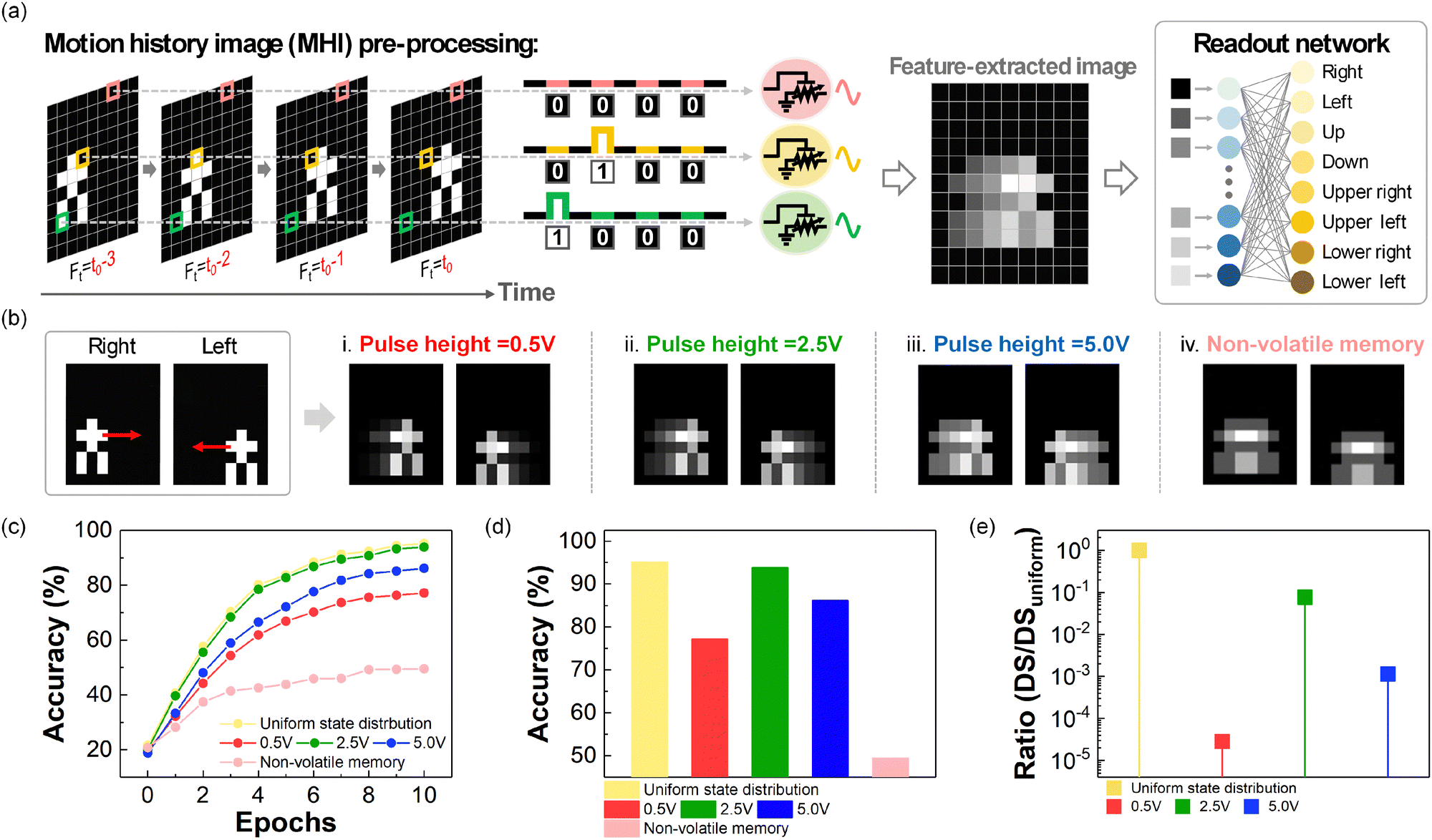 | ||
| Fig. 5 (a) Schematic illustrating the conversion of spatiotemporal information from four temporal frames into 4-bit binary electrical pulses by the IGZO TFT. The output currents recorded after the last frame are utilized as features for classification by the readout network. (b) Feature-extracted images for rightward and leftward motion classes under pulse heights of (i) 0.5 V, (ii) 2.5 V, (iii) 5.0 V, and (iv) non-volatile memory (NVM) conditions, highlighting the clarity of directional trajectories. (c) Classification accuracy as a function of training epochs for various pulse heights, with the final accuracy after 10 epochs shown in (d) and compared against the ideal uniform state distribution. (e) Normalized degree of state separation (DS) ratios relative to DSuniform, showing the correlation between state separation and classification accuracy. | ||
Fig. 5(b) and Fig. S19 (ESI†) shows the feature-extracted images for various directions under pulse heights of 0.5 V, 2.5 V, and 5.0 V, as well as the NVM condition. At a pulse height of 2.5 V, fading memory dynamics exhibited optimal performance by generating high-resolution images that accurately captured motion direction. This was achieved by ensuring a balanced interplay between the gradual fading of past frames and the integration of sequential motion data. In contrast, simulations under the NVM condition revealed that static retention dominated the response, resulting in symmetric trajectories that lacked directional information and failed to preserve historical motion patterns. Fig. S20 (ESI†) presents a comparative analysis of the classification accuracy of feature-extracted images with and without Gaussian noise. Without Gaussian noise, the accuracy at a pulse height of 2.5 V reached 96.2%, whereas the inclusion of Gaussian noise reduced it to 93.9%. Considering device inhomogeneity in practical applications, our work focuses on accuracy differences under Gaussian noise. As shown in Fig. 5(c) and (d), the highest accuracy at a pulse height of 2.5 V and an interval of 1 ms closely approaches the theoretical maximum of 95.2%, which corresponds to an ideal uniform state distribution where all 16 states are evenly spaced. At the pulse height of 0.5 V, the short memory duration in responding to the 4-bit time-series pulse streams was insufficient to retain historical information, leading to incomplete trajectory reconstruction and a lower classification accuracy of 77.2%. Conversely, at the pulse height of 5.0 V and under the simulated NVM condition, excessive memory retention resulted in overlapping state distributions, reducing the distinction between motion directions and further lowering classification accuracy to 86.2% and 49.6%, respectively. These results highlight the necessity of optimizing pulse height and interval to enhance device performance, ensuring accurate motion trajectory classification and reliable processing of time-series data.
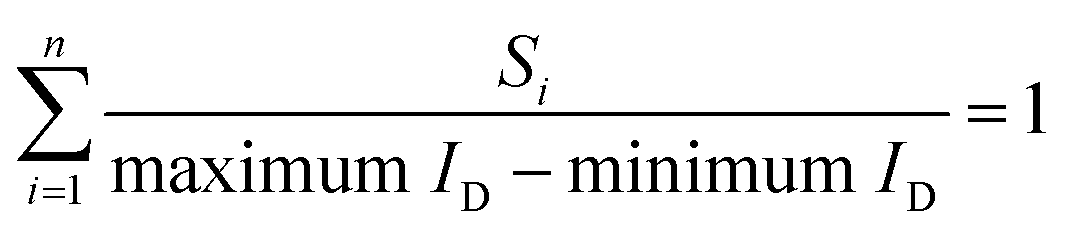
To further evaluate the classification performance and investigate the relationship between state separation and accuracy, a metric was introduced to quantify the degree of state separation (DS). The DS was defined as:52
 | (1) |
 | (2) |
In addition to evaluating the impact of state separation on the classification accuracy of the custom dataset, we further validated the practical applicability of our approach using a standard dataset. Specifically, the KTH dataset was employed for image preprocessing, comprising six action classes performed by 25 subjects across four different scenarios.53,54 For feature extraction, four frames were selected from each video and converted into binarized pixel images, with each frame containing 19![[thin space (1/6-em)]](https://www.rsc.org/images/entities/char_2009.gif) 200 pixels. Through encoding the pixels of each frame to corresponding 4-bit pulse streams and mapping to the 16 distinct conductance states, the feature-extracted images were constructed, as shown in Fig. S21 (ESI†). These feature-extracted images were then fed into a 19200 × 128 × 64 × 6 neural network for classification, achieving an accuracy of 91.7%, as illustrated in Fig. S22 (ESI†). The result indicates that our approach can be well applied to the standard dataset for motion history image preprocessing and classification.
200 pixels. Through encoding the pixels of each frame to corresponding 4-bit pulse streams and mapping to the 16 distinct conductance states, the feature-extracted images were constructed, as shown in Fig. S21 (ESI†). These feature-extracted images were then fed into a 19200 × 128 × 64 × 6 neural network for classification, achieving an accuracy of 91.7%, as illustrated in Fig. S22 (ESI†). The result indicates that our approach can be well applied to the standard dataset for motion history image preprocessing and classification.
3. Conclusions
This study demonstrates the potential of the IGZO TFT with voltage-modulated fading memory dynamics as temporal feature extractors, advancing time-series data processing and motion trajectory analysis in neural networks. By utilizing the electric-field-induced migration of oxygen vacancies within the HfOx dielectric layer, the device dynamically adjusts channel conductance in response to both input stimuli and memory dynamics, enabling effective preprocessing of motion history images. In contrast to simulations under the NVM condition, which exhibit static retention and limited ability to distinguish temporal variations, fading memory dynamics allow for a more responsive and accurate encoding of temporal correlations. The systematic evaluation of state separation, quantified using the degree of state separation (DS), highlights the importance of state differentiation in improving device performance. As the DS ratio approaches 1, the state distribution becomes more uniform, directly contributing to enhanced recognition accuracy. Experimental results show that optimizing pulse height and pulse interval applied on the IGZO TFT enables accurate motion direction classification, achieving 93.9% accuracy with feature-extracted images constructed from the well-separated 16 conductance states obtained at the optimized pulse height of 2.5 V. This optimal condition balances memory response, preserving recent inputs while preventing excessive retention that may obscure feature extraction, further reinforcing the advantages of fading memory dynamics in temporal feature extraction. These findings provide valuable insights for the development of next-generation neuromorphic architectures capable of handling complex spatiotemporal tasks with improved accuracy and efficiency.4. Experimental
4.1 Device fabrication
The IGZO TFT was fabricated on a heavily doped p-type silicon (Si) substrate with a 100-nm-thick thermally grown silicon dioxide (SiO2) layer. The substrate was cleaned with acetone, isopropanol, and deionized water to remove contaminants. The Pt gate electrode was deposited on the cleaned SiO2/p+ Si substrate using radio frequency (RF) magnetron sputtering with 100 W RF power and an argon (Ar) gas flow rate of 50 sccm at 4 torr for 5 minutes. Subsequently, HfOx dielectric layer was deposited using RF sputtering at 100 W with a gas mixture of Ar and O2 in a 4:1 ratio at 11.6 mTorr for 75 minutes. IGZO channel layer was then deposited under gas flow of 100 sccm with Ar at 10 mTorr and at an RF power of 50 W for 21 minutes. Finally, Al source and drain electrodes were deposited via e-beam evaporation using a shadow mask, defining a channel with a length and width of 80 μm.
4.2 Characterizations
The TEM images and EDS analysis were obtained using a JEM 2100F field emission transmission electron microscope. The current–voltage (I–V) characteristics of the IGZO TFT were performed with the source/measure unit (SMU) in Keysight B1500A semiconductor device parameter analyzer under ambient condition. For electrical pulsed measurements, Keysight B1530A waveform generator/fast measurement unit (WGFMU) was employed.4.3 Neural network simulations
Simulations for motion direction recognition were conducted using fully connected artificial neural network (ANN) architectures, implemented in Python. Each motion sequence comprised four temporal frames with a resolution of 9 × 11 pixels and binary pixel values (0 or 1), capturing both spatial and temporal information. These frames were processed into 99 pulse streams in a 4-bit format, which were then applied to the IGZO TFT device. The resulting current responses were recorded and used for model training and testing. A total of 8800 motion sequences were prepared, with 7040 for training and 1760 for testing. The ANN architecture consisted of 99 input neurons and 8 output neurons, corresponding to the eight motion directions: up, down, left, right, upper-right, lower-right, upper-left, and lower-left. Model training utilized feed-forward and backpropagation algorithms with the categorical cross-entropy loss function, while Softmax regression in the output layer computed the probability distribution across motion classes.Author contributions
Yu-Chieh Chen: investigation, conceptualization, data curation, formal analysis, methodology, software, validation, visualization and writing the original draft; Jyu-Teng Lin: methodology, validation and editing; Kuan-Ting Chen: methodology, validation and editing; Chun-Tao Chen: editing; Jen-Sue Chen: funding acquisition, supervision, project administration, validation and editing. All authors reviewed the manuscript.Data availability
The data supporting this article have been included as part of the ESI.†Conflicts of interest
There are no conflicts to declare.Acknowledgements
We appreciate the financial support from the National Science and Technology Council of Taiwan (Project No. NSTC 113-2223-E-006-004, NSTC 113-2124-M-006-008-MY3 and NSTC 114-2923-E-006-008-MY3).References
- Y. He, L. Zhu, Y. Zhu, C. Chen, S. Jiang, R. Liu, Y. Shi and Q. Wan, Adv. Intell. Syst., 2021, 3, 2000210 Search PubMed
.
- P. Yao, H. Wu, B. Gao, J. Tang, Q. Zhang, W. Zhang, J. J. Yang and H. Qian, Nature, 2020, 577, 641–646 CrossRef CAS PubMed
- F. Aguirre, A. Sebastian, M. Le Gallo, W. Song, T. Wang, J. J. Yang, W. Lu, M.-F. Chang, D. Ielmini, Y. Yang, A. Mehonic, A. Kenyon, M. A. Villena, J. B. Roldán, Y. Wu, H.-H. Hsu, N. Raghavan, J. Suñé, E. Miranda, A. Eltawil, G. Setti, K. Smagulova, K. N. Salama, O. Krestinskaya, X. Yan, K.-W. Ang, S. Jain, S. Li, O. Alharbi, S. Pazos and M. Lanza, Nat. Commun., 2024, 15, 1974 CAS
- M.-K. Song, J.-H. Kang, X. Zhang, W. Ji, A. Ascoli, I. Messaris, A. S. Demirkol, B. Dong, S. Aggarwal, W. Wan, S.-M. Hong, S. G. Cardwell, I. Boybat, J.-S. Seo, J.-S. Lee, M. Lanza, H. Yeon, M. Onen, J. Li, B. Yildiz, J. A. del Alamo, S. Kim, S. Choi, G. Milano, C. Ricciardi, L. Alff, Y. Chai, Z. Wang, H. Bhaskaran, M. C. Hersam, D. Strukov, H. S. P. Wong, I. Valov, B. Gao, H. Wu, R. Tetzlaff, A. Sebastian, W. Lu, L. Chua, J. J. Yang and J. Kim, ACS Nano, 2023, 17, 11994–12039 CAS
- Y. Li and K.-W. Ang, Adv. Intell. Syst., 2021, 3, 2000137 Search PubMed
- C. Wang, G. Shi, F. Qiao, R. Lin, S. Wu and Z. Hu, Nanoscale Adv., 2023, 5, 1559–1573 Search PubMed
- Y. LeCun, Y. Bengio and G. Hinton, Nature, 2015, 521, 436–444 CAS
- Y. Zhong, J. Tang, X. Li, B. Gao, H. Qian and H. Wu, Nat. Commun., 2021, 12, 408 CAS
- J. Cao, X. Zhang, H. Cheng, J. Qiu, X. Liu, M. Wang and Q. Liu, Nanoscale, 2022, 14, 289–298 CAS
- X. Duan, Z. Cao, K. Gao, W. Yan, S. Sun, G. Zhou, Z. Wu, F. Ren and B. Sun, Adv. Mater., 2024, 36, 2310704 CAS
- M. Kim, M. A. Rehman, D. Lee, Y. Wang, D.-H. Lim, M. F. Khan, H. Choi, Q. Y. Shao, J. Suh, H.-S. Lee and H.-H. Park, ACS Appl. Mater. Interfaces, 2022, 14, 44561–44571 CAS
- F. Zahoor, A. Nisar, U. I. Bature, H. Abbas, F. Bashir, A. Chattopadhyay, B. K. Kaushik, A. Alzahrani and F. A. Hussin, Nanoscale Adv., 2024, 6, 4980–5006 Search PubMed
- D. P. Sahu, K. Park, P. H. Chung, J. Han and T.-S. Yoon, Sci. Rep., 2023, 13, 9592 CAS
- I. Boybat, M. Le Gallo, S. R. Nandakumar, T. Moraitis, T. Parnell, T. Tuma, B. Rajendran, Y. Leblebici, A. Sebastian and E. Eleftheriou, Nat. Commun., 2018, 9, 2514 Search PubMed
- S. R. Nandakumar, M. Le Gallo, I. Boybat, B. Rajendran, A. Sebastian and E. Eleftheriou, J. Appl. Phys., 2018, 124, 152135 Search PubMed
- S. H. Sung, T. J. Kim, H. Shin, T. H. Im and K. J. Lee, Nat. Commun., 2022, 13, 2811 CrossRef CAS PubMed
- S. Wang, L. Liu, L. Gan, H. Chen, X. Hou, Y. Ding, S. Ma, D. W. Zhang and P. Zhou, Nat. Commun., 2021, 12, 53 CrossRef CAS PubMed
- F.-J. Chu, Y.-C. Chen, L.-C. Shih, S.-C. Mao and J.-S. Chen, Adv. Funct. Mater., 2024, 34, 2310951 CrossRef CAS
- Z.-D. Luo, S. Zhang, Y. Liu, D. Zhang, X. Gan, J. Seidel, Y. Liu, G. Han, M. Alexe and Y. Hao, ACS Nano, 2022, 16, 3362–3372 CAS
- N. Mohta, A. Rao, N. Remesh, R. Muralidharan and D. N. Nath, RSC Adv., 2021, 11, 36901–36912 RSC
- Y. Choi, J.-H. Kim, C. Qian, J. Kang, M. C. Hersam, J.-H. Park and J. H. Cho, ACS Appl. Mater. Interfaces, 2020, 12, 4707–4714 CrossRef CAS PubMed
- J.-M. Yu, C. Lee, D.-J. Kim, H. Park, J.-K. Han, J. Hur, J.-K. Kim, M.-S. Kim, M. Seo, S. G. Im and Y.-K. Choi, Adv. Funct. Mater., 2021, 31, 2010971 CrossRef CAS
- Y. Du, W. Xiao, G. Miao, Z. Yin, R. Ci, G. Liu and F. Shan, J. Mater. Chem. C, 2025, 13, 1318–1324 RSC
- T. Böhnert, Y. Rezaeiyan, M. S. Claro, L. Benetti, A. S. Jenkins, H. Farkhani, F. Moradi and R. Ferreira, Commun. Eng., 2023, 2, 65 Search PubMed
- J. R. Mohan, A. J. Mathew, K. Nishimura, R. Feng, R. Medwal, S. Gupta, R. S. Rawat and Y. Fukuma, Sci. Rep., 2023, 13, 7909 CAS
- J. Jeong, Y. Jang, M.-G. Kang, S. Hwang, J. Park and B.-G. Park, Adv. Electron. Mater., 2024, 10, 2300889 CAS
- G. Zhang, J. Qin, Y. Zhang, G. Gong, Z.-Y. Xiong, X. Ma, Z. Lv, Y. Zhou and S.-T. Han, Adv. Funct. Mater., 2023, 33, 2302929 CAS
- S.-O. Park, H. Jeong, J. Park, J. Bae and S. Choi, Nat. Commun., 2022, 13, 2888 CAS
- A. H. Jaafar, L. Shao, P. Dai, T. Zhang, Y. Han, R. Beanland, N. T. Kemp, P. N. Bartlett, A. L. Hector and R. Huang, Nanoscale, 2022, 14, 17170–17181 CAS
- H. Park, D. Ju, C. Mahata, A. Emelyanov, M. Koo and S. Kim, Adv. Electron. Mater., 2024, 10, 2300911 CAS
- N. V. Prudnikov, V. A. Kulagin, S. Battistoni, V. A. Demin, V. V. Erokhin and A. V. Emelyanov, Phys. Status Solidi A, 2023, 220, 2200700 CAS
- A. Gaurav, X. Song, S. Manhas, A. Gilra, E. Vasilaki, P. Roy and M. M. De Souza, Front. Electron., 2022, 3, 869013 Search PubMed
- J. Yang, H. Cho, H. Ryu, M. Ismail, C. Mahata and S. Kim, ACS Appl. Mater. Interfaces, 2021, 13, 33244–33252 CAS
- H. So, J. Lee, C. Mahata, S. Kim and S. Kim, Adv. Mater. Technol., 2024, 9, 2301390 CAS
- H. Lee, J. Oh, W. Ahn, M. Kang, S. Park, H. Kim, S. Yoo, B. C. Jang and S.-Y. Choi, Adv. Funct. Mater., 2024, 2416811 Search PubMed
- R. Chen, H. Yang, R. Li, G. Yu, Y. Zhang, J. Dong, D. Han, Z. Zhou, P. Huang, L. Liu, X. Liu and J. Kang, Sci. Adv., 2024, 10, eadl1299 CAS
- C. Gao, D. Liu, C. Xu, W. Xie, X. Zhang, J. Bai, Z. Lin, C. Zhang, Y. Hu, T. Guo and H. Chen, Nat. Commun., 2024, 15, 740 CAS
- H. Tan and S. van Dijken, Nat. Commun., 2023, 14, 2169 CAS
- J. Zha, Y. Xia, S. Shi, H. Huang, S. Li, C. Qian, H. Wang, P. Yang, Z. Zhang, Y. Meng, W. Wang, Z. Yang, H. Yu, J. C. Ho, Z. Wang and C. Tan, Adv. Mater., 2024, 36, 2308502 CAS
- S. Kim, J. Kim, D. Kim, J. Kim and S. Kim, APL Mater., 2023, 11, 101102 CAS
- L.-P. Feng, Z.-T. Liu and Y.-M. Shen, Vacuum, 2009, 83, 902–905 CAS
- C. V. Ramana, K. K. Bharathi, A. Garcia and A. L. Campbell, J. Phys. Chem. C, 2012, 116, 9955–9960 CrossRef CAS
- J. H. Q. Palhares, Y. Beilliard, F. Alibart, E. Bonturim, D. Z. de Florio, F. C. Fonseca, D. Drouin and A. S. Ferlauto, Nanotechnology, 2021, 32, 405202 CrossRef CAS PubMed
- T. Guo, T. Tan, Z. Liu and B. Liu, J. Alloys Compd., 2016, 686, 669–674 CrossRef CAS
- R. Zhang, H. Huang, Q. Xia, C. Ye, X. Wei, J. Wang, L. Zhang and L. Q. Zhu, Adv. Electron. Mater., 2019, 5, 1800833 CrossRef
- K.-T. Chen, L.-C. Shih, S.-C. Mao and J.-S. Chen, ACS Appl. Mater. Interfaces, 2023, 15, 9593–9603 CrossRef CAS PubMed
- C. Liu, X. Shen, S. Fan, T. Xu, J. Zhang and J. Su, ACS Appl. Electron. Mater., 2023, 5, 4657–4666 CrossRef CAS
- P. Yang, H. Jun Kim, H. Zheng, G. Won Beom, J.-S. Park, C. Jung Kang and T.-S. Yoon, Nanotechnology, 2017, 28, 225201 CrossRef PubMed
- Y. Zhou, J. Li, Y. Yang, Q. Chen and J. Zhang, ACS Appl. Mater. Interfaces, 2020, 12, 980–988 CrossRef CAS PubMed
- H. Park, S. Oh, S.-H. Jeong, O. Kwon, H. Y. Seo, J.-D. Kwon, Y. Kim, W. Park and B. Cho, ACS Appl. Electron. Mater., 2022, 4, 2923–2932 CrossRef CAS
- H. Y. Jang, O. Kwon, J. H. Nam, J.-D. Kwon, Y. Kim, W. Park and B. Cho, ACS Appl. Mater. Interfaces, 2022, 14, 52173–52181 CrossRef CAS PubMed
- S. A. Mun, Y. H. Jang, J. Han, S. K. Shim, S. Kang, Y. Lee, J. Choi, S. Cheong, S. H. Lee, S. K. Ryoo, J.-K. Han and C. S. Hwang, ACS Appl. Mater. Interfaces, 2024, 16, 42884–42893 CrossRef CAS PubMed
- C. Schuldt, I. Laptev and B. Caputo, presented in part at the Proceedings of the 17th International Conference on Pattern Recognition (ICPR), 2004.
- R. Savran Kızıltepe, J. Q. Gan and J. J. Escobar, Neural Comput. Appl., 2023, 35, 24513–24524 CrossRef
Footnote |
| † Electronic supplementary information (ESI) available. See DOI: https://doi.org/10.1039/d5nh00040h |
| This journal is © The Royal Society of Chemistry 2025 |