
Edge-induced selective etching of bilayer MoS2 kirigami structures via a space-confined method†
Weijie
Ma‡
ab,
Qing
Zhang‡
abd,
Jie
Zhu
ab,
Yang
Guo
ab,
Yajing
Sun
abf,
Lin
Li
ce and
Dechao
Geng
 *abef
*abef
aKey Laboratory of Organic Integrated Circuit, Ministry of Education & Tianjin Key Laboratory of Molecular Optoelectronic Sciences, Department of Chemistry, School of Science, Tianjin, 300072, China. E-mail: gengdechao_1987@tju.edu.cn
bCollaborative Innovation Center of Chemical Science and Engineering (Tianjin), Tianjin, 300072, China
cCollege of Chemistry, Tianjin Normal University, Tianjin, 300387, China
dSchool of Advanced Materials, Peking University Shenzhen Graduate School, Peking University, Shenzhen, 518055, China
eBeijing National Laboratory for Molecular Sciences, Beijing, 100190, China
fHaihe Laboratory of Sustainable Chemical Transformations, Tianjin, 300192, China
First published on 13th March 2025
Abstract
The controllable preparation of edge arrangements, particularly the customization of zigzag edges on demand, remains elusive. Here, a selective etching strategy to directly regulate Mo-zigzag and S-zigzag edges of MoS2 kirigami structures is proposed, paving the way for edge engineering of 2D materials and providing promising candidates for next-generation optoelectronics.
New conceptsWhile etching as a reverse process of growth has been studied for a while now, the precise synthesis of distinct edges by etching still remains a great challenge. In this work, we establish a bridge between macroscopic growth conditions and microscopic atomic arrangements by selectively obtaining molybdenum-zigzag and sulfur-zigzag edges of MoS2 kirigami structures through a space-confined etching strategy. Here an anodized molybdenum foil is employed, rather than traditional MoO3 powder, to provide a more steady precursor feeding, enabling a precise modulation of the relative concentration between Mo atoms and S atoms. It is intriguing that S-zigzag edges exhibit an etching tendency in a Mo-sufficient environment constructed by confining the space between the substrate and the Mo foil, while Mo-zigzag edges display an etching tendency in a Mo-deficient environment by increasing the space. The terminal atoms are characterized by atomic-resolution STEM and DFT calculations support the growth mechanism in which the precursor concentration will determine the energy of different atom-zigzag edges. The successful synthesis of edge-rich kirigami structures holds promising potential for novel 2D platforms in electronics, optics, and catalysis. This work offers fresh insights into the fabrication of complex 2D architectures and further expands the applications of distinct edge structures. |
Introduction
As an indispensable member of the two-dimensional (2D) layered material family, transition metal dichalcogenides (TMDs) have a more abundant electronic band structure than traditional graphene, exhibiting innovative physical and chemical properties.1 Thus, TMDs have broad applications in electronics,2 photoelectronics,3 catalysis,4etc. Currently, a wide variety of TMDs with a distinct morphology, domain size, and layer number can be realized via chemical vapor deposition (CVD).5–7 However, the research on the performance and preparation of its one-dimensional (1D) edges is still in a preliminary stage.The 1D edges of the 2D materials are equivalent to the surfaces of the bulk materials, showing significantly different properties from the inert 2D basal plane,8 such as stronger nonlinear optical response,9 higher catalytic activity,10 larger range of work functions,11 and the emergence of magnetism.12 The intrinsic edges of hexagonal 2D materials are zigzag and armchair-shaped, playing a pivotal role in regulating final morphology and functionalities.13–15 Therefore, the manipulation of 1D edges opens up a larger application market for 2D materials. Notably, TMDs have more complex atom terminals than single-atom graphene due to their sandwich crystal structure, containing a chalcogenide-terminated zigzag edge, a transition metal element-terminated zigzag edge, and an armchair edge,16 which poses a challenge for the selective preparation of edge structures.
Etching as a reverse process of CVD growth not only helps to reveal the growth mechanism comprehensively but also provides many novel architectures for excavating hidden properties of 2D materials.8,17,18 At present, etching has shown great potential in the field of edge engineering. For example, the modulation of the flow rate of hydrogen facilitated the emergence of multi-stage etched patterns of graphene and its heterostructures.17–19 Moreover, Zhang et al. demonstrated that anisotropic etching of MoSe2 can be carried out with the aid of oxygen plasma, which provides a novel platform with high-density edges for optoelectronic devices.20 Huang et al. prepared etching patterns using different atomic terminals via laser irradiation and thermal annealing treatment, which has great application potential in catalysis, integrated circuits, and nonlinear optics.21 It is worth mentioning that the introduction of an etchant, laser, or plasma has brought irreversible degradation to the material, restricting its further application.22 Jin's group created WSe2 kirigami structures with edge-rich morphology using a non-destructive preparation method.23 They found that the etching behavior is affected by the stacking configuration of the bottom trilayer.
Although some edge-rich architectures can be created by etching, there is a lack of precise control of the atomic arrangement of the edge. Therefore, it is highly desired that the edge-rich structures be studied in depth with emphasis on the control of 1D edges to meet the market demand.
Here, we report a selective etching method to directly fabricate edge-rich bilayer MoS2 kirigami structures with distinct atom terminals, which establishes a bridge between atomic arrangement and etching conditions. Our experiments observed that the S-zigzag and Mo-zigzag show different etching tendencies in distinct growth microenvironments achieved using the space-confined method. The S-zigzag edges are prone to etching in a Mo-sufficient atmosphere by confining the space between the Mo foil and the substrate, while both Mo-zigzag and S-zigzag tend to be etched in a Mo-deficient atmosphere by increasing the space between the Mo foil and the substrate, leading to the formation of distinct morphology, namely the Mo-zigzag structure and the Mo/S-zigzag structure. Theoretical calculations further prove the experimental results. Employing the Mo foil facilitates the formation of bilayer MoS2 and allows the control of the precursor concentration,7,24,25 paving the way for subsequent two types of etching behavior of bilayer MoS2 kirigami structures. Aberration-corrected scanning transmission electron microscopy (STEM) is utilized to validate the atomic arrangement of the etched edges and stacking configuration of as-etched samples, which is also verified in second-harmonic generation (SHG) measurements. This edge-rich MoS2 kirigami structure fabricated by the selective etching process offers an alternative 2D research platform for catalysis, nonlinear optics, and electronics, opening up new avenues for CVD in the field of 1D edge engineering.
Results and discussion
Edge-rich bilayer MoS2 kirigami structures were constructed using a selective etching process established via the space-confined method to adjust the precursor concentration, which exhibited ideal reproducibility (Fig. S1, ESI†). The specific evolution manner of structures can be divided into two stages, depicted in Fig. 1. In contrast to the conventional triangular morphology, the hexagram-shaped first layers were synthesized in the initial growth stage (Fig. S2, ESI†). The second layers have exhibited distinct morphology by altering the supply of Mo to establish different growth microenvironments during the etching stage. In brief, the second layer of MoS2 structures, which was originally hexagonal with alternating Mo-zigzag and S-zigzag edges, has been selectively etched at different atmospheres (shown in Fig. S3 and S4, ESI†). In a microenvironment with sufficient Mo, achieved by confining the space between the Mo foil and the substrate, the three S-zigzag edges tend to be etched and concave inward, leaving the Mo-zigzag edges intact (Fig. 2a–d). Under the Mo-deficient conditions, achieved by increasing the space between the Mo foil and the substrate, the S-zigzag edge and the Mo-zigzag edge have the same etching tendency, leading to the formation of a Mo/S-zigzag structure (Fig. 2e–h). Through this basic growth and etching process, two edge-rich structures of MoS2, expected to be applied in the field of catalysis, have been successfully constructed.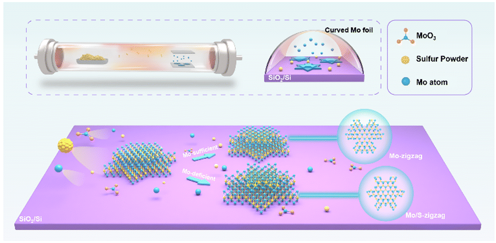 | ||
| Fig. 1 Schematic illustration of the selective etching of bilayer MoS2 kirigami structures on the SiO2/Si substrate. The bilayer MoS2 consists of a hexagram-shaped first layer and a distinct second layer. The S-zigzag edges will be etched in a Mo-sufficient atmosphere, and the Mo/S-zigzag edges will be etched in a Mo-deficient atmosphere. | ||
 | ||
| Fig. 2 Morphologic and structural characterization of bilayer MoS2 kirigami structures. OM (a) and (e), SEM (b) and (f), AFM (c) and (g), and Raman mapping (d) and (h) results for two kinds of structures. Scale bars of (a)–(d) are 5 μm, 5 μm, 2 μm, and 3 μm, respectively. All scale bars of (e)–(h) are 5 μm. (i) Raman spectra of the MoS2 measured at the three points selected in (a). The corresponding PL spectra are shown in (j). (k) is the XPS core levels of Mo 3d. | ||
On the basis of Burton–Cabrera–Frank (BCF) theory, the crystal shape is determined by the dominant crystal face which has a faster growth rate.26 In terms of 2D materials, the final morphology relies on the growth rate of different edges.27 It has been reported that the supersaturation level of the local growth environment, essentially related to the growth rate of the edge,28 can be regulated by adjusting the S![[thin space (1/6-em)]](https://www.rsc.org/images/entities/char_2009.gif) :Mo ratio and the growth temperature, so the morphologies of triangles, hexagons, and their intermediate states with desired S-zigzag edges or Mo-zigzag edges can be designed in this way. For instance, the morphology is a hexagon with Mo-zigzag and S-zigzag edges alternately when S:Mo = 2.29 The Mo-terminated triangle morphology is more competitive in a Mo-rich atmosphere because sufficient Mo will combine with the exposed S-terminal atoms, causing the S-zigzag edge to rapidly grow until it vanishes.30 Conversely, a deficient Mo atmosphere will ultimately result in the formation of a triangular morphology with three S-zigzag edges.24 Thus, different local growth environments were established to construct distinct structures of MoS2, which is realized by designing the spacing between Mo foil and substrate in this work, as shown in Fig. S5 (ESI†). Molybdenum trioxide (MoO3) powder, as the most common solid precursor for the growth of MoS2, has a rapid sublimation process during the heating step, hindering the control of the precursor concentration.31 Therefore, an electrochemically oxidized Mo foil was exploited as the precursor to achieve a continuous and stable feeding of Mo sources.7,24,25 X-ray photoelectron spectroscopy (XPS) results confirmed that the anodized Mo foil possesses richer valence states (from IV to VI) than MoO3 powder. (Fig. S6, ESI†). The energy-dispersive X-ray spectroscopy of pre-growth Mo foil and after-growth Mo foil indicates the effective feeding of Mo atoms (Fig. S7, ESI†). Apart from the precursor concentration, growth temperature and etching time are other important factors.32 The etching process was completed by skillfully adjusting the temperature and etching time without any damage to the samples in this work. It was found that the reaction can be carried out in the direction of etching by raising the temperature.33,34 However, prolonged exposure to high temperatures will give rise to excessive etching, which could cause the material to crack or even vanish (shown in Fig. S8 and S9, ESI†). After parameter optimization, the selective etching finally proceeded at 980 °C for 10 min under 60 sccm Ar flow.
:Mo ratio and the growth temperature, so the morphologies of triangles, hexagons, and their intermediate states with desired S-zigzag edges or Mo-zigzag edges can be designed in this way. For instance, the morphology is a hexagon with Mo-zigzag and S-zigzag edges alternately when S:Mo = 2.29 The Mo-terminated triangle morphology is more competitive in a Mo-rich atmosphere because sufficient Mo will combine with the exposed S-terminal atoms, causing the S-zigzag edge to rapidly grow until it vanishes.30 Conversely, a deficient Mo atmosphere will ultimately result in the formation of a triangular morphology with three S-zigzag edges.24 Thus, different local growth environments were established to construct distinct structures of MoS2, which is realized by designing the spacing between Mo foil and substrate in this work, as shown in Fig. S5 (ESI†). Molybdenum trioxide (MoO3) powder, as the most common solid precursor for the growth of MoS2, has a rapid sublimation process during the heating step, hindering the control of the precursor concentration.31 Therefore, an electrochemically oxidized Mo foil was exploited as the precursor to achieve a continuous and stable feeding of Mo sources.7,24,25 X-ray photoelectron spectroscopy (XPS) results confirmed that the anodized Mo foil possesses richer valence states (from IV to VI) than MoO3 powder. (Fig. S6, ESI†). The energy-dispersive X-ray spectroscopy of pre-growth Mo foil and after-growth Mo foil indicates the effective feeding of Mo atoms (Fig. S7, ESI†). Apart from the precursor concentration, growth temperature and etching time are other important factors.32 The etching process was completed by skillfully adjusting the temperature and etching time without any damage to the samples in this work. It was found that the reaction can be carried out in the direction of etching by raising the temperature.33,34 However, prolonged exposure to high temperatures will give rise to excessive etching, which could cause the material to crack or even vanish (shown in Fig. S8 and S9, ESI†). After parameter optimization, the selective etching finally proceeded at 980 °C for 10 min under 60 sccm Ar flow.
Optical microscopy (OM) and scanning electron microscopy (SEM) images clearly show two different kirigami structures, namely, the Mo-zigzag structure (Fig. 2a and b) and the Mo/S-zigzag structure (Fig. 2e and f). We found that these two structures are composed of the approximate hexagram-shaped first layer and a distinctly different second layer, both having more abundant edges than traditional triangles. The first layer is not identical may be attributed to the variation in the edge growth rate according to the classical crystal growth theory mentioned above, which directly affects the symmetry of the second layer. The symmetrical second etching layer is likely to form on top of the symmetrical first layer looking like a flower, as shown in Fig. S10a–d (ESI†). Nevertheless, when the bottom layer is asymmetric, the shape of the etching layer is also asymmetric (Fig. S10e–h, ESI†). Furthermore, the etching area will gradually increase inward with time, resulting in a morphological evolution of the second layer from a complete hexagon to a pinwheel (Fig. S11, ESI†). Atomic force microscopy (AFM) proved the double-layer feature of as-etched structures. The inset height profiles confirmed the thickness of each layer is approximately 0.7 nm, corresponding to the single-layer MoS2 (Fig. 2c and g).2
To investigate the quality of as-etched MoS2 kirigami structures, Raman and PL measurements were performed at three points marked in Fig. 2a, referring to the first layer, etched area, and second layer (data for the Mo/S-zigzag structure are shown in Fig. S12, ESI†). Raman results of point 1 and point 2 present the same featured peaks, located at 381 cm−1 (in-plane vibrations of Mo and S atoms, E12g) and 403 cm−1 (out-of-plane vibration of Mo and S atoms, A1g).11 Raman A1g–E12g splitting of about22 cm−1 revealed the monolayer properties of the first layer and etched area.6,7 The A1g and E12g peaks of the second layer exhibit a slight red shift and blue shift, respectively, while the frequency difference of these two peaks increases to 25 cm−1, which is consistent with the characteristics of bilayer MoS2 (Fig. 2i).7 The frequency shifts of the E12g and A1g modes can be attributed to interlayer coupling and dielectric screening effects. In bilayer MoS2, the van der Waals interactions between layers enhance the coupling of in-plane and out-of-plane vibrations, resulting in a decrease in the E12g mode frequency and an increase in the A1g mode frequency. Consequently, the peak spacing between these two modes is significantly enlarged.35 Fig. S13 (ESI†) presents the comparative analysis of the etched and unetched regions across different samples. The characteristic E12g and A1g modes in the monolayer and bilayer region, both show peak position variations of less than 0.5 cm−1, confirming the minimal impact of defects on vibrational properties, as shown in Fig. S13c (ESI†). Fig. S13d (ESI†) shows an increased peak spacing, confirming the coupling effect between the bilayer MoS2 structures. Meanwhile, it has been reported that applying strain to MoS2 can induce splitting of the E12g mode into an E' peak. However, the distinct E12g peaks observed in Fig. 2 and Fig. S12 and S13 (ESI†) demonstrate the absence of additional strain in our material. Ultra-low-frequency Raman spectroscopy provides a powerful probe for characterizing the relative vibrations between layers in 2D materials. By analyzing the in-plane shear modes (S) and out-of-plane breathing modes (B), it is possible to investigate the interlayer coupling, stacking configurations, and twist angles.36 As shown in Fig. S14 (ESI†), the Raman spectra of the unetched region exhibit a sharp shear peak at 22 cm−1 and a broad breathing peak at 40 cm−1, which are characteristic of the 2H phase of MoS2. This confirms that the two layers are stacked at a 60° twist angle. In contrast, the etched region is the monolayer MoS2, which lacks the characteristic peaks associated with layer-layer vibrations due to the absence of additional layers. Fig. S15 (ESI†) presents the temperature dependence Raman spectra of MoS2 kirigami structures aged for 12 months. Across the temperature range of 80 K to 300 K, the E12g (381 cm−1) and A1g (405 cm−1) characteristic peaks exhibit only minor shifts attributed to the increase of bond length caused by thermal expansion, demonstrating the structural stability and holding promising potential for practical applications. For point 3, an A1g Raman peak mapping was carried out to demonstrate the uniformity of two edge-rich structures. Both of these etched structures have a sharp boundary, indicating the high quality of as-etched samples (Fig. 2d and h).
Fig. 2j displays PL for three different regions (points 1, 2, and 3). A prominent peak at 1.78 eV, which corresponds to the A exciton of MoS2, is detected in the PL spectra of the bottom layer (point 1) and etched area (point 2).2 The broad peak at 1.93 eV is correlated to the resonance of B exciton. As shown in Fig. S16 (ESI†), the A and B excitons in MoS2 arise from the Coulomb-bound electron–hole pairs, where the A exciton originates from the direct optical transition between the conduction band minimum (CBM) and the upper spin–orbit split valence band. In contrast, the B exciton is formed by the transition between the CBM and the lower spin–orbit split valence band, with an energy separation of approximately 150–200 meV due to strong spin–orbit coupling effects in the valence band.37 Points 1 and 2 exhibit similar intensities, both consistent with the characteristics of monolayer MoS2. In contrast, the intensities of both A and B excitons at point 3 are reduced, with the A exciton showing a more pronounced decrease in intensity, which aligns with the results observed for bilayer MoS2.35 Fig. S17 (ESI†) presents a detailed analysis of the PL spectra for points 2 and 3. Through intensity integration, it is observed that the intensities of both A and B excitons decrease, with the A exciton exhibiting a reduction of nearly 50%, which induced by the band gap transition from direct to indirect, in line with the results of bilayer MoS2.7 Zhang et al. have pointed out in earlier research that there are differences in the PL intensity of different atomic terminals.21 Oxygen is more likely to form chemisorption with Mo atoms than with S atoms, resulting in a stronger PL signal at the Mo-terminal edge. However, since the edge-rich structure we prepared in this work is a bilayer, the results of PL measurement cannot exclude the enormous impact of the bandgap transition. Therefore, the atomic terminal-dependent PL intensity is not observed. In this work, STEM as the most powerful evidence was adopted to identify the atomic termination of the etching edge at the atomic scale, which is explained in more detail later. Kelvin probe force microscopy (KPFM) shows a different surface potential between monolayer and bilayer regions, as shown in Fig. S18 (ESI†).
The large-area successful preparation of structures allows the XPS characterization to define the chemical states of Mo and S. A XPS survey scan is provided in Fig. S19a (ESI†), where the peaks of O and Si are from the substrate, and the peak of C is from the contaminant. Two peaks can be observed at 232.71 eV and 229.58 eV in the XPS core level of Mo 3d, which correspond to Mo 3d3/2 and Mo 3d5/2, respectively (Fig. 2k). In the XPS core level of S 2p, the two peaks that appeared at 163.57 eV and 162.38 eV are related to S 2p1/2 and S 2p3/2, respectively (Fig. S19b, ESI†). These peaks are consistent with the previously reported standard values without any peak shift,2 implying that the etching does not affect the chemical environment of the atoms.
Both of these etched structures originate from a hexagon with alternating three Mo-zigzag edges and three S-zigzag edges.29 In the reaction atmosphere with sufficient Mo, excessive Mo atoms serve as an etchant to etch the S-zigzag edges toward the center, leaving three straight Mo-zigzag edges, and finally forming a Mo-zigzag kirigami structure (as shown in Fig. 3a). Meanwhile, the etching tendency of the S-zigzag edge and the Mo-zigzag edge is consistent in a Mo-deficient atmosphere, both of which will be concave to the center and finally evolve from a hexagon to an irregular Mo/S-zigzag structure, forming edges with multiple atomic terminals (as shown in Fig. S20a, ESI†).30
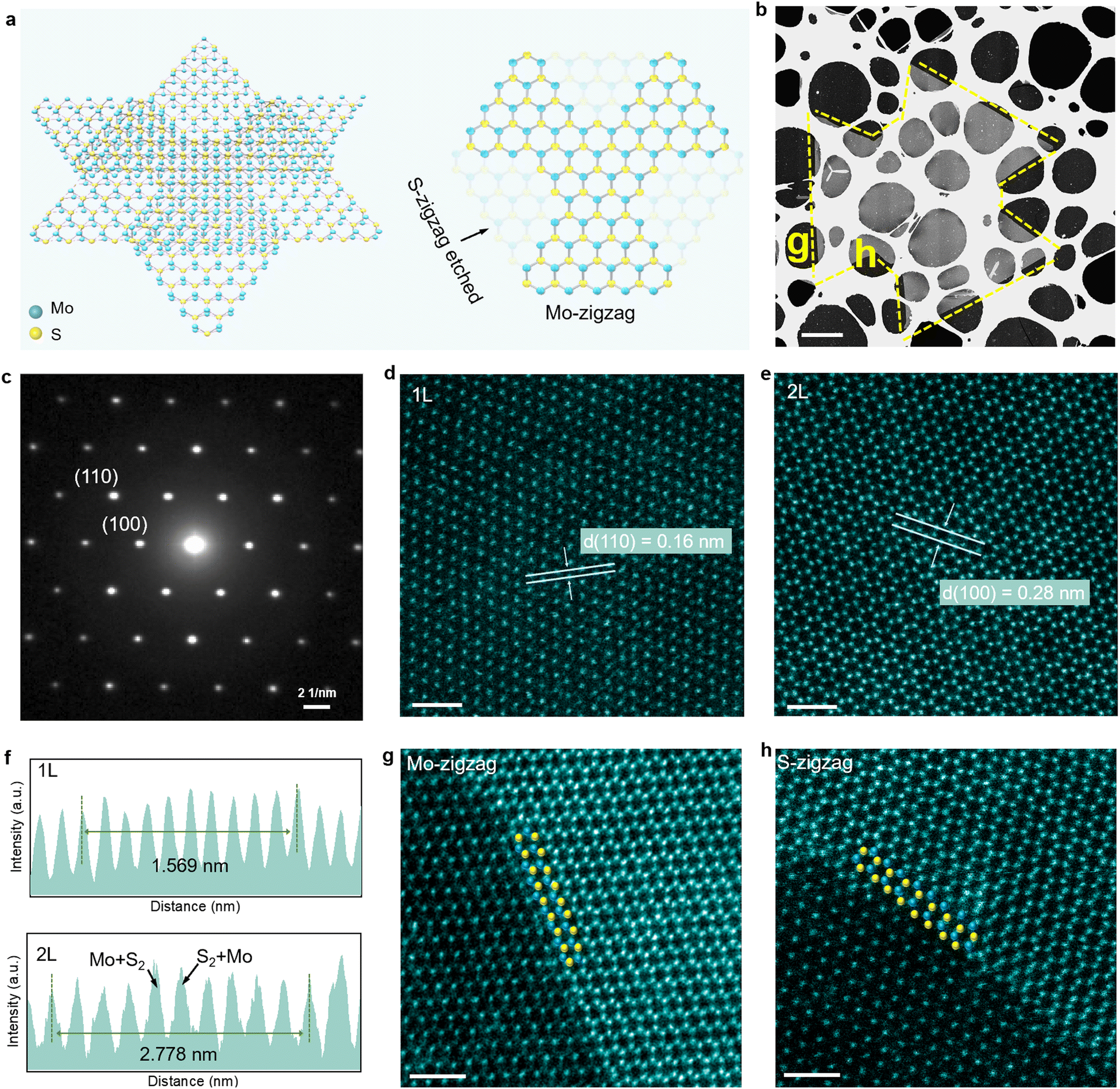 | ||
| Fig. 3 Atomic-resolution HAADF-STEM images of the etched edges of two kirigami structures. (a) Atomic diagrams of Mo-zigzag structure. (b) Low-magnification dark-field image of the Mo-zigzag structure. (c) Selected area low energy electron diffraction (SAED) patterns of bilayer region. (d) and (e) HAADF-STEM images selected randomly in the monolayer and bilayer regions. (f) The corresponding intensity profile obtained in (d) and (e) along the blue lines. (g) and (h) HAADF-STEM images of straight edge and etched edge marked in (b). Scale bar of (b) is 1 μm and scale bars of (d), (e), (g), and (h) are 1 nm. | ||
To verify this hypothesis, an atomic resolution STEM is exploited to unravel the atomic arrangement, crystal quality, and stacking configuration of the kirigami structures. Fig. 3b shows that the intact sample is transferred to the TEM grids by the wet transfer method for subsequent observation of the atomic arrangement of the etching edges. The selected area low energy electron diffraction (SAED) image of the bilayer region (Fig. 3c) only contains a set of hexagonal diffraction points, signifying the single crystal feature of structures and the absence of twist angle between the layers.2 The high-angle annular dark field (HAADF)-STEM images obtained from monolayer and bilayer regions show a clear honeycomb structure (Fig. 3d and e), where Mo atoms are represented by bright atoms, and S atoms by dark atoms.21 The HAADF-STEM of the bilayer region exhibits an ideal hexagonal lattice, and the corresponding intensity profile has the analogous intensity at each atomic column (Fig. 3f), suggesting that MoS2 is stacked in the 2H phase.6 The lattice spacings measured are 0.27 nm and 0.16 nm, which are identical to the hexagonal MoS2 crystal planes (100) and (110), respectively.2 Subsequently, we selected the straight edge and the etched edge from the Mo-zigzag structure for atomic resolution level characterization. The results reveal that the straight edge (unetched) is terminated by Mo-zigzag (Fig. 3g) and the etched area is terminated by S-zigzag (Fig. 3h), demonstrating that different atomic edges were selectively etched. For the Mo/S-zigzag structure, the Mo-zigzag terminal edge and S-zigzag terminal edge are both etched inward (Fig. S20c and d, ESI†). It is worth noting that each bright spot in bilayer 2H-MoS2 STEM images represents one Mo atom and two S atoms with comparable intensity, making the identification of terminal atoms difficult. Fig. S21 (ESI†) shows how we identified the terminal atoms at the etching boundary and more STEM images of different edges are provided in Fig. S22 (ESI†). Sulfur vacancies represent the most prevalent type of intrinsic defects in MoS2, exerting a significant influence on their electronic and optical properties.38 As illustrated in Fig. S23 (ESI†), large-area scanning STEM images reveal only a sparse distribution of sulfur vacancies, which substantiates the high crystalline quality of the MoS2 kirigami structures.
We implemented first-principles calculations based on density functional theory (DFT) within the Vienna ab initio simulation package (VASP) to further validate experimental results and identify the stable configurations of MoS2 under various concentrations of Mo and S. We utilized the Perdew–Burke–Ernzerhof (PBE) functional to address exchange–correlation interactions and employed a plane-wave cutoff energy of 450 eV for structural optimization. Additionally, we set a 1 × 1 × 1 Gamma k-point grid and an energy convergence threshold of 10−3 eV. For different boundary configurations of MoS2, we simulated five different environments of Mo and S concentrations (ratios of 0:2, 1:2, 2:2, 3:2, and 5:2), as shown in Fig. 4a and Fig. S24 (ESI†). We conducted detailed calculations of the total energy for these systems, and found that at Mo-deficient concentrations, the total energies of the Mo-zigzag and S-zigzag structures are similar, indicating comparable stability. As the Mo concentration increases, the total energies of these two structures begin to diverge significantly, with the Mo-zigzag structure having lower energy, suggesting greater stability (as shown in Fig. 4b). We also analyzed the average atomic energy of the systems (as shown in Fig. 4c), with results indicating that the Mo-zigzag structure becomes more stable as the Mo concentration increases. These theoretical calculations are consistent with the data obtained from our experiments, indicating that S-zigzag is more prone to be etched under a sufficient Mo atmosphere to form a Mo-zigzag structure.
 | ||
| Fig. 4 (a) Top views of the Mo-zigzag structure at Mo and S concentration ratios of 1:2, 2:2, and 5:2. (b) Changes in the total energy of the Mo-zigzag and S-zigzag configurations as the concentrations of Mo and S vary. (c) Changes in the average atomic energy of the Mo-zigzag and S-zigzag configurations as the concentrations of Mo and S vary. | ||
SHG is employed to evaluate the quality and stacking configuration of as-etched kirigami structures. SHG signals can be observed in non-centrosymmetric structures, such as monolayer MoS2, but disappear in centrosymmetric structures, such as the 2H phase MoS2.39 Therefore, SHG mapping images show that the intensity of the stacking area is consistent with that of the SiO2/Si substrate, and SHG appears in the non-overlapping area of the monolayer region, indicating that the structures are 2H phase (Fig. 5b and Fig. S25, ESI†). Compared with the stacking area, the monolayer region without inversion symmetry has a satisfactory SHG response. The SHG emission frequency in the monolayer region is twice the incident frequency (Fig. 5c). Meanwhile, different SHG signals arise at 532 nm when the excitation power is varied and the excitation wavelength is fixed at 1064 nm (Fig. 5d). Fig. 5e shows an expected double logarithmic curve of excitation power-dependent SHG intensity with a slope of 1.84, conveying the second-order nonlinear optical process.39 We further performed polarized SHG measurements on the monolayer region, confirming that this edge-rich MoS2 kirigami structure has a hexagonal lattice (Fig. 5f).40 In summary, the SHG behavior in different regions once again verifies the results of STEM, that is, the kirigami structures are 2H-phase, and the underlying hexagram-shaped MoS2 are monolayer. Field effect transistors based on these structures display a high on/off ratio of approximately 108, which is comparable to the reported value,2 indicating that the etching behavior does not destroy the quality of the crystal (as shown in Fig. S26a and b, ESI†). We further tested its optoelectric performance under different wavelengths of light sources. Fig. S26d–f (ESI†) show that the device has an expected optoelectric response in a wide wavelength range, whose Ioff increased with light power.
 | ||
| Fig. 5 SHG characterization of the bilayer MoS2 kirigami structures under a 1064 nm excitation laser. (a) Schematic diagram of the generation of SHG in MoS2. (b) SHG mapping of a Mo-zigzag structure. Scale bar is 6 μm. (c) SHG response under different excitation wavelengths. (d) Excitation power-dependent SHG. (e) The SHG intensity and laser power were fitted linearly in logarithmic coordinates with a slope of 1.84. (f) Polarized SHG intensity of bottom layer MoS2, exhibiting a sixfold rotational symmetry. | ||
Experimental
Selective etching of bilayer MoS2 kirigami structures
To create a consistent supply of the Mo source, Mo foil with a 99% purity and 0.002-inch thickness, purchased from Alfa Aesar, was chosen as the precursor for MoS2 growth. Pretreatment of Mo foil is indispensable due to the high sublimation temperature making pristine Mo foil difficult to release Mo atoms. First, the Mo foil was cut into a rectangle of 1 cm × 1 cm, following anodization by an electrochemical workstation (CHI660E) at a voltage of 0.51 V for 400 s under room temperature. The electrolyte is composed of oxalic acid, sodium sulfate, and sodium fluoride. Once it has naturally dried, it was bent and fixed on the 300 nm SiO2/Si substrate, and then placed in the center of the growth chamber. A porcelain boat filled with sulfur powder (∼150 mg) was placed upstream of the tube furnace. Argon (200 sccm) was introduced for 5 min to remove air from the tube before heating. Next, the CVD chamber was heated to 980 °C at a rate of 30 °C per minute and kept under a 60 sccm Ar flow for 10 min. The sulfur powder outside the heating chamber was pushed in through the magnet when the substrate reached the growth temperature. In the end, the chamber cooled to room temperature spontaneously.Transfer of MoS2 to TEM grids
A traditional wet transfer method was used. Firstly, poly(methyl methacrylate) (PMMA, 495 K, 5% in benzene methyl ether) was spin-coated on the as-etched MoS2 samples for one minute at 2000 rpm and then cured for five minutes at 150 °C. The samples with PMMA coating were subsequently immersed in a supersaturated NaOH solution at 25 °C for 1 h to detach the PMMA/MoS2 from the Si/SiO2 substrates. These floating films were received using TEM grids for imaging after many DI water rinses. Before dissolving PMMA in acetone, the samples were put inside of an oven and dried at 60 °C for 6 h to make them come more tightly in contact with the TEM grids.Characterization of MoS2 samples
OM were acquired using a LEICA DM2700 M microscope. SEM measurements were performed using the Hitachi SU8010 scanning electron microscope. A Bruker Dimension FastScan atomic force microscope was carried out to obtain AFM images in the tapping mode. SAED measurements were conducted on a Thermo Scientific Talos F200X. Raman and PL were collected at room temperature using a RENISHAW inVia reflex Raman microscope with laser excitation at 532 nm. STEM-HADDF was conducted on the JEOL JEM-ARM200F (accelerating voltage of 200 kV). SHG measurements were performed using a home-built setup. XPS was measured using a Thermo Fisher Nexsa.Conclusions
In summary, selective etching of bilayer MoS2 kirigami structures was achieved using a space-confined method to adjust the precursor concentration in this work. S-zigzag edges were prone to be etched in a sufficient Mo growth microenvironment; thus a Mo-zigazag structure was formed. Both S-zigzag and Mo-zigzag edges will be etched in a Mo-deficient environment, resulting in a Mo/S-zigzag structure. Such untraditional edge-rich MoS2 kirigami structures provide more 1D edges for future applications and these structures with complex terminations fabricated by this work have great potential to exhibit unexpected properties in the fields of catalysis, electronics, and nonlinear optics. We believe this edge engineering approach can be applied to other 2D TMDs to build novel structures that serve as new platforms for developing potential physical and chemical properties of 2D materials.Author contributions
Weijie Ma: conceptualization, formal analysis, writing – original draft; Qing Zhang: validation, writing – review & editing; Jie Zhu: software; Yang Guo: data curation; Yajing Sun: software; Lin Li: project administration; Dechao Geng: supervision, resources.Data availability
The data supporting this article have been included as part of the ESI.†Conflicts of interest
There are no conflicts to declare.Acknowledgements
This work was supported by the National Key R&D Program (2023YFB3609001 and 2021YFA0717900), the Natural Science Foundation of China (Grants 52472168), the Natural Science Foundation of Tianjin (Grants 22JCJQJC00080), the Haihe Laboratory of Sustainable Chemical Transformations, the Beijing National Laboratory for Molecular Sciences (BNLMS202309), the Hebei Natural Science Foundation (E2024208084), the China Postdoctoral Science Foundation (2024M760101 and GZB20230004), and the Fundamental Research Funds for the Central Universities.Notes and references
- J. Rehman, K. Eid, R. Ali, X. Fan, G. Murtaza, M. Faizan, A. Laref, W. Zheng and R. S. Varma, Engineering of Transition Metal Sulfide Nanostructures as Efficient Electrodes for High-Performance Supercapacitors. ACS Applied Energy, Materials, 2022, 5(6), 6481–6498 CAS.
- L. Li, Q. Wang, F. Wu, Q. Xu, J. Tian, Z. Huang, Q. Wang, X. Zhao, Q. Zhang, Q. Fan, X. Li, Y. Peng, Y. Zhang, K. Ji, A. Zhi, H. Sun, M. Zhu, J. Zhu, N. Lu, Y. Lu, S. Wang, X. Bai, Y. Xu, W. Yang, N. Li, D. Shi, L. Xian, K. Liu, L. Du and G. Zhang, Epitaxy of wafer-scale single-crystal MoS2 monolayer via buffer layer control, Nat. Commun., 2024, 15(1), 1825 CrossRef CAS PubMed.
- T. S. Kim, G. Noh, S. Kwon, J. Y. Kim, K. P. Dhakal, S. Oh, H.-J. Chai, E. Park, I. S. Kim, E. Lee, Y. Kim, J. Lee, M.-k Jo, M. Kang, C. Park, J. Kim, J. Park, S. Kim, M. Kim, Y. Kim, S.-Y. Choi, S. Song, H. Y. Jeong, J. Kim, J. Y. Kwak and K. Kang, Diffusion Control on the van der Waals Surface of Monolayers for Uniform Bi-Layer MoS2 Growth, Adv. Funct. Mater., 2024, 34(23), 2312365 CrossRef CAS.
- X. Tian, J. Zhang, K. Rigby, D. J. Rivera, G. Gao, Y. Liu, Y. Zhu, T. Zhai, E. Stavitski, C. Muhich, J.-H. Kim, Q. Li and J. Lou, Tuning Local Atomic Structures in MoS2 Based Catalysts for Electrochemical Nitrate Reduction, Small, 2024, 2310562, DOI:10.1002/smll.202310562.
- M. Xu, H. Ji, M. Zhang, L. Zheng, W. Li, L. Luo, M. Chen, Z. Liu, X. Gan, X. Wang and W. Huang, CVD Synthesis of Twisted Bilayer WS2 with Tunable Second Harmonic Generation, Adv. Mater., 2024, 36(19), 2313638 CrossRef CAS PubMed.
- L. Liu, T. Li, L. Ma, W. Li, S. Gao, W. Sun, R. Dong, X. Zou, D. Fan, L. Shao, C. Gu, N. Dai, Z. Yu, X. Chen, X. Tu, Y. Nie, P. Wang, J. Wang, Y. Shi and X. Wang, Uniform nucleation and epitaxy of bilayer molybdenum disulfide on sapphire, Nature, 2022, 605(7908), 69–75 CrossRef CAS PubMed.
- J. Zheng, X. Yan, Z. Lu, H. Qiu, G. Xu, X. Zhou, P. Wang, X. Pan, K. Liu and L. Jiao, High-Mobility Multilayered MoS2 Flakes with Low Contact Resistance Grown by Chemical Vapor Deposition, Adv. Mater., 2017, 29(13), 1604540 CrossRef PubMed.
- W. Fu, M. John, T. D. Maddumapatabandi, F. Bussolotti, Y. S. Yau, M. Lin and K. E. Johnson Goh, Toward Edge Engineering of Two-Dimensional Layered Transition-Metal Dichalcogenides by Chemical Vapor Deposition, ACS Nano, 2023, 17(17), 16348–16368 CrossRef CAS PubMed.
- H. Yu, L. Huang, L. Zhou, Y. Peng, X. Li, P. Yin, J. Zhao, M. Zhu, S. Wang, J. Liu, H. Du, J. Tang, S. Zhang, Y. Zhou, N. Lu, K. Liu, N. Li and G. Zhang, Eight In. Wafer-Scale Epitaxial Monolayer MoS2, Adv. Mater., 2024, 2402855, DOI:10.1002/adma.202402855.
- M. Qorbani, A. Sabbah, Y.-R. Lai, S. Kholimatussadiah, S. Quadir, C.-Y. Huang, I. Shown, Y.-F. Huang, M. Hayashi, K.-H. Chen and L.-C. Chen, Atomistic insights into highly active reconstructed edges of monolayer 2H-WSe2 photocatalyst, Nat. Commun., 2022, 13(1), 1256 CAS.
- G. Hu, V. Fung, J. Huang and P. Ganesh, Work Function Engineering of 2D Materials: The Role of Polar Edge Reconstructions. The, J. Phys. Chem. Lett., 2021, 12(9), 2320–2326 CrossRef CAS PubMed.
- K. Chen, J. Deng, X. Ding, J. Sun, S. Yang and J. Z. Liu, Ferromagnetism of 1T′-MoS2 Nanoribbons Stabilized by Edge Reconstruction and Its Periodic Variation on Nanoribbons Width, J. Am. Chem. Soc., 2018, 140(47), 16206–16212 CrossRef CAS PubMed.
- P. Huang, Z. Ma, G. Wang, W. Xiong, P. Zhang, Y. Sun, Z. Qian and X. Zhang, Origin of the enhanced edge optical transition in transition metal dichalcogenide flakes, J. Mater. Chem. C, 2022, 10(13), 5303–5310 RSC.
- T. Chowdhury, J. Kim, E. C. Sadler, C. Li, S. W. Lee, K. Jo, W. Xu, D. H. Gracias, N. V. Drichko, D. Jariwala, T. H. Brintlinger, T. Mueller, H.-G. Park and T. J. Kempa, Substrate-directed synthesis of MoS2 nanocrystals with tunable dimensionality and optical properties, Nat. Nanotechnol., 2020, 15(1), 29–34 CrossRef CAS PubMed.
- Y. Dong, M.-M. Yang, M. Yoshii, S. Matsuoka, S. Kitamura, T. Hasegawa, N. Ogawa, T. Morimoto, T. Ideue and Y. Iwasa, Giant bulk piezophotovoltaic effect in 3R-MoS2, Nat. Nanotechnol., 2023, 18(1), 36–41 CrossRef CAS PubMed.
- Y. Liu, T. Cui and D. Li, Revealing the Role of d-Orbital Occupation in Edge Reconstruction of 1T-Transition-Metal Dichalcogenides, J. Phys. Chem. C, 2022, 126(27), 11389–11399 CrossRef CAS.
- L. Li, J. Dong, D. Geng, M. Li, W. Fu, F. Ding, W. Hu and H. Y. Yang, Multi-stage anisotropic etching of two-dimensional heterostructures, Nano Res., 2022, 15(6), 4909–4915 CrossRef CAS.
- M. Li, Y. Sun, X. Xue, X. Lu, Z. Guo, Y. Han, J. Dong, D. Geng, L. Li and W. Yang, Growth and Etching of Centimeter-Scale Self-Assembly Graphene–h-BN Super-Ordered Arrays: Implications for Integrated Electronic Devices, ACS Appl. Nano Mater., 2022, 5(1), 774–781 CrossRef CAS.
- D. Geng, B. Wu, Y. Guo, B. Luo, Y. Xue, J. Chen, G. Yu and Y. Liu, Fractal Etching of Graphene, J. Am. Chem. Soc., 2013, 135(17), 6431–6434 CrossRef CAS PubMed.
- Q. Zhang, W. He, L. Li, D. Geng, Z. Xu, H. Chen, W. Chen and W. Hu, Oxygen-Assisted Anisotropic Chemical Etching of MoSe2 for Enhanced Phototransistors, Chem. Mater., 2022, 34(9), 4212–4223 CrossRef CAS.
- Z. Huang, W. Deng, Z. Zhang, B. Zhao, H. Zhang, D. Wang, B. Li, M. Liu, Y. Huangfu and X. Duan, Terminal Atom-Controlled Etching of 2D-TMDs, Adv. Mater., 2023, 35(17), 2211252 CrossRef CAS PubMed.
- B. Munkhbat, A. B. Yankovich, D. G. Baranov, R. Verre, E. Olsson and T. O. Shegai, Transition metal dichalcogenide metamaterials with atomic precision, Nat. Commun., 2020, 11(1), 4604 CrossRef CAS PubMed.
- L. Cai, M. J. Shearer, Y. Zhao, Z. Hu, F. Wang, Y. Zhang, K. W. Eliceiri, R. J. Hamers, W. Yan, S. Wei, M. Tang and S. Jin, Chemically Derived Kirigami of WSe2, J. Am. Chem. Soc., 2018, 140(35), 10980–10987 CrossRef CAS PubMed.
- J. Chen, X. Zhao, G. Grinblat, Z. Chen, S. J. R. Tan, W. Fu, Z. Ding, I. Abdelwahab, Y. Li, D. Geng, Y. Liu, K. Leng, B. Liu, W. Liu, W. Tang, S. A. Maier, S. J. Pennycook and K. P. Loh, Homoepitaxial Growth of Large-Scale Highly Organized Transition Metal Dichalcogenide Patterns, Adv. Mater., 2018, 30(4), 1704674 CrossRef PubMed.
- W. Zhang, H. Hao, Y. Lee, Y. Zhao, L. Tong, K. Kim and N. Liu, One-Interlayer-Twisted Multilayer MoS2 Moiré Superlattices, Adv. Funct. Mater., 2022, 32(19), 2111529 CrossRef CAS.
- F. Chen, X. Jiang, J. Shao, L. Fu, S. Zhao and W. Su, The synthesis and identification of complete stacking bilayer MoS2 flakes with unconventional shapes via chemical vapor deposition, Superlattices Microstruct., 2021, 158, 107023 CrossRef CAS.
- M. Zhu, Q. Li, K. Guo, B. Chen, K. He, C. Yi, P. Lu, X. Li, J. Lu, J. Li, R. Wu, X. Liu, Y. Liu, L. Liao, B. Li and X. Duan, Two-Dimensional Ultrathin Fe3Sn2 Kagome Metal with Defect-Dependent Magnetic Property, Nano Lett., 2024, 24(24), 7483–7490 CrossRef CAS PubMed.
- S. Paul, M. B. Abhijith, P. Ghosh, P. Paromita Chanda, N. R. Glavin, A. K. Roy, K. Watanabe, T. Taniguchi and V. Kochat, Raman spectroscopic studies on the evolution of interlayer coupling and stacking order in twisted bilayers and polytypes of WSe2, J. Appl. Phys., 2023, 133(11), 114301 CrossRef CAS.
- Y. Xiao, C. Xiong, M.-M. Chen, S. Wang, L. Fu and X. Zhang, Structure modulation of two-dimensional transition metal chalcogenides: recent advances in methodology, mechanism and applications, Chem. Soc. Rev., 2023, 52(4), 1215–1272 RSC.
- S. Chen, M. S. Bharathi, J. Gao, G. Zhang and Y. W. Zhang, Etching mechanisms, kinetics, and pattern formation in multilayered WSe2, Mater. Today Adv., 2020, 7, 100075 CrossRef.
- Y. Xia, X. Chen, J. Wei, S. Wang, S. Chen, S. Wu, M. Ji, Z. Sun, Z. Xu, W. Bao and P. Zhou, 12-inch growth of uniform MoS2 monolayer for integrated circuit manufacture, Nat. Mater., 2023, 22(11), 1324–1331 CAS.
- S. Y. Yang, G. W. Shim, S.-B. Seo and S.-Y. Choi, Effective shape-controlled growth of monolayer MoS2 flakes by powder-based chemical vapor deposition, Nano Res., 2017, 10(1), 255–262 CAS.
- X. Kong, C. Fu, V. Gladkikh and F. Ding, The shapes of synthesized two-dimensional materials, SmartMat, 2023, 4(3), e1152 CAS.
- M. Li, L. Li, Y. Fan, F. Jiao, D. Geng and W. Hu, From Top to Down—Recent Advances in Etching of 2D Materials, Adv. Mater. Interfaces, 2022, 9(31), 2201334 Search PubMed.
- F. Guo, M. Song, M.-C. Wong, R. Ding, W. F. Io, S.-Y. Pang, W. Jie and J. Hao, Multifunctional Optoelectronic Synapse Based on Ferroelectric van der Waals Heterostructure for Emulating the Entire Human Visual System, Adv. Funct. Mater., 2022, 32, 2108014 CAS.
- X. Du, Y. Lee, Y. Zhang, T. Yu, K. Kim and N. Liu, Electronically Weak Coupled Bilayer MoS2 at Various Twist Angles via Folding, ACS Appl. Mater. Interfaces, 2021, 13(19), 22819–22827 CAS.
- G. Shao, X.-X. Xue, X. Liu, D. Zhang, Y. Jin, Y. Wu, B. You, Y.-C. Lin, S. Li, K. Suenaga, X. Wang, A. Pan, H. Li, J. Hong, Y. Feng and S. Liu, Twist Angle-Dependent Optical Responses in Controllably Grown WS2 Vertical Homojunctions, Chem. Mater., 2020, 32(22), 9721–9729 CAS.
- C. Tsai, H. Li and S. Park, et al., Electrochemical generation of sulfur vacancies in the basal plane of MoS2 for hydrogen evolution, Nat. Commun., 2017, 8, 1511 Search PubMed.
- M. Li, Q. Zhang, L. Li, Z. Han, W. Gao, H. Ren, D. Geng and W. Hu, Substrate Engineering toward Selective Growth of Ultrathin WC Crystals and Heterostructures via Liquid Cu-Zn Catalyst, Adv. Funct. Mater., 2024, 2316159 CAS.
- Z. Han, X. Han, S. Wu, Q. Zhang, W. Hu, Y. Meng, Y. Liang, J. Hu, L. Li, Q. Zhang, Y. Zhang, X. Zhao, D. Geng and W. Hu, Phase and Composition Engineering of Self-Intercalated 2D Metallic Tantalum Sulfide for Second-Harmonic Generation, ACS Nano, 2024, 18(8), 6256–6265 CAS.
Footnotes |
| † Electronic supplementary information (ESI) available. See DOI: https://doi.org/10.1039/d4nh00561a |
| ‡ W. Ma and Q. Zhang contributed equally to this work. |
| This journal is © The Royal Society of Chemistry 2025 |