
 Open Access Article
 This Open Access Article is licensed under a
 Creative Commons Attribution 3.0 Unported Licence
Creating chirality in WSe2 through screw dislocations by chemical vapor transport†
Philip
Putze
 *a,
Tobias
Ritschel
b,
Paul
Chekhonin
c,
Jochen
Geck
b,
Daniel
Wolf
a,
Alexey A.
Popov
a,
Bernd
Büchner
ab,
Peer
Schmidt
d and
Silke
Hampel
*a
*a,
Tobias
Ritschel
b,
Paul
Chekhonin
c,
Jochen
Geck
b,
Daniel
Wolf
a,
Alexey A.
Popov
a,
Bernd
Büchner
ab,
Peer
Schmidt
d and
Silke
Hampel
*a
aLeibniz Institute for Solid State and Materials Research, Institute for Solid State Research, Helmholtzstraße 20, 01069 Dresden, Germany. E-mail: p.putze@ifw-dresden.de; s.hampel@ifw-dresden.de
bInstitute of Solid State and Materials Physics, Department of Physics, TUD Dresden University of Technology, Haeckelstraße 3, 01069 Dresden, Germany
cHelmholtz-Zentrum Dresden-Rossendorf, Institute of Resource Ecology, Bautzner Landstraße 400, 01328 Dresden, Germany
dBrandenburg University of Technology (BTU) Cottbus – Senftenberg, Chair of Inorganic Chemistry, Universitätsplatz 1, 01968 Senftenberg, Germany
First published on 13th March 2025
Abstract
Screw dislocation-driven nanostructures of two-dimensional transition metal dichalcogenides (2D TMDs) can feature chirality that enables prominent asymmetric optical properties. One of the outstanding representatives is WSe2 as it can exhibit intriguing new size and shape-dependent chemical and physical properties compared to its bulk counterpart. Crystal growth control in nanostructures with screw dislocation-driven growth is central for exploiting their structure-related properties. However, bottom-up syntheses of 2D TMDs usually contain ‘trial and error’ approaches. Here we report on the rational synthesis planning and realizing for the binary system W:Se to achieve chirality in nano-scale crystals by chemical vapor transport (CVT). For that purpose, key parameters were modelled based on thermodynamic datasets. Thus, crystal growth by CVT under addition of SeCl4 succeeds for right-handed spiral nanocrystals from 850 °C to 800 °C with a dwell time of 60 min, while left-handed spirals are obtained from 915 °C to 860 °C. Surface-fused SiO2 nanoparticles on an Si(100) substrate served as potential nucleation points. Chirality of screwed WSe2 was unprecedentedly investigated by circular-polarized Raman Spectroscopy and showed an intensity increase of the E12g mode of 29% and 15% for right and left-handed spirals, respectively. Pyramid-like WSe2 analyzed by atomic force microscopy exhibits step heights of around 10 nm. Electron backscatter diffraction patterns reveal a convex curvature for WSe2 with the curvature radii determined as Rx = (270 ± 32) μm and Ry = (141 ± 9) μm, respectively.
New conceptsChirality in screwed nanostructures in two-dimensional transition metal dichalcogenides unlocks remarkable asymmetric optical characteristics, making them highly desirable for advanced applications. We introduce a pathway to create chirality through screw dislocation-driven growth in nano-WSe2 by chemical vapor transport. Usually, the majority of vapor pressure-assisted synthesis routes contain ‘trial and error’ approaches. Note that our concept is based on thermodynamic modelling to directly determine the optimum temperature ranges and the amount of starting materials, and thus avoid empirical procedures. Low supersaturation linked to optimum synthesis conditions enables left and right-handed spiral stacking geometries that exhibit step heights of around 10 nm. Through circularly polarised Raman spectroscopy, we confirm the differences in chirality linked to an intensity increase of at least 15% of the active E12g mode, which is until now unprecedented. Furthermore, as-grown highly crystalline WSe2 exhibits varying curvature radii determined by electron backscatter diffraction patterns. In summary, the application of thermodynamic simulations opens up a pathway to create chirality in nanocrystals for similar material systems. |
Introduction
Unprecedented attention in research towards two-dimensional (2D) materials has been gradually garnered since 2004 as experimental identification and systematic characterization marked the beginning of research of this new compelling materials class.1 All 2D materials open up an ideal platform for creating artificial structures featuring intriguing and peculiar properties by stacking different layers vertically.2,3 Complementary to the semi-metallic electronic properties of graphene, 2D transition metal dichalcogenides, henceforth referred to as TMDs, with the generally applied formula of MX2 (M = Mo, W; X = S, Se, Te) exhibit a finite bandgap which results in unique structural,4 magnetic5 and optoelectronic6,7 properties. One of the outstanding representatives is tungsten diselenide WSe2. For instance, the thermal conductivity differs between the monolayer and the bulk system with 3.935 W m−1 K−1 and 17 W m−1 K−1, respectively.8,9 Bulk-WSe2 is stated as the p-type semiconductor and exhibits an indirect bandgap in the visible range of ≈1.20 eV, while monolayer WSe2 provides a direct bandgap of ≈1.39 eV at 300 K.10 WSe2 exhibits a well-described structure given a layer thickness of ≈0.7 nm with layers bonded by weaker interlayer forces that are of inherently nonlocal van-der-Waals nature.11 Several structural phases of WSe2 result from different coordination spheres of the transition metal atoms. Commonly encountered polymorphs are characterized by either the trigonal prismatic (2H, space group P63/mmc)12 or octahedral (1T, space group P![[3 with combining macron]](https://www.rsc.org/images/entities/char_0033_0304.gif) m1)13 crystal coordination. Additionally, tuning the twist angles between stacked bilayers has been identified as an interesting degree of freedom, which avoids challenging chemistry of (hetero)structures and thereby offers to fine-tune exotic correlated electronic states,14e.g., unconventional superconductivity,15 tunable Mott insulators15,16 and Moiré excitons.17,18 Computational studies for twisted materials were constraint to systems with twist angles at 7.34° and 67.34° with respect to Moiré flat-band systems.19 To achieve twisted structures based on a chemical point of view, the dislocation-driven growth contains screw dislocation defects that provide self-perpetuating growth steps. These steps, then, allow the anisotropic growth. One essential prerequisite is the low supersaturation condition. The growth rate of crystal growth modes can be viewed as a function of the supersaturation.20 Beyond screw dislocations on non-Euclidean surfaces, chiral inorganic structures have attracted a great deal of attention as chirality of the crystals can sufficiently alter their characteristic properties.21–25 Recent studies pinpoint to a broad range of materials, e.g., 4H-SiC,26 helical nanotube structures of MoS2,27 NiMoO4,28 and hexagonal crystalline platelets.29 Chirality in materials enables second-order optical nonlinearity30 and chiral-induced spin selectivity31 as well as topological transport.32
m1)13 crystal coordination. Additionally, tuning the twist angles between stacked bilayers has been identified as an interesting degree of freedom, which avoids challenging chemistry of (hetero)structures and thereby offers to fine-tune exotic correlated electronic states,14e.g., unconventional superconductivity,15 tunable Mott insulators15,16 and Moiré excitons.17,18 Computational studies for twisted materials were constraint to systems with twist angles at 7.34° and 67.34° with respect to Moiré flat-band systems.19 To achieve twisted structures based on a chemical point of view, the dislocation-driven growth contains screw dislocation defects that provide self-perpetuating growth steps. These steps, then, allow the anisotropic growth. One essential prerequisite is the low supersaturation condition. The growth rate of crystal growth modes can be viewed as a function of the supersaturation.20 Beyond screw dislocations on non-Euclidean surfaces, chiral inorganic structures have attracted a great deal of attention as chirality of the crystals can sufficiently alter their characteristic properties.21–25 Recent studies pinpoint to a broad range of materials, e.g., 4H-SiC,26 helical nanotube structures of MoS2,27 NiMoO4,28 and hexagonal crystalline platelets.29 Chirality in materials enables second-order optical nonlinearity30 and chiral-induced spin selectivity31 as well as topological transport.32
For the synthesis of WSe2 crystals, bottom-up approaches such as chemical vapor-assisted methods are employed. Bulk-WSe2 crystals have predominantly been prepared by the classic chemical vapor transport (CVT) method, using both well-established transport additions such as Se(s),33 Br2(l)33,34 and I2(s)35 as well as chlorinating additions such as SeCl4(s)33 and TeCl4(s).36 Regardless of the bulk material, thin films of WSe2 were achieved by atmospheric pressure chemical vapor deposition (CVD).37 Based on the flat structures, screw dislocation-driven nanomaterials were only synthesized using a CVD set up. Thus, few-layer and pyramid-like WSe2 were synthesized by sulfur-assisted CVD,38 while spiral growth was achieved by CVD with NaCl(s) acting as a co-solvent.39 A closer look at the literature on controlled growth of screw dislocation-driven crystals, however, reveals a number of knowledge gaps as nanostructures with those characteristics have not been reported yet for the classic CVT set-up. Questions to be addressed are how to evade ‘trial and error’ approaches in the CVT synthesis for a rational crystal growth design40 and which temperature ranges are appropriate to achieve chiral nano-WSe2 crystals.
Herein, the key focus is set on the binary system W/Se investigated with regard to a rational approach of planning and realizing of a bottom-up synthesis of chiral WSe2 nanocrystals with screw dislocations. Therefore, the frame parameters of the CVT experiments are based on thermodynamic modelling of the reaction according to CalPhaD (calculation of phase diagrams) methods. This study addresses several further questions on how the applied temperature affects the screw dislocation-driven growth in terms of topography characteristics, and the change of orientation in the direct environment of the screw dislocation zones compared to a reference system. We show WSe2 nanostructures with different chiralities can be realized and were investigated by TEM, AFM and EBSD, while the chiralities of crystals have been verified by Raman spectroscopy. Thus, rational synthesis routes ascended as essential in order to realize desirable dimensionalities and the respective morphologies.
Experimental section
Thermodynamic simulations using TRAGMIN software
In order to determine optimum reaction conditions, the vapor transport of the W:Se system was modelled initially. For that purpose, CalPhaD methods were applied. Thermodynamic modelling experiments were performed by the TRAGMIN software V. 5.2 for both single equilibrium room arrangement and two-room model linked equilibrium spaces of dissolution and deposition.41 Partial pressures for the species were calculated in a wide temperature range and finally evaluated for the relevant range of 800 °C ≤ ϑ ≤ 850 °C. Simulations were performed by using an equidistant gradient of ΔT = 5 K between each step. The constant volume of V = 9.4 mL corresponds to the real experimental ampoule dimensions. For all modelling experiments, a framework of parameters was set. In order to represent actual experimental conditions, a small amount of Argon was used as the inert/reference gas: n(Ar) = 10−6 mmol, and traces of moisture/oxygen were set with n(H2O) = 10−5 mmol. Selenium tetrachloride SeCl4(s) was used as transport addition with n(SeCl4) = 0.004 mmol. With respect to the use of SeCl4(s), the stoichiometric ratio between W and Se was set as W![[thin space (1/6-em)]](https://www.rsc.org/images/entities/char_2009.gif) :Se = 1:2001. Thermodynamic data of all entities used for simulations and information considering the calculation of the transport efficiency are enlisted in the ESI.†
:Se = 1:2001. Thermodynamic data of all entities used for simulations and information considering the calculation of the transport efficiency are enlisted in the ESI.†
Preparation of the ampoules
Oxygen- and moisture-sensitive starting materials and the products of the synthesis for the bulk materials were stored in an argon-filled MB 200B Eco glovebox (M Braun; p(H2O)/p° < 1 ppm and p(O2)/p° < 1 ppm). Tungsten W powder (abcr, 99.95%) and selenium Se powder (Alfa Aesar, 99.999%) were weighed and thoroughly ground to prepare a mixture according to the stoichiometric ratio of W:Se = 1:2. For the bulk material, (40 ± 1) mg of the mixture from the elements and (2 ± 1) mg of SeCl4(s) powder (Sigma Aldrich, 99.999%) were weighed and funneled in a one-chamber silica glass ampoule. No pre-reaction of the components was necessary before the actual transport experiments. Synthesis for the WSe2 nanostructures was performed with (5 ± 1) mg of the mixture and (1 ± 0.5) mg of the SeCl4(s) powder that were funneled in the source side of a two-chamber silica glass ampoule (diffusion distance: da ≈ 12 cm, inner diameter: di ≈ 10 mm, inner taper diameter: di,t ≈ 5.3 mm), see Fig. 1. Additionally, approaches with pre-synthesized WSe2 were conducted; nevertheless, screwed nanostructures could not be obtained. In order to force the materials to form screw dislocation-driven growth, SiO2 nanoparticles were seeded on a Si(100) substrate (ESI†). Subsequently, a standard Schlenk-line (p = 1.0 × 10⁻³ mbar) was employed for sealing. The source side was additionally cooled by a woven fabric saturated in liquid nitrogen in order to avoid early evaporation of starting materials.
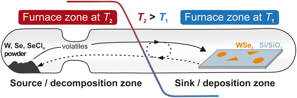 | ||
| Fig. 1 Concept of the experimental work-up of the CVT experiment using a two-chamber silica glass ampoule. Starting materials are placed on the source side (T2) and the SiO2@Si(100) substrate is positioned on the sink side (T1), with T2 > T1. An applied temperature gradient is given as the red line. | ||
Chemical vapor transport experiments
CVT experiments were conducted using a horizontally mounted LOBA two-zoned Tube Furnace (HTM Reetz). For a quantitative transport, the mixture for the bulk synthesis was thermally treated from 900 °C to 820 °C with a heating rate of β = 10 K min−1 towards the temperature gradient targeted and a dwell time of tdwell = 72 h. Subsequently, the ampoules were quenched with water. Nanostructures were synthesized from 850 °C to 800 °C with a heating rate of β = 10 K min−1 towards the temperature gradient aimed and an applied dwell time of tdwell = 60 min. Consequently, ampoules were first cooled on the source side in order to avoid contamination of the crystals grown and stored in the glovebox. Upon cooling in air or quenching with water, crystals appeared in a similar shape which leads to the assumption that quenching has no effect on the result.Characterization of the as-grown crystals
Results and discussion
Rational design of crystal growth by modelling of CVT
Thermodynamic modelling was used as a tool to render ‘trial and error’ approaches for the W/Se/Cl system with a tightened temperature window for essential CVT parameters, such as temperature and the temperature gradient. For this, TRAGMIN simulations allowed bridging theoretical considerations through modelling with experimental methods by chemical vapor precipitation. Based on considerations regarding the ternary phase diagram W/Se/Cl and respective stationary simulations of complex equilibria, the conditions for the endothermic CVT with respect to the temperature and temperature gradient as well as the reaction system composition were chosen to be in the range 800 °C ≤ ϑ ≤ 850 °C (ESI†). Additionally, small excess of selenium species is essential in order to enhance the activity of Se(g) during the crystal growth process that can be realized by the addition of SeCl4(s). Here, SeCl4(s) is the initial experimental addition, while the actual active species and thus also the transport agent are formed in subsequent equilibria. The gaseous species WCl4(s), Se2(g) and SeCl2(g) then become relevant for the transport, while the formation of HCl(g) results from the assumption of experimental conditions that cannot completely avoid the presence of traces of water or moisture. Other oxygen-containing species, such as SeO(g), SeO2(g), and WO2(g) are non-effective in a realistic experimental scenario (pi < 10−26 bar), see Fig. 2. That is, no oxidic contamination should be precipitated at the crystallization site. Finally, a formal dominating transport equation concludes eqn (1).| WSe2(s) + 2SeCl2(g) ⇌ WCl4(g) + 2Se2(g) | (1) |
 | ||
| Fig. 2 Simulation of the partial pressure behavior in a sealed ampoule. (a) Partial pressure for different gas species in the temperature range of 800 °C ≤ ϑ ≤ 850 °C for an endothermic CVT. Area for log(pi) > −4 is marked grey. Non-effective pressure area for p ≤ 10−5 bar is marked red with species shown as the dashed line. Condensed phases shown as the dark grey rectangle. (b) Calculated transport efficiency ωt(i) for the temperature range given. ωt,rel(Se2) corresponds to the homogeneous equilibria in the gas phase for Sew species. | ||
An allocation of essential parameters for the evaluation of the CVT experiments is given by Table 1.
| Material | Modell | n(i)/mmol | ϑ source/°C | ϑ sink/°C | ΔT/K | ṁ calc./mg h−1 | Boundary phases | ||
|---|---|---|---|---|---|---|---|---|---|
| W | Sea | Cl | |||||||
| a Excess for two-room modelling related to addition of SeCl4(s). | |||||||||
| Bulk | Two room | 1 | 2.001 | 0.002 | 1900 | 820 | 80 | 3.36 | — |
| Nano | Two room | 1 | 2.001 | 0.004 | 1915 | 860 | 55 | 1.63 | — |
| Nano | Two room | 1 | 2.001 | 0.004 | 1890 | 840 | 50 | 1.61 | — |
| Nano | Two room | 1 | 2.001 | 0.004 | 1850 | 800 | 50 | 2.15 | — |
Synthesis and characterization of bulk-WSe2
The CVT process for the bulk material was conducted based on the modelling data acquired by TRAGMIN to achieve WSe2 crystals that serve as the reference material (ESI†). Optimized synthesis parameters correspond to the quantitative transport from 900 °C to 820 °C. Bulk-WSe2 crystals show predominantly a hexagonal shape. Crystals occur in slightly varying size, see Fig. 3(a) and (b). Smaller particles on the bulk-WSe2 crystals can derive from broken larger crystals during the sample preparation. SEM images underline the variety in the crystal shape, see Fig. 3(c)–(e). pXRD analysis gives a strong hint for phase purity of the pre-synthesized WSe2, see Fig. 3(f). Reflexes that appear within the diffraction angle range 10° ≤ 2θ ≤ 120° can all be attributed to the 2H modification. The main reflex at 36.6° (2θ) is associated with the preferred (100) orientation. All other reflexes in the diffractogram are in accordance with hexagonal primitive 2H-WSe2 (ICSD: 40752, space group: P63/mmc).42 Complementary to pXRD, EDX analyses reveal a stoichiometric ratio of the elements of W:Se = 1:2, see Fig. 3(g).
 | ||
| Fig. 3 Bulk-WSe2 crystals synthesized by CVT. (a) and (b) Light microscopy images from the as-grown crystals on the sink side of the ampoule and of selected crystals showing a shiny surface. (c)–(e) SEM images showing flat, hexagonally shaped WSe2 crystals. (f) pXRD pattern of bulk-WSe2 within the diffraction angle range 10° ≤ 2θ ≤ 120°, λ(Co Kα1) = 1.788965 Å. Measured in transmission mode. WSe2 reference based on the ICSD database. (g) EDX analysis indicating an elemental ratio of W:Se = 1:2. | ||
Synthesis and characterization of crystals with screw dislocations
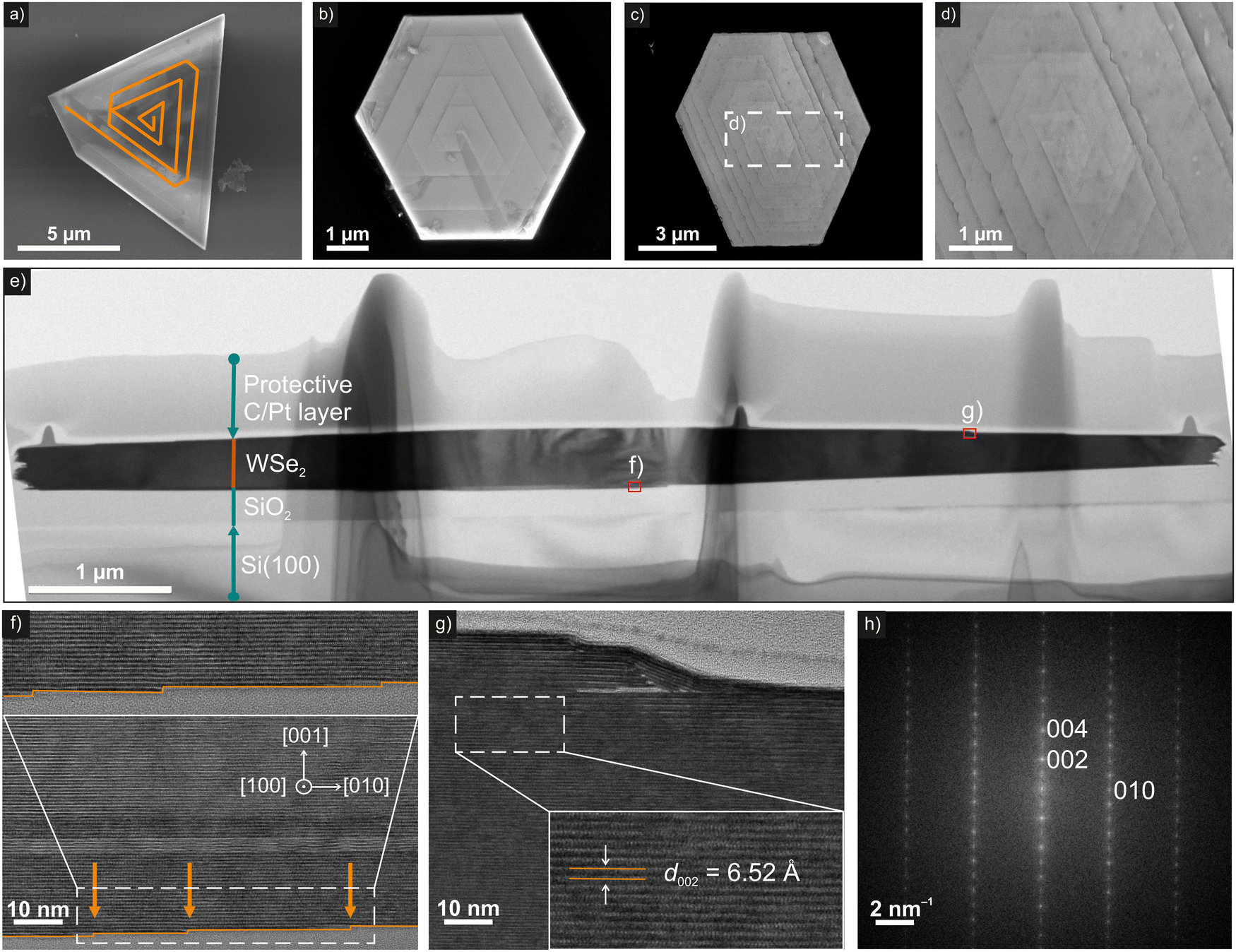 | ||
| Fig. 4 Surface morphology and atomic structure analysis for as-grown WSe2 with screw dislocations using SEM and TEM. (a)–(d) SEM images of triangular and hexagonal WSe2 grown on an SiO2@Si(100) substrate. Screw dislocation-driven growth is redrawn for the triangular crystal. (e) FIB cut of the hexagonally shaped WSe2 crystal (c) with areas selected for high-resolution TEM highlighted. (f) and (g) Cross-sectional high-resolution TEM images of the back (f) and frontside (g) reveal individual steps of the fabricated FIB lamella of the crystals demonstrating a continuous 2H-phase over a larger area. Individual steps are highlighted in orange and depicted enlarged in the inset of (f). (h) Fourier transform (FT) of the area shown in (g). | ||
An important question associated with the pyramidal growth is how the crystal orientation is affected at the screw dislocation zones. Subsequently, EBSD was applied to initially analyze the as-grown WSe2 on the substrate without time-consuming sample preparation. Experimental data were fit with theoretical structure parameters from both the 2H and 1T-bulk reference. Hence, Kikuchi lines were indexed, see Fig. 5. Generally, the EBSD pattern fits with both modifications. However, in the case of 1T-WSe2 it appears that some few of the simulated Kikuchi bands do not fit the observed lines. Thus, EBSD suggests a better fit with the 2H structure type. Considering the bulk synthesis under similar growth conditions, the fitting provides a complementary identification to the pXRD data. This can be taken qualitatively to indicate good crystallinity. Interestingly, further characterization revealed an observable pattern shift along the horizontal as well as the vertical orientations across the sample (ESI†). This orientation change indicates a convex curvature of the sample morphology. The pattern shifts measured at the [001] zone axis via cross correlation result in a horizontal pattern shift of Sx = (0.362 ± 0.039) mm. With respect to the pattern on the top and bottom of the sample, the vertical pattern shift of Sy = (0.626 ± 0.024) mm is noteworthily larger than along the horizontal and thus corresponds to a convex curvature. The curvature radii were determined as Rx = (270 ± 32) μm and Ry = (141 ± 9) μm, respectively. Any orientation change can be induced either by plastic deformation via dislocations or by elastic strain/strain relaxation at boundaries.45
 | ||
| Fig. 5 EBSD characterization for as-grown 2H-WSe2 with screw dislocations with simulated Kikuchi lines and indexed zone axes. | ||
 | (2) |
 | ||
| Fig. 6 AFM measurements of three representative nm-scale WSe2 crystals with a right-handed spiral stacking topology. Depicted green measurement lines correspond to the respective height profiles below. For further characterization each height and terrace width were measured. Each step is indexed. | ||
The terrace widths vary from 637 nm at smallest to 711 nm at largest for the crystal shown in Fig. 6(c) and (d). Consequently, the slope for each step varies in the range 0.0145 ≤ s ≤ 0.0180. The average slope for the WSe2 crystal is 0.0156 and is similar to the slope of 0.0126 reported by Chen et al.56
The majority of the features can be categorized into small steps and slopes as well as general low supersaturation condition per definition, see Fig. 7(a). Indeed, our data suggest that growth conditions are linked sufficiently accurate to low supersaturation. All examined height profiles indicate that WSe2 was grown under conditions of low supersaturation.
 | ||
| Fig. 7 (a) Surface morphology characteristics of several WSe2 crystals with screw dislocations. All heights and terrace widths were determined by AFM height profiles. Grey arrows indicate general growth conditions and related crystal features. Features marked by the dashed rectangle represent edge-close steps on the crystal. (b) Dependency of average terrace width from calculated temperature-dependent equilibrium constant Kp for each synthesis temperature regime. | ||
Additional TRAGMIN modelling and CVT experiments performed in the predicted temperature range from 800 °C to 950 °C revealed comparable vapor pressure characteristics and thus similar growth. Indeed, WSe2 crystals show step heights that correlate with smaller slopes at elevated temperatures. Differences in step heights and slopes should be linked to varying deposition temperatures and temperature gradients, whereas calculated transport rates are similar (915 °C → 860 °C: ṁcalc. = 1.63 mg h−1vs. 890 °C → 840 °C: ṁcalc. = 1.61 mg h−1). Crystals grown at 860 °C exhibit small slopes (w < 400 nm) and low step heights (h < 5 nm). Lower deposition temperatures indicate broader terrace widths (w > 500 nm) with height steps of around 10 nm. Crystals with a pyramid-like topography (ϑsink = 800 °C) correlate with small steps and terrace widths, which results in narrowly arranged surface characteristics.
A semi-quantitative approach to further link theoretical considerations and the CVT experiments is to plot the difference of the respective equilibrium constant ΔKp, i.e., Kp(T2) − Kp(T1), for the dominant transport equilibrium eqn (1) from T2 → T1, with T2 > T1, against the terrace width of the crystals. Hereby, ΔKp is a representative for the growth conditions chosen. The data for the average terrace width for each synthesis condition give a strong hint for a linear trend, see Fig. 7(b). Thereby, TRAGMIN simulations is a tool to predict a tightened temperature window for controlled growth of crystals with screw dislocations and to fine-tune the characteristic features of the crystals.
 | ||
| Fig. 8 (a) Raman spectra of pre-synthesized bulk-WSe2, and nm-scale WSe2 crystals excited with depolarized lasers at 660 nm and 532 nm. (b) Polarized spectra of bulk and nano-WSe2 excited at 660 nm and measured with step-wise rotation of the laser polarization plane with respect to the crystal and polarization direction of the detector (angles of 0° and 90° correspond to xx and xy polarization geometries). (c) Polarized spectra of bulk and nano-WSe2 excited at 532 nm with two polarization geometries, parallel (xx) and cross-polarized (xy). In each panel, insets show the range of 226 cm−1 ≤ ṽ ≤ 274 cm−1, depicted enlarged for better comparison of the most prominent features. Additional inset in (c) compares the range of low-frequency shear mode (E22g) of bulk and nano-WSe2 measured in the cross-polarized geometry. | ||
When studied in back-scattering geometry with the laser beam perpendicular to the basal plane, WSe2 in the D6h factor group has only three first-order Raman-active vibrations at the Γ-point, one out-of-plane A1g and two in-plane 2 E2g modes. Experimental spectra of WSe2 are usually dominated by nearly-degenerate E12g and A1g peaks at 247 cm−1 and 250 cm−1, accompanied by a broader band at ≈260 cm−1 associated with the two-phonon 2 LA(M) feature. In fact, the latter band has an asymmetric shape with 2–3 unresolved components, whose assignment is not completely clear yet. For instance, in ref. 60, the feature at 256 cm−1 was ascribed to the B2g(M) mode, while the 2 LA(M) proper identified at 260 cm−1, an assignment for the shoulder at 263 cm−1 to A(M) mode as was proposed in ref. 57. As the 220–280 cm−1 range has the highest Raman activity and narrow spacing of the peaks, we plot it enlarged in insets of Fig. 8. Aside from the first-order phonons, Raman spectra of WSe2 are rich with a number of second-order features, whose relative intensity depends on the excitation wavelength and is stronger for the resonant excitation at 532 nm. A tentative assignment for prominent second-order peaks and formally inactive modes is given in Fig. 8(a) and supplement based on the data from ref. 57 and 60–64.
All Raman modes detected for the bulk-WSe2 reference were also ascribed for the nm-scale crystals. Second-order features are observed for the latter with similar relative intensities and, within accuracy limits of 0.1–0.2 cm−1, at the same peak positions as for the bulk WSe2. However, there are also certain differences between the spectra, particularly visible in the 220–280 cm−1 range encompassing E12g, A1g, and 2 LA(M) modes. Under the 660 nm excitation, A1g has considerably higher intensity than E12g both in bulk and nm-scale crystals. The main difference between the samples is in the 2 LA(M) band, which in the bulk-WSe2 has lower relative intensity but a better-defined shape with two features at 256 cm−1 and 261 cm−1. In the nano-WSe2, the 2 LA(M) band has higher intensity, but the peak shape is more asymmetric and encompasses at least three unresolved features at 255, 256, and 261 cm−1. Under the 532 nm excitation, the intensity ratio of the E12g/A1g peak changes considerably when compared to that of the spectra obtained with the 660 nm laser. In the bulk-WSe2, only the E12g peak is clearly visible, while A1g is much weaker than E12g and the 2 LA(M) bands and cannot be resolved. The nano-WSe2 exhibits quite a different pattern in that A1g is only slightly weaker than E12g and is clearly visible, while intensity of the 2 LA(M) band is reduced considerably relative to the E12g/A1g pair.
To confirm symmetry assignments and to find if crystals with screw dislocations have different angular dependence of polarization, we performed polarized Raman measurements. Fig. 8(b) shows the spectra of bulk and nano-WSe2 obtained by rotation of the 660 nm laser polarization in 10° steps, from the parallel orientation of the laser and analyzer (0°, xx) to the cross-polarized geometry (90°, xy). For D6h symmetry and propagation of incident and scattered light along the z-axis, A1g modes are active in xx and forbidden in xy orientations, while intensity of E2g mode should not depend on the angle. In accordance with symmetry, we do observe a strong modulation of the A1g peak from the full-scale at 0° to zero at 90°, whereas the E2g peak remains nearly constant. The angular dependence is identical for bulk and nano-WSe2, showing that the screw dislocation does not affect the local symmetry. Similarly, xx and xy-polarized measurements with the 532 nm excitation confirmed assignments of A1g and E2g modes and their regular polarization dependence (Fig. 8(c)). For the bulk sample, a weak signal of the A1g mode became visible in the xx polarization, while enhanced intensity of the A1g mode in the nano-WSe2 is further corroborated in the xx-polarized spectrum.
Low-frequency interlayer modes can be particularly interesting for the analysis of the morphological aspects in 2D materials as they are sensitive to the interlayer stacking geometry and interactions. While interlayer breathing mode of bulk-WSe2 has B22g symmetry and is optically silent, the shear mode with E22g symmetry, in which layers are displaced in the antiparallel direction, is Raman active and occurs near 25 cm−1.61
Although the low intensity and overlap with the strong Rayleigh background of the laser precluded detection of the E22g mode under 660 nm excitation, a sharp and very strong peak at 24.6 cm−1 was observed for the bulk sample excited with the 532 nm laser (Fig. 8(a)). The peak has similar intensity in xx and xy polarization geometries, confirming its assignment to the E2g symmetry. For the nano-WSe2 sample, we could not reliably detect the shear mode in non-polarized or xx-polarized spectra because of the strong laser tail, but suppression of the Rayleigh background in the xy polarization allowed a detection of the weaker signal at 22.2 cm−1 (Fig. 8(c)). The E22g mode intensity in nano-WSe2 is three times smaller than the intensity of the E12g mode, while in the bulk-WSe2 the shear mode is stronger than E12g by a factor of 2.5. The frequency shift of 2.4 cm−1 between the bulk and nano-WSe2 is also quite characteristic and is in line with the earlier report by Shearer et al.,48 who found that the crystals with a hexagonal spiral dislocation had the shear mode at the same frequency as in bulk-WSe2, and crystals with a triangular dislocation did not show a shear mode at all, while mixed hexagonal-triangular crystals exhibited a downshift by 3 cm−1.
Chirality of the crystals with screw dislocations suggests that they should show an optical activity,65–67 which we addressed by circularly polarized (CP) Raman spectroscopy.68 According to the selection rules for CP-Raman, A1g mode of WSe2 is active when both incident and scattered lights have the same helicity (σ+σ+ and σ−σ− configurations), whereas the E2g mode is active for opposite polarizations of the incident and scattered lights (σ+σ− and σ−σ+ configurations).69 Indeed, CP-Raman spectra of bulk and nano-WSe2 samples demonstrate mutually exclusive activity of E12g and A1g modes (Fig. 9). For the achiral bulk-WSe2, E12g mode has the same intensity in the σ+σ− and σ−σ+ spectra. However, in the crystals with screw dislocations (Fig. 9a and b), σ+σ− and σ−σ+ intensities of the E12g peak are noticeably different. The σ+σ− intensity exceeds the σ−σ+ intensity in the right-handed crystal by 29%, whereas in the left-handed crystal the σ−σ+ peak is higher than the σ+σ− peak by 15%. The less pronounced Raman optical activity of the left-handed crystal is presumably caused by the larger size of the terraces. Interestingly, the vast majority of synthesized nano-crystals appeared to be right-handed, whereas left-handed crystals were only observed from 915 °C → 860 °C. We studied one of the crystals in different places and did not find a considerable variation of the polarization (ESI†). Based on the identical substrate preparation but different deposition temperatures for right and left-handed spirals, we assume the sink temperature to be the main factor to affect the growth, and thus the temperature ranges can serve as selectivity criteria to differentiate between the two types of WSe2 spirals by CVT.
 | ||
| Fig. 9 (a) and (b) SEM images of WSe2 crystals with screw dislocations and opposite chiralities: (a) left-handed, nano-WSe2-L, (b) right-handed, nano-WSe2-R. (c) Circular-polarized Raman spectra of bulk-WSe2 and crystals with screw dislocations, whose SEM images are shown in (a) and (b). Spectra were excited with a 532 nm laser. | ||
To summarize, while demonstrating a similarity in the overall vibrational pattern, Raman measurements also revealed clear distinctions between bulk-WSe2 and nano-WSe2 crystals with screw dislocations. The most pronounced differences are in the intensity and frequency of the interlayer shear mode, and in the relative intensities of E12g, A1g, and 2 LA(M) modes. While the former points to the changes in the interlayer interactions, the latter highlights the alterations in the Raman resonance conditions and can therefore evidence the variation in the electronic structure of WSe2.
Conclusion
In summary, triangular and hexagonal pyramid-like WSe2 nano-scale crystals with screw dislocations were synthesized by custom-designed CVT experiments based on a rational synthesis approach applying thermodynamic modelling. The simulations allowed designing a temperature range for optimized growth conditions during the CVT process. Vibrational spectroscopy using Raman revealed all modes detected for bulk and nano-WSe2 were found with similar peak intensities and positions with main differences including both the intensity ratio of the E12g/A1g peak changed significantly and the 2 LA(M) band characterized with a more asymmetric shape for nano-WSe2. The screw dislocation was found to have no effect on the local symmetry according to the angular dependence. Right and left-handed spiral stackings affected the intensity of the E12g mode by 29% and 15%, respectively. With EBSD, we were able to elucidate the high crystallinity of the as-grown WSe2 directly on the substrate, index Kikuchi lines and link it to the 2H modification. The EBSD patterns indicate a gradual orientation change across the sample which corresponds to a convex curvature. We determined the horizontal and vertical pattern shifts and calculated the respective curvature radii, with the curvature radius along the horizontal orientation found to be significantly larger. Key features of the screw dislocation were found to be a step height of around 10 nm with the respective terrace widths varying depending on the modelled temperature ranges. In addition, characteristics are linked to theoretical considerations. Thereby, the terrace widths correlate linearly with the supersaturation conditions during the crystal growth, which is represented by the temperature-dependent equilibrium constant. Connecting thermodynamic considerations with actual CVT experiments enabled determining the optimum reaction conditions for the low supersaturation and thus opens up a pathway for further rational design of screw dislocation-driven growth by CVT.Author contributions
P. S., S. H. and B. B. conceived and designed the project. P. P. conducted the synthesis of materials, thermodynamic modelling and analysis, optical microscopy/SEM, AFM and pXRD characterization and analysis. D. W. performed the HR-TEM measurements. A. A. P. contributed to the Raman analysis. J. G. and T. R. carried out the EBSD measurements. P. C. and T. R. carried out the EBSD analysis. The manuscript was written by P. P. based on contributions from all authors. S. H. and B. B. were responsible for the project management.Data availability
The data supporting this article have been included in the ESI.†Conflicts of interest
There are no conflicts to declare.Acknowledgements
P. P. and S. H. acknowledge funding from the IFW Excellence Program 2022 of the Leibniz Institute for Solid State and Materials Research. D. W. received funding from the “Deutsche Forschungsgemeinschaft” with project number 417590517 and grant number SFB 1415. The authors thank Robert Heider for laboratory support. We thank Almut Pöhl for the preparation of the FIB lamella of WSe2 for the HR-TEM measurements, Prof. Ellen Hieckmann for the EBSD measurements and Sandra Schiemenz for the Raman measurements.References
- K. S. Novoselov, A. K. Geim, S. V. Morozov, D. Jiang, Y. Zhang, S. V. Dubonos, I. V. Grigorieva and A. A. Firsov, Electric Field Effect in Atomically Thin Carbon Films, Science, 2004, 306(5696), 666–669, DOI:10.1126/science.1102896.
- K. S. Novoselov, A. Mishchenko, A. Carvalho and A. H. Castro Neto, 2D Materials and van der Waals Heterostructures, Science, 2016, 353(6298), aac9439, DOI:10.1126/science.aac9439.
- Y. Liu, Y. Huang and X. Duan, van der Waals Integration before and beyond Two-Dimensional Materials, Nature, 2019, 567(7748), 323–333, DOI:10.1038/s41586-019-1013-x.
- S. J. McDonnell and R. M. Wallace, Atomically-Thin Layered Films for Device Applications Based upon 2D TMDC Materials, Thin Solid Films, 2016, 616, 482–501, DOI:10.1016/j.tsf.2016.08.068.
- H. Zhang, L.-M. Liu and W.-M. Lau, Dimension-Dependent Phase Transition and Magnetic Properties of VS2, J. Mater. Chem. A, 2013, 1(36), 10821–10828, 10.1039/C3TA12098H.
- G. Fiori, F. Bonaccorso, G. Iannaccone, T. Palacios, D. Neumaier, A. Seabaugh, S. K. Banerjee and L. Colombo, Electronics Based on Two-Dimensional Materials, Nat. Nanotechnol., 2014, 9(10), 768–779, DOI:10.1038/nnano.2014.207.
- F. H. L. Koppens, T. Mueller, P. Avouris, A. C. Ferrari, M. S. Vitiello and M. Polini, Photodetectors Based on Graphene, Other Two-Dimensional Materials and Hybrid Systems, Nat. Nanotechnol., 2014, 9(10), 780–793, DOI:10.1038/nnano.2014.215.
- W.-X. Zhou and K.-Q. Chen, First-Principles Determination of Ultralow Thermal Conductivity of Monolayer WSe2, Sci. Rep., 2015, 5(1), 15070, DOI:10.1038/srep15070.
- N. Kumari, M. Kalyan, S. Ghosh, A. R. Maity and R. Mukherjee, Possible Negative Correlation between Electrical and Thermal Conductivity in P-Doped WSe2 Single Crystal, Mater. Res. Express, 2021, 8(4), 045902, DOI:10.1088/2053-1591/abf682.
- K. K. Kam and B. A. Parkinson, Detailed Photocurrent Spectroscopy of the Semiconducting Group VIB Transition Metal Dichalcogenides, J. Phys. Chem., 1982, 86(4), 463–467, DOI:10.1021/j100393a010.
- S. A. Han, R. Bhatia and S.-W. Kim, Synthesis, Properties and Potential Applications of Two-Dimensional Transition Metal Dichalcogenides, Nano Converge., 2015, 2(1), 1–14, DOI:10.1186/s40580-015-0048-4.
- R. Murray and B. Evans, The Thermal Expansion of 2H-MoS2 and 2H-WSe2 between 10 and 320 K, J. Appl. Crystallogr., 1979, 12(3), 312–315, DOI:10.1107/S0021889879012528.
- Y. J. Park, H.-S. So, H. Hwang, D. S. Jeong, H. J. Lee, J. Lim, C. G. Kim and H. S. Shin, Synthesis of 1T WSe2 on an Oxygen-Containing Substrate Using a Single Precursor, ACS Nano, 2022, 16(7), 11059–11065, DOI:10.1021/acsnano.2c03762.
- E. Y. Andrei, D. K. Efetov, P. Jarillo-Herrero, A. H. MacDonald, K. F. Mak, T. Senthil, E. Tutuc, A. Yazdani and A. F. Young, The Marvels of Moiré Materials, Nat. Rev. Mater., 2021, 6(3), 201–206, DOI:10.1038/s41578-021-00284-1.
- Y. Cao, V. Fatemi, S. Fang, K. Watanabe, T. Taniguchi, E. Kaxiras and P. Jarillo-Herrero, Unconventional Superconductivity in Magic-Angle Graphene Superlattices, Nature, 2018, 556(7699), 43–50, DOI:10.1038/nature26160.
- G. Chen, L. Jiang, S. Wu, B. Lyu, H. Li, B. L. Chittari, K. Watanabe, T. Taniguchi, Z. Shi, J. Jung, Y. Zhang and F. Wang, Evidence of a Gate-Tunable Mott Insulator in a Trilayer Graphene Moiré Superlattice, Nat. Phys., 2019, 15(3), 237–241, DOI:10.1038/s41567-018-0387-2.
- K. L. Seyler, P. Rivera, H. Yu, N. P. Wilson, E. L. Ray, D. G. Mandrus, J. Yan, W. Yao and X. Xu, Signatures of Moiré-Trapped Valley Excitons in MoSe2/WSe2 Heterobilayers, Nature, 2019, 567(7746), 66–70, DOI:10.1038/s41586-019-0957-1.
- K. Tran, G. Moody, F. Wu, X. Lu, J. Choi, K. Kim, A. Rai, D. A. Sanchez, J. Quan and A. Singh, Evidence for Moiré Excitons in van der Waals Heterostructures, Nature, 2019, 567(7746), 71–75, DOI:10.1038/s41586-019-0975-z.
- Q. Xu, Y. Guo and L. Xian, Moiré Flat Bands in Twisted 2D Hexagonal VdW Materials, 2D Mater., 2021, 9(1), 14005, DOI:10.1088/2053-1583/ac3a98.
- S. A. Morin, M. J. Bierman, J. Tong and S. Jin, Mechanism and Kinetics of Spontaneous Nanotube Growth Driven by Screw Dislocations, Science, 2010, 328(5977), 476–480, DOI:10.1126/science.1182977.
- Y. Sun, Y. Jiang, J. Jiang, T. Li and M. Liu, Keto-Form Directed Hierarchical Chiral Self-Assembly of Schiff Base Derivatives with Amplified Circularly Polarized Luminescence, Chin. Chem. Lett., 2024, 35(1), 108409, DOI:10.1016/j.cclet.2023.108409.
- J. Yeom, B. Yeom, H. Chan, K. W. Smith, S. Dominguez-Medina, J. H. Bahng, G. Zhao, W.-S. Chang, S.-J. Chang, A. Chuvilin, D. Melnikau, A. L. Rogach, P. Zhang, S. Link, P. Král and N. A. Kotov, Chiral Templating of Self-Assembling Nanostructures by Circularly Polarized Light, Nat. Mater., 2015, 14(1), 66–72, DOI:10.1038/nmat4125.
- T. D. James, K. R. A. Samankumara Sandanayake and S. Shinkai, Chiral Discrimination of Monosaccharides Using a Fluorescent Molecular Sensor, Nature, 1995, 374(6520), 345–347, DOI:10.1038/374345a0.
- M. Bartók, Unexpected Inversions in Asymmetric Reactions: Reactions with Chiral Metal Complexes, Chiral Organocatalysts, and Heterogeneous Chiral Catalysts, Chem. Rev., 2010, 110(3), 1663–1705, DOI:10.1021/cr9002352.
- R. Naaman and D. H. Waldeck, Spintronics and Chirality: Spin Selectivity in Electron Transport Through Chiral Molecules, Annu. Rev. Phys. Chem., 2015, 66(1), 263–281, DOI:10.1146/annurev-physchem-040214-121554.
- R. Tanuma, I. Kamata, J. P. Hadorn and H. Tsuchida, Two-Photon-Excited, Three-Dimensional Photoluminescence Imaging and Dislocation-Line Analysis of Threading Dislocations in 4H-SiC, J. Appl. Phys., 2018, 124(12), 125703, DOI:10.1063/1.5043238.
- D.-B. Zhang, T. Dumitrică and G. Seifert, Helical Nanotube Structures of MoSe2 with Intrinsic Twisting: An Objective Molecular Dynamics Study, Phys. Rev. Lett., 2010, 104(6), 065502, DOI:10.1103/PhysRevLett.104.065502.
- J. Ai, Y. Wang, L. Li, J. Wang, T. Bai, S. Che and L. Han, Determination of Multilevel Chirality in Nickel Molybdate Films by Electron Crystallography, Nano Res., 2024, 17(9), 8571–8577, DOI:10.1007/s12274-024-6865-1.
- B. Sung, A. de la Cotte and E. Grelet, Chirality-Controlled Crystallization via Screw Dislocations, Nat. Commun., 2018, 9(1), 1405, DOI:10.1038/s41467-018-03745-4.
- T. Verbiest, S. Van Elshocht, M. Kauranen, L. Hellemans, J. Snauwaert, C. Nuckolls, T. J. Katz and A. Persoons, Strong Enhancement of Nonlinear Optical Properties Through Supramolecular Chirality, Science, 1998, 282(5390), 913–915, DOI:10.1126/science.282.5390.913.
- R. Naaman, Y. Paltiel and D. H. Waldeck, Chiral Molecules and the Electron Spin, Nat. Rev. Chem., 2019, 3(4), 250–260, DOI:10.1038/s41570-019-0087-1.
- G. Chang, B. J. Wieder, F. Schindler, D. S. Sanchez, I. Belopolski, S.-M. Huang, B. Singh, D. Wu, T.-R. Chang, T. Neupert, S.-Y. Xu, H. Lin and M. Z. Hasan, Topological Quantum Properties of Chiral Crystals, Nat. Mater., 2018, 17(11), 978–985, DOI:10.1038/s41563-018-0169-3.
- J. B. Legma, G. Vacquier and A. Casalot, Chemical Vapour Transport of Molybdenum and Tungsten Diselenides by Various Transport Agents, J. Cryst. Growth, 1993, 130(1–2), 253–258, DOI:10.1016/0022-0248(93)90859-U.
- A. A. Al-Hilli and B. L. Evans, The Preparation and Properties of Transition Metal Dichalcogenide Single Crystals, J. Cryst. Growth, 1972, 15(2), 93–101, DOI:10.1016/0022-0248(72)90129-7.
- R. Kershaw, M. Vlasse and A. Wold, The Preparation of and Electrical Properties of Niobium Selenide and Tungsten Selenide, Inorg. Chem., 1967, 6(8), 1599–1602, DOI:10.1021/ic50054a043.
- M. Bougouma, B. Nisol, T. Doneux, B. Guel, T. Segato, F. Reniers, M.-P. Delplancke-Ogletree, J. B. Legma and C. Buess-Herman, Growth and Characterization of WSe2 Single Crystals Using TeCl4 as Transport Agent, J. Cryst. Growth, 2016, 453, 111–118, DOI:10.1016/j.jcrysgro.2016.08.025.
- N. D. Boscher, C. J. Carmalt and I. P. Parkin, Atmospheric Pressure Chemical Vapor Deposition of WSe2 Thin Films on Glass—Highly Hydrophobic Sticky Surfaces, J. Mater. Chem., 2006, 16(1), 122–127, 10.1039/B514440J.
- L. Chen, B. Liu, A. N. Abbas, Y. Ma, X. Fang, Y. Liu and C. Zhou, Screw-Dislocation-Driven Growth of Two-Dimensional Few-Layer and Pyramid-like WSe2 by Sulfur-Assisted Chemical Vapor Deposition, ACS Nano, 2014, 8(11), 11543–11551, DOI:10.1021/nn504775f.
- X. Wang, Y. Li, L. Zhuo, J. Zheng, X. Peng, Z. Jiao, X. Xiong, J. Han and W. Xiao, Controllable Growth of Two-Dimensional WSe2 Using Salt as Co-Solvent, CrystEngComm, 2018, 20(40), 6267–6272, 10.1039/C8CE01162A.
- F. Hansen, M. Wels, S. Froeschke, A. Popov, D. Wolf, B. Büchner, P. Schmidt and S. Hampel, Thermodynamic Evaluation and Chemical Vapor Transport of Few-Layer WTe2, Cryst. Growth Des., 2020, 20(11), 7341–7349, DOI:10.1021/acs.cgd.0c01004.
- G. Krabbes, W. Bieger, K.-H. Sommer, T. Söhnel and U. Steiner, GMIN Version 5.2: Package TRAGMIN for Calculation of Thermodynamic Equilibrium, Dresden, 2014, https://www.htw-dresden.de/luc/forschung/chemieingenieurwesen/festkoerperchemie/tragmin Search PubMed.
- W. J. Schutte, J. L. De Boer and F. Jellinek, Crystal Structures of Tungsten Disulfide and Diselenide, J. Solid State Chem., 1987, 70(2), 207–209, DOI:10.1016/0022-4596(87)90057-0.
- Y. Zhao and S. Jin, Stacking and Twisting of Layered Materials Enabled by Screw Dislocations and Non-Euclidean Surfaces, Acc. Mater. Res., 2022, 3(3), 369–378, DOI:10.1021/accountsmr.1c00245.
- Y. Zhao, C. Zhang, D. D. Kohler, J. M. Scheeler, J. C. Wright, P. M. Voyles and S. Jin, Supertwisted Spirals of Layered Materials Enabled by Growth on Non-Euclidean Surfaces, Science, 2020, 370(6515), 442–445, DOI:10.1126/science.abc4284.
- P. Haasen, Physikalische Metallkunde, Springer, Berlin, 3rd edn, 2013, p. 255 Search PubMed.
- S. A. Morin, A. Forticaux, M. J. Bierman and S. Jin, Screw Dislocation-Driven Growth of Two-Dimensional Nanoplates, Nano Lett., 2011, 11(10), 4449–4455, DOI:10.1021/nl202689m.
- A. Zhuang, J. Li, Y. Wang, X. Wen, Y. Lin, B. Xiang, X. Wang and J. Zeng, Screw-Dislocation-Driven Bidirectional Spiral Growth of Bi2Se3 Nanoplates, Angew. Chem., Int. Ed., 2014, 53(25), 6425–6429, DOI:10.1002/anie.201403530.
- M. J. Shearer, L. Samad, Y. Zhang, Y. Zhao, A. Puretzky, K. W. Eliceiri, J. C. Wright, R. J. Hamers and S. Jin, Complex and Noncentrosymmetric Stacking of Layered Metal Dichalcogenide Materials Created by Screw Dislocations, J. Am. Chem. Soc., 2017, 139(9), 3496–3504, DOI:10.1021/jacs.6b12559.
- M. C. C. Giacovazzo, H. L. Monaco, G. Artioli, D. Viterbo, G. Ferraris, G. Gilli and G. Zanotti, Fundamentals of Crystallography, Oxford University Press, Oxford, 2nd edn, 2002 Search PubMed.
- J. Dong, L. Zhang and F. Ding, Kinetics of Graphene and 2D Materials Growth, Adv. Mater., 2019, 31(9), 1801583, DOI:10.1002/adma.201801583.
- M. J. Greenberg, Euclidean and Non-Euclidean Geometries: Development and History, W.H. Freeman and Company, New York, 4th edn, 2007 Search PubMed.
- M. J. Bierman, Y. K. A. Lau, A. V. Kvit, A. L. Schmitt and S. Jin, Dislocation-Driven Nanowire Growth and Eshelby Twist, Science, 2008, 320(5879), 1060–1063, DOI:10.1126/science.1157131.
- T. Tong, R. Chen, Y. Ke, Q. Wang, X. Wang, Q. Sun, J. Chen, Z. Gu, Y. Yu, H. Wei, Y. Hao, X. Fan and Q. Zhang, Giant Second Harmonic Generation in Supertwisted WS2 Spirals Grown in Step-Edge Particle-Induced Non-Euclidean Surfaces, ACS Nano, 2024, 18(33), 21939–21947, DOI:10.1021/acsnano.4c02807.
- R. Y. Tay, H. J. Park, J. Lin, Z. K. Ng, L. Jing, H. Li, M. Zhu, S. H. Tsang, Z. Lee and E. H. T. Teo, Concentric and Spiral Few-Layer Graphene: Growth Driven by Interfacial Nucleation vs. Screw Dislocation, Chem. Mater., 2018, 30(19), 6858–6866, DOI:10.1021/acs.chemmater.8b03024.
- H. J. Park, R. Y. Tay, X. Wang, W. Zhao, J. H. Kim, R. S. Ruoff, F. Ding, E. H. T. Teo and Z. Lee, Double-Spiral Hexagonal Boron Nitride and Shear Strained Coalescence Boundary, Nano Lett., 2019, 19(7), 4229–4236, DOI:10.1021/acs.nanolett.8b05034.
- L. Chen, B. Liu, A. N. Abbas, Y. Ma, X. Fang, Y. Liu and C. Zhou, Screw-Dislocation-Driven Growth of Two-Dimensional Few-Layer and Pyramid-like WSe2 by Sulfur-Assisted Chemical Vapor Deposition, ACS Nano, 2014, 8(11), 11543–11551, DOI:10.1021/nn504775f.
- E. Del Corro, H. Terrones, A. Elias, C. Fantini, S. Feng, M. A. Nguyen, T. E. Mallouk, M. Terrones and M. A. Pimenta, Excited Excitonic States in 1L, 2L, 3L, and Bulk WSe2 Observed by Resonant Raman Spectroscopy, ACS Nano, 2014, 8(9), 9629–9635, DOI:10.1021/nn504088g.
- A. R. Beal, J. C. Knights and W. Y. Liang, Transmission Spectra of Some Transition Metal Dichalcogenides. II. Group VIA: Trigonal Prismatic Coordination, J. Phys. C: Solid State Phys., 1972, 5(24), 3540–3551, DOI:10.1088/0022-3719/5/24/016.
- R. F. Frindt, The Optical Properties of Single Crystals of WSe2 and MoTe2, J. Phys. Chem. Solids, 1963, 24(9), 1107–1108, DOI:10.1016/0022-3697(63)90024-6.
- L. Du, M. Liao, J. Tang, Q. Zhang, H. Yu, R. Yang, K. Watanabe, T. Taniguchi, D. Shi, Q. Zhang and G. Zhang, Strongly Enhanced Exciton-Phonon Coupling in Two-Dimensional WSe2, Phys. Rev. B, 2018, 97(23), 235145, DOI:10.1103/PhysRevB.97.235145.
- D. G. Mead and J. C. Irwin, Long Wavelength Optic Phonons in WSe2, Can. J. Phys., 1977, 55(5), 379–382, DOI:10.1139/p77-052.
- X. Luo, Y. Zhao, J. Zhang, M. Toh, C. Kloc, Q. Xiong and S. Y. Quek, Effects of Lower Symmetry and Dimensionality on Raman Spectra in Two-Dimensional WSe2, Phys. Rev. B: Condens. Matter Mater. Phys., 2013, 88(19), 195313, DOI:10.1103/PhysRevB.88.195313.
- K. Akintola, G. T. Andrews, S. H. Curnoe, M. R. Koehler and V. Keppens, Raman and Brillouin Scattering Studies of Bulk 2H-WSe2, J. Phys.: Condens. Matter, 2015, 27(39), 395401, DOI:10.1088/0953-8984/27/39/395401.
- X. Zhang, Q.-H. Tan, J.-B. Wu, W. Shi and P.-H. Tan, Review on the Raman Spectroscopy of Different Types of Layered Materials, Nanoscale, 2016, 8(12), 6435–6450, 10.1039/C5NR07205K.
- L. Zhang, K. Liu, A. B. Wong, J. Kim, X. Hong, C. Liu, T. Cao, S. G. Louie, F. Wang and P. Yang, Three-Dimensional Spirals of Atomic Layered MoS2, Nano Lett., 2014, 14(11), 6418–6423, DOI:10.1021/nl502961e.
- X. Fan, Y. Jiang, X. Zhuang, H. Liu, T. Xu, W. Zheng, P. Fan, H. Li, X. Wu, X. Zhu, Q. Zhang, H. Zhou, W. Hu, X. Wang, L. Sun, X. Duan and A. Pan, Broken Symmetry Induced Strong Nonlinear Optical Effects in Spiral WS2 Nanosheets, ACS Nano, 2017, 11(5), 4892–4898, DOI:10.1021/acsnano.7b01457.
- P. K. Barman, P. V. Sarma, M. M. Shaijumon and R. N. Kini, High Degree of Circular Polarization in WS2 Spiral Nanostructures Induced by Broken Symmetry, Sci. Rep., 2019, 9(1), 2784, DOI:10.1038/s41598-019-39246-7.
- Y. Zhao, B. Xu, L. Tong and J. Zhang, The Helicity of Raman Scattered Light: Principles and Applications in Two-Dimensional Materials, Sci. China: Chem., 2022, 65(2), 269–283, DOI:10.1007/s11426-021-1119-4.
- S. Kim, K. Kim, J.-U. Lee and H. Cheong, Excitonic Resonance Effects and Davydov Splitting in Circularly Polarized Raman Spectra of Few-Layer WSe2, 2D Mater., 2017, 4(4), 045002, DOI:10.1088/2053-1583/aa8312.
Footnote |
| † Electronic supplementary information (ESI) available: Additional experimental details, SEM and AFM images, the database for the thermodynamic modellings, thermodynamic modellings, a ternary phase diagram, EDX spectra, pXRD data, AFM data, EBSD data, and Raman results (PDF). See DOI: https://doi.org/10.1039/d4nh00567h |
| This journal is © The Royal Society of Chemistry 2025 |