DOI:
10.1039/D5MA00124B
(Paper)
Mater. Adv., 2025,
6, 3280-3292
Black gold layers: preparation via thermal evaporation, material and optical properties, and application potential for gas sensors†
Received
11th February 2025
, Accepted 27th March 2025
First published on 31st March 2025
Abstract
Nanostructured black metal (BM) layers represent a valuable material for many technological applications. Their unique properties resulting from their structure have led to their use as electromagnetic absorbers, gas sensing devices, and electronics. Although black gold films have been extensively studied, there is still a gap in the use of evaporated BM films for sensor applications. This paper compares the material and optical properties of reflective and black gold films, both of which were prepared by applying the thermal evaporation technique in a residual argon atmosphere. The impact of the nanostructured surface is discussed from the perspectives of morphology, chemical composition, emissivity, reflectivity, and absorbance. Microscopic analyses revealed that black gold comprises nanograins aggregated into a cauliflower-like structure. Positron annihilation spectroscopy reported a high concentration of pores in the black gold layer with a mean size of 1.1 nm. This highly porous structure allows high light absorbance in the visible wavelength range and strong electron plasma interactions in the infrared wavelength range. Preliminary results for gas sensing response to NO2, CH3CH2OH, NH3 and CO reveal the promising use of black gold coating for sensor applications.
1. Introduction
Porous metallic layers have attracted significant interest from the scientific community in the past1–4 for their unique properties resulting from their delicate surface structures. In particular, in the field of gas sensing, black metal (BM) layers have shown promising results as they can further enhance the sensing capabilities of such devices.2 Various metal layers, including aluminium, silver, gold, platinum, and palladium, can be prepared in a finely nano-structured form with their surface densely populated with numerous cracks and cavities in the nanoscale.3,5–8 These surface deformities create a cauliflower-like surface structure, allowing incident light to enter and undergo several reflections with a very low probability of back-reflection. This phenomenon results in a layer with velvety black appearance and a high absorption coefficient while maintaining its metallic state, thus forming the so-called black metal (BM). Such morphological modification also pairs up with the major shift in its surface-to-volume ratio, resulting in a particularly high specific surface area, e.g. 30 m2 g−1 in the case of black platinum.7 Another effect strongly linked with BM nanostructuring is surface plasmon resonance. It was observed that the absorption of BM layers is attributed to plasmon excitations, namely, localised void plasmon excitations, resulting from partially and totally encapsulated voids within the BM layer structure, leading to an omnidirectional absorption effect.9
Black metals were first described by A. H. Pfund in 1930.10 In his work, he described the fabrication of a black bismuth layer by evaporating the source material at a residual gas pressure of 33 Pa. Black gold, in particular, was first reported and thoroughly studied by L. Harris et al.11–16 In the past decades, numerous methods for BM preparation have been developed, including leaching metal alloys in acid, electrodeposition, and galvanostatic deposition.17–19 The most used method, however, is physical vapour deposition (PVD), including pulsed laser deposition, magnetron sputtering, and thermal evaporation.2,3,20
As previously stated, the key feature of BM layers relates to their characteristic nanostructures. During the thermal evaporation process, such a morphology is secured by incorporating inert gas with a low pressure (101–103 Pa) into a vacuum chamber. The evaporated particles of the source material on their trajectory to the substrate collide with the atoms of the residual gas, leading to a significant loss of kinetic energy. Upon reaching the surface of the substrate, the source material particles lack the energy to migrate to energetically favorable locations and hence must stay in arbitrary positions, resulting in a nanoporous layer morphology. Black metal layers are used in gas sensing,21 broadband absorbers,22 solar cells,23 and pyroelectric detectors.24
In modern times, we are exposed to several dangerous gas substances in our daily lives. In particular, in cities, people are subject to harmful gases produced by cars or various industries.25,26 Monitoring the concentration of such gases is a significant task for securing a safe living environment. One way to achieve this goal is to implement gas sensors based on the principle of chemiresistors. The main advantages of such devices are their low cost, compact structure, and ability to be implemented in mobile gas sensing devices.
Nowadays, chemiresistors mostly use active metal oxide semiconductor (MOS) layers.27 However, bare MOS films have several disadvantages, including a lack of selectivity and a high operating temperature. Multiple methods have been developed to enhance the detection parameters of such sensors, including nanostructuring,28 surface decoration with noble metal particles,29 or the use of 2D nanostructured materials.30 Other possibilities include the use of a completely different active layer, such as BMs.
In fact, BMs possess a large potential as chemiresistor sensitive layers owing to their inherent physical and chemical properties.6,7,31 First, because of the large quantity of surface atoms, the Gibbs energy of the material is higher than that of the bulk metal. This circumstance promotes the interaction of BMs with gaseous species to be detected. Second, the surface of BMs (especially Pt and Pd) shows high catalytic activity; it enables the decomposition of larger molecules into reactive fragments, which are easily detectable, so it allows indirect detection of the analyte. Finally, unlike conventionally used oxides, BMs can readily react – even at laboratory temperature – with gases that have a character of Lewis bases (such as NH3, HCN, or CO) to form complexes. Such a reaction is accompanied by charge transfer, thus affecting the electrophysical properties of the sensitive layer.
This paper presents a complex characterisation of black and reflective gold layers prepared via thermal evaporation. SEM, AFM, and XRD characterise the films for their morphology and crystallite size. EDX and XPS were used to analyse the chemical composition, and optical properties were measured in the VIS–FIR spectrum. Apparent contact angle measurements were performed to test the hydrophobicity of the layer. To scan for nanoporosity and nanocavities, we used positron annihilation spectroscopy. Finally, the black gold layers were measured for their response to NO2, CH3CH2OH, NH3 and CO as model gas pollutants. The consequences of nanostructuring are then thoroughly discussed. Ultimately, this paper aims to better understand the properties and phenomena associated with the layer's nanostructuring and their ability to enhance the sensing capabilities of gas sensors.
2. Experimental
2.1. Deposition
Using the thermal evaporation technique, the gold layers were deposited onto the fused silica and silicon substrates, with dimensions of 25 × 25 mm. The substrates were cleaned in an ultrasonic bath, first in acetone and then in isopropyl alcohol for 15 minutes. Finally, the substrate surfaces were treated with argon plasma for 10 minutes in a Diener Femto plasma cleaner. The samples were then suspended in the vacuum chamber using a special mask with the distance between the source material and the substrates being roughly 5 cm for both depositions. The vacuum chamber was pumped to a base pressure of at least 5 × 10⁻⁴ Pa before the deposition. Argon with 5N purity was then introduced into the chamber as a working atmosphere, with a pressure of 100 Pa. The source material was evaporated using tungsten boat EVS2A005W (Kurt J. Lesker Company) and the DC power supply KXN-15200D (Zhaoxin Semiconductor Company). The black gold (BAu) film was prepared by evaporating 219 mg of solid “bulk” gold in eight steps, each lasting 30 seconds. These short steps were applied to ensure that the temperature of the thermocouple during deposition did not significantly exceed 50 °C because this is the maximum temperature that still results in the pitch-black layer, as was previously experimentally observed by Hruska et al.4 In fact, these observations are quite in agreement with those of Harris et al.13 who reported 40–50 °C as the temperature where the sintering of small enough particles starts to occur. The reflective gold (RAu) layer was prepared in a single step by evaporating 160 mg of gold in 90 seconds under high vacuum conditions. The heating current was set to 130 A to ensure the complete evaporation of the source material.
2.2. Scanning electron microscopy and energy-dispersive X-ray spectroscopy
Film thickness and morphology were measured by applying a scanning electron microscope (SEM) MIRA 3 LMH (Tescan Orsay Holding, a.s.). The microscope is provided with a Schottky field emission electron gun and powerful In-Beam detector for secondary electron detection, enabling work at very short working distances to achieve high-resolution imaging. The images were taken in the RESOLUTION mode, optimised for lower beam intensity values, short working distances, and higher accelerating voltage. The accelerating voltage was set to 30 kV, and the working distance was set to 2–5 mm. The microscope is also equipped with the Quantax 200 probe and the XFlash 6–10 detector (Bruker Corporation) to measure energy-dispersive X-ray spectroscopy (EDX).
2.3. X-ray photoelectron spectroscopy
X-ray photoelectron spectroscopy (XPS) investigations were performed using the NanoESCA instrument (Oxford Instruments Omicron Nanoscience) with monochromatic Al Kα1,2 radiation (1486.7 eV). The spot size was 100 × 300 μm under ultra-high vacuum (UHV) conditions with a base pressure of 5 × 10⁻⁹ Pa. The spectra were acquired from different locations on the sample to ensure a representative composition. The collected spectra were processed using CasaXPS software by employing Gauss-Lorentzian or asymmetric Lorentzian line shapes and Shirley backgrounds. Scofield's relative sensitivity factors (RSFs) were used for rough quantification.
2.4. Atomic force microscopy
Atomic force microscopy (AFM) measurements were carried out to determine the surface roughness at room temperature on an ambient AFM (Bruker, Dimension Icon) in Peak Force Tapping mode with ScanAsyst Air tips (Bruker; k = 0.4 N m−1; nominal tip radius of 2 nm). Measured topographies have 512 × 512 points2 resolution over the 20 × 20 and 5 × 5 μm scanning ranges.
2.5. X-ray diffraction
X-ray diffraction (XRD) was measured using a SmartLab diffractometer equipped with a 9 kW copper rotating anode, and a parallel beam was created by the CBO module and monochromated with a Ge(110) monochromator. The measurement was performed with an incident slit of 0.03 mm, a 5 mm mask, and a front slit of 2.5 degrees. Hypix-3000 in 2D scan mode was used to collect the data. For each sample, we measured a θ/2θ scan in the range of 10–90° with a step width of 0.02° and a speed duration of 0.6 s. The structure was refined using Jana2020 software32 and the gold structure.33
2.6. Variable energy positron annihilation spectroscopy
Both the RAu and BAu samples were measured by variable energy positron annihilation spectroscopy (VEPAS) on a LINAC-based pulsed slow positron beam MePS34 operating in the Helmholtz-Zentrum Dresden Rossendorf (HZDR). The kinetic energy of the positrons varied in the range of 0.5–11 keV corresponding to the interval of mean implantation depths ranging from 0.7 nm to 96 nm. Positron lifetimes were measured using a digital spectrometer with a time resolution of 0.260 ns (FWHM of the resolution function).35 Statistics of 107 annihilation events were collected for each spectrum. The decomposition of the positron lifetime spectra was performed using the PLRF code.36
2.7. Apparent contact angle
The apparent contact angle measurements were performed using the optical contact angle system Krüss DSA10-Mk2 (KRÜSS GmbH Germany) on both the RAu and BAu samples. Deionised water with a conductivity of 17.6 MΩ cm−1 was used as a test liquid for the contact angle measurements.
2.8. Reflectivity and transmittance
Surface reflectivity was measured in the VIS and IR spectra. The VIS and NIR spectrum measurements were carried out using a fibre-coupled halogen lamp source (Thorlabs SLS201L). Samples were placed below the round hole with a diameter of 10 mm at the bottom of the integrating sphere (AvaSphere50). An aspherical lens focused halogen lamp light from a fibre to form a spot with a diameter of about 8 mm on the sample surface. The incidence angle was 8° in the perpendicular direction. The output from an integrating sphere was coupled to a bifurcated fibre bundle with one end going to the UV-VIS–NIR (silicon CCD detector) compact spectrometer (AvaSpec-ULS2048XL-RS-EVO) and the second to the NIR (InGaAs array detector) compact spectrometer (AvaSpec-NIR256-1.7-HSC-EVO). The reflectance was calibrated using the Spectralon standard of diffused reflectance (LabSphere).
The MIR/FIR reflectivity spectra were determined using the Fourier transform IR spectrometer Bruker IFS 113v (Bruker Corporation) and a deuterated triglycine sulfate pyroelectric detector. The normal reflectivity spectrum was fitted using the Fresnel formula37R(ω) = {(ε(ω)1/2 − 1)/(ε(ω)1/2 + 1)}2, where the complex permittivity ε(ω) of the conductive material can be described by the Drude model ε(ω) = ε′(ω) − iε′′(ω) = ε∞ + Ωp2/(ω2 + iγω), where ε′ and ε′′ are the real and imaginary parts of the dielectric function, respectively. Ωp is determined by the concentration of free carriers n and their effective mass m with charge e using the formula37Ωp = {(4πne2)/m}1/2. A general four-parameter model was used for the black gold case38 defined as ε*(ω) = ε∞{(ωLO2 − ω2 + iωγLO)/(ωTO2 − ω2 + iωγTO)}, where ωTO and ωLO are the frequencies of the transverse optic and longitudinal optic frequencies of the oscillator, respectively, and γTO and γLO are the corresponding damping constants. This model is usually used to describe polar phonons with large ωTO and ωLO splitting. However, in our case, the electron plasma has only a longitudinal frequency, and we put the frequency ωTO = 0 cm−1. Different γTO and γLO damping allowed us to fit the plasma reflectivity more precisely and to calculate dielectric permittivity ε′ and the real part of optical conductivity σ′.
2.9. Electric resistivity and conductivity
The electrical resistivity and conductivity were measured using an Ossila four-point probe system (Ossila Ltd) with a probe spacing of 1.27 mm and a measuring current and voltage of 15 mA (22.7 mV) for BAu and 10.8 mA (0.6 mV) for RAu.
2.10. Gas sensing measurements
The gas sensing capabilities of black gold were tested on simple sensor glass substrates equipped with gold electrodes spaced 2.5 mm apart for electric resistance measurements. The deposition conditions correspond to those used for BAu, as described in Subsection 1.1. The samples were tested at 21 °C to the following portfolio of gaseous analytes: NO2 with a concentration of 10 ppm and CH3CH2OH, NH3 and CO with a concentration of 100 ppm in synthetic air; the reference gas was “pure” synthetic air. These “model” analytes were selected to systematically investigate the application potentialities of BAu in chemiresistors. Thus, nitrogen dioxide represents a strongly oxidizing agent acting as an electron acceptor; ethanol vapours possess reducing properties without the ability of complexation reactions with BAu. Ammonia represents a molecule with no distinctive redox features but acts as a strong Lewis base tending to complexation reactions with metals; carbon monoxide is both a reducing gas and a Lewis base. The measurement instrumentation consisted of a pump station providing a stable 63 mL min−1 gas flow and a measurement cell equipped with two solenoid valves for synthetic air and the measured gas. In the first step, each sample was left in synthetic air for 20 minutes to determine its “sensor baseline”, i.e., a steady-state value of electric resistance. Then, 4 measurements were carried out, each consisting of exposing the sensor to the measured gas for 1 minute and then regenerating in the synthetic air for 5 minutes. The lengthy times were used to ensure that the sensor reached its steady state during the exposition of the measured analyte. The performance of the chemiresistors was classified by evaluating the following commonly used parameters: (I) normalized response magnitude, defined as NRM (%) = [(Rair − Rgas)/Rair] · 100%, where Rair denotes the sensor's resistance in the reference gas and Rgas denotes the resistance in the measured gaseous analyte; (II) signal-to-noise ratio SNR (dB) = 10![[thin space (1/6-em)]](https://www.rsc.org/images/entities/char_2009.gif) log[SNR], where SNR is defined, following the eqn (ES1, ESI†), as a sensor response Y according to the chosen methodology, divided by the normalized noise level YNoise calculated as the root main square average of the baseline subtracted signal profile, prior to the transient response for the same time window as the response (Fig. S2, ESI†);39 (III) time constant τ evaluated as the time necessary to achieve 63.2% of the total sensor resistance change provided the sensor's dynamic properties are approximated by first-order system; and (IV) coefficient of determination (R2) describing the quality of approximation of sensor response by first-order system.
log[SNR], where SNR is defined, following the eqn (ES1, ESI†), as a sensor response Y according to the chosen methodology, divided by the normalized noise level YNoise calculated as the root main square average of the baseline subtracted signal profile, prior to the transient response for the same time window as the response (Fig. S2, ESI†);39 (III) time constant τ evaluated as the time necessary to achieve 63.2% of the total sensor resistance change provided the sensor's dynamic properties are approximated by first-order system; and (IV) coefficient of determination (R2) describing the quality of approximation of sensor response by first-order system.
3. Results and discussion
3.1. Surface morphology and film crystallisation
3.1.1. Scanning electron microscopy.
The scanning electron microscopy showed that the surface morphology of the black metal is highly fragmented, resulting in a cauliflower-like structure, with the mean dimension of the particles being tens of nanometers, as shown by the particle size distribution analysis in Fig. S3 (ESI†) and subsequently in Fig. 1A. These results contrast with those of the reflective gold layer, which is much more rigid and monolithic (see Fig. 1B). The cross-section measurements were used to determine the film thickness, which was found to be 1556 ± 210 nm for the black gold layer (Fig. 1C) and 747 ± 40 nm for the reflective film (Fig. 1D). The cross-section measurements also revealed that the black gold layer is structured not only on the surface but also in its volume. As illustrated in Fig. 1C, the pores in the layer extend down to the substrate. It is apparent that layer nanostructuring occurs immediately (when the first particles reach the substrate during the deposition) and not only after a certain thickness is achieved, as observed by Hruska et al.40 for black aluminium deposited by magnetron sputtering. A cross-section structure similar to that observed by us was also reported by Takada et al.41 for their black silver layers prepared by thermal evaporation. However, it is important to note that residual gas pressure plays a key role in layer growth.
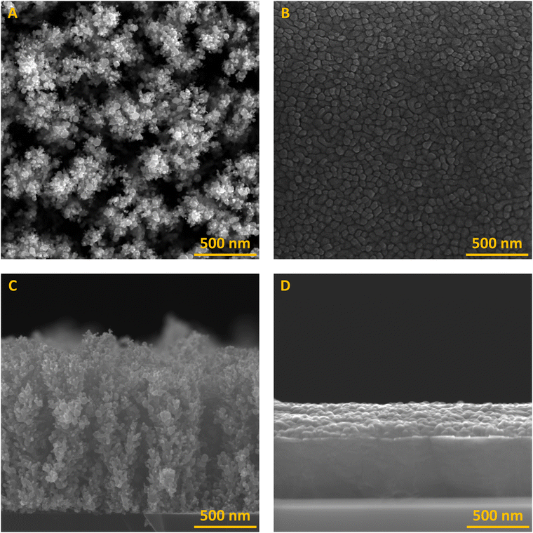 |
| | Fig. 1 Top-down views of the black gold (A) and reflective gold (B) layer taken by applying the electron microscope Tescan MIRA 3, together with the cross-section views of the black gold (C) and reflective gold (D) layers. All the pictures were taken at 100000× magnification and an accelerating voltage of 30 keV. | |
3.1.2. Energy-dispersive X-ray spectroscopy.
The energy-dispersive X-ray (EDX) spectroscopy, presented in Fig. 2, showed that the films consist of gold, carbon, and trace amounts of oxygen. The carbon contamination source originates from atmospheric carbon dioxide and hydrocarbons adsorbed on the surface (Table 1). The oxygen comes from carbon dioxide and, as later shown by the XPS, from tungsten oxide. A peak of silicon, which is very strong in the black gold spectrum, comes from the sample substrate. This indicates that the RAu layer is much more compact than the BAu layer. The absence of a difference between the chemical composition of both films proves that the difference in the film microstructures comes from a mechanism induced by gas pressure during film growth, not the presence of an impurity that influences and changes the film growth.
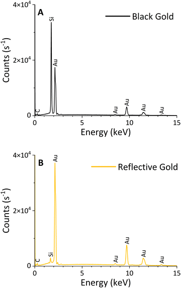 |
| | Fig. 2 EDX spectra of black (A) and reflective (B) gold acquired over 5 minutes with an accelerating voltage of 30 keV. A high silicon peak in the BAu spectrum indicates a high porosity of the layer. | |
Table 1 Chemical composition of the prepared films, according to EDX
| Film |
Gold [atom%] |
Carbon [atom%] |
Oxygen [atom%] |
| Black |
35 ± 2 |
57 ± 2 |
8 ± 1 |
| Reflective |
50 ± 2 |
44 ± 1 |
6 ± 1 |
3.1.3. X-ray photoelectron spectroscopy.
XPS measurements prove the presence of gold, tungsten, carbon, and oxygen (Table 2). The survey spectra are illustrated in Fig. 3. High resolution spectra together with their interpretation can be found in the ESI† (Fig. S1). We show that the tungsten contamination is present in the form of an oxide and most likely originates from the evaporation boat used during the deposition. Oxygen comes partially from atmospheric carbon-based contamination and partly from tungsten oxide. Carbon is present in the form of typical atmospheric contamination. For both samples, gold is found in metallic (elemental) form, proving that the nanostructuring does not lead to oxidation by atmospheric oxygen. Comparisons between several measurements over the film surface confirm the homogeneity of the sample composition.
Table 2 Chemical composition of the prepared films, according to XPS
| Film |
Gold [atom%] |
Tungsten [atom%] |
Carbon [atom%] |
Oxygen [atom%] |
| Black |
46 |
2 |
39 |
13 |
| Reflective |
53 |
2 |
31 |
14 |
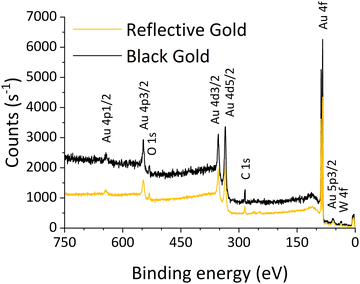 |
| | Fig. 3 XPS spectra of the samples. | |
3.1.4. Atomic force microscopy.
The surface roughness's root mean square was determined by atomic force microscopy (AFM) to be 5 nm for the RAu layer and 169 nm for the BAu layer. The images depicting the surface roughness obtained via AFM are shown in Fig. 4. The reported RMS value is half as much as the one previously reported by Hruska et al.4 for films deposited on QCM sensors. The reason is that the RMS value corresponds to the average column height on the sensor's surface. In this work, the deposited BAu layers are at 1600 nm, and the density of the film is higher, which explains the lower measured roughness. As shown in Fig. S4.1 and S4.2 (ESI†), the FFT analysis and its 2D autocorrelation proved no periodic assembly of the grains.
 |
| | Fig. 4 AFM images of the BAu (top) and RAu (bottom) layers. | |
3.1.5. X-ray diffraction analysis.
The XRD patterns for black and reflective gold possess the same number of diffraction peaks corresponding to the gold structure. The pattern was refined using a cubic structure with an Fm![[3 with combining macron]](https://www.rsc.org/images/entities/char_0033_0304.gif) m space group. The refined unit cell corresponds to a = 4.078 Å in the case of the reflective gold and a = 4.069 Å in the case of the black gold. In Fig. 5, we can notice that the reflective gold film has sharp and intense peaks contrary to the black gold width peaks, which means that the size of the gold particles in the reflective layer is larger than the size of the black gold particles. To calculate the mean crystallite size, we used the Debye equation,42 resulting in the crystallite size of reflective gold being about four times larger than that of black gold crystallites.
m space group. The refined unit cell corresponds to a = 4.078 Å in the case of the reflective gold and a = 4.069 Å in the case of the black gold. In Fig. 5, we can notice that the reflective gold film has sharp and intense peaks contrary to the black gold width peaks, which means that the size of the gold particles in the reflective layer is larger than the size of the black gold particles. To calculate the mean crystallite size, we used the Debye equation,42 resulting in the crystallite size of reflective gold being about four times larger than that of black gold crystallites.
 |
| | Fig. 5 XRD patterns of the reflective and black gold films. | |
3.2. Variable energy positron annihilation spectroscopy
Fig. 6A shows the positron lifetime spectra for RAu and BAu films measured using 1 keV positrons. Because the mean penetration depth of 1 keV positrons into gold is 2 nm, positrons are annihilated predominantly in the surface state, i.e. trapped in the image potential on the surface. One can see in Fig. 6A that the positron lifetime spectra for 1 keV positrons are very similar for RAu and BAu films, testifying that both samples have similar surface defect microstructures from the VEPAS perspective. Fig. 6B shows a comparison of the positron lifetime spectra measured using positrons with an energy of 11 keV. The mean penetration depth of 11 keV positrons into gold is 96 nm, i.e. such positrons are annihilated almost exclusively inside the gold film. Lifetime spectra measured using 11 keV positrons for RAu and BAu are substantially different. This indicates that the microstructures of RAu and BAu differ considerably. In particular, the spectrum for BAu contains a long-lived component originating from pick-off annihilations of ortho-positronium (o-Ps) formed in nanoscopic cavities.43
 |
| | Fig. 6 Positron lifetime spectra measured at positron energies of 1 keV (A) and 11 keV (B). | |
At low energies, when part of the positrons annihilates in the surface state, the mean positron lifetime is similar for both films. With increasing energy, the mean positron lifetime for the RAu film gradually decreases to a value around 0.270 ns corresponding to the annihilation of positrons trapped at vacancy clusters. In contrast, the mean positron lifetime for BAu strongly increases with rising energy owing to the higher contribution of o-Ps formed in nanoscopic pores inside the film. To obtain more detailed information, the positron lifetime spectra were decomposed into individual components. The results are presented in Fig. 7. Two components can well describe all measured spectra. The first component with a shorter lifetime corresponds to positrons annihilated as particles, i.e. not forming Ps. The lifetime of this component and its relative intensity are plotted in Fig. 7A and B, respectively. The second component represents the contribution of Ps annihilations. This component consisted of a short-lived para-positronium (p-Ps) contribution with a lifetime of 0.125 ns and a long-lived component representing the contribution of o-Ps pick-off annihilation. Because p-Ps is a singlet state and o-Ps is a triplet state, the intensity of p-Ps and o-Ps was constrained to 1:3. A lifetime of the o-Ps component is plotted in Fig. 7C, while Fig. 7D shows the total intensity of the Ps contribution. Because Ps is always formed on the surface, both films exhibit a Ps contribution with an intensity of ≈25% and an o-Ps lifetime of around 5 ns at the lowest positron energy of 0.5 keV. However, the development of the Ps contribution at higher energies when positrons penetrate the film becomes very different in RAu and BAu. In the case of the RAu film, the intensity of the Ps contribution quickly diminishes with positron energy because Ps is formed only on the surface. In contrast, in the BAu film, the intensity of the Ps contribution strongly increases with positron energy because Ps is formed not only on the surface but even more inside the film. Thus, the behaviour of the Ps contribution clearly shows that the BAu film contains nanoscopic pores, where Ps can be formed and localised. The o-Ps lifetime for the BAu also increases with energy and approaches 6.6 ns. Using the Tao–Eldrup model,44 one can calculate that the mean size of the pores in the black gold film is 1.1 ± 0.1 nm. The increasing lifetime and intensity of the o-Ps component with increasing positron energy suggest the presence of larger nanoscopic pores at greater depths and in higher concentrations. From the inspection of Fig. 7A, one can conclude that in the case of BAu film, the lifetime of the positron component increases with energy and approaches ≈0.5 ns. This is due to the contribution of positrons trapped in nanoscopic pores and annihilated there as particles. The intensity of the positron contribution (Fig. 7B) in the BAu film is lower compared to the RAu film because a significant fraction of the positrons in the BAu film form Ps. In summary, no Ps is formed inside the RAu film except for its surface. In contrast, in the BAu film, a significant fraction of the positrons form Ps. This is possible only because the BAu film contains a considerable concentration of nanoscopic pores with a mean size of ≈1.1 nm.
 |
| | Fig. 7 Results of decomposition of positron lifetime spectra for the reflective and black gold films: lifetime of positrons annihilated as particles (A); intensity of the positron annihilation contribution (B); o-Ps pick-off annihilation lifetime (C); intensity of Ps contribution (D). | |
3.3. Optical properties
3.3.1. Contact angle measurements.
The analysis of the contact angle measurements (see Table TS1, ESI†) revealed a high contrast in the wettability of the RAu and nanostructured BAu surfaces. Employing the Laplace-Young-Fitting model, the determined contact angles were estimated to be (65.3 ± 6.8)° for the RAu surface and (139.7 ± 1.7)° for the BAu surface. The interfacial tension for BAu was established at (10.7 ± 0.7) mN m−1, while the accurate determination of interfacial tension for RAu was not possible.
Notably, thoroughly cleaned bare metallic surfaces usually obtained by methods such as UV-ozone treatment are categorised as high-energy surfaces, typically exhibiting substantial wettability with extremely low or even non-measurable wetting angles.45,46 Conversely, insufficiently cleaned surfaces often manifest hydrophobic behaviour, signifying the presence of organic contaminants adsorbed on the solid surface, thereby reducing the interfacial energy of high-energy surfaces.
Furthermore, porosity or reduced layer thickness can significantly influence wetting behaviour. Additionally, highly nanostructured surfaces are more susceptible to variations in wetting owing to their increased exposure compared to solid surfaces, offering diverse possibilities for surface termination that can impact wettability. In addition, the literature extensively documents the observed hydrophobicity of highly nanostructured surfaces resulting from the entrapment of air molecules.47 These findings diverge from our earlier results acquired from thinner BAu layers prepared under identical deposition conditions, implying that the wettability of nanostructured layers highly depends on the thickness of the BM layers.2 As demonstrated, the density of BM layers diminishes in the cross-section with an increase in thickness, potentially facilitating the higher entrapment of air molecules.
3.3.2. Reflectivity and transmittance in the VIS and IR spectra.
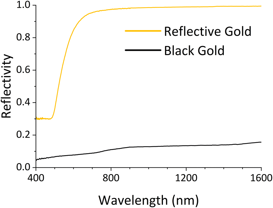
The total reflectance of the RAu and BAu samples measured in the VIS/NIR spectrum is vastly different. As shown in Fig. 8, RAu reflects nearly 100% of the incident light, in contrast to the BAu layer, which only reflects less than 20% of the incident light across the spectrum. The high absorbance of the BAu layer is caused by its surface structure. Incident light is reflected in the film, where it undergoes several reflections that are ultimately absorbed and transformed into another form of energy. Harris et al.12 observed a similar or lower diffuse reflection in the VIS region for their BAu samples. Although Harris et al.'s samples showed a slight decrease in reflection from the red to the blue end of the spectrum, our samples showed an opposite trend.
 |
| | Fig. 8 Reflectivity of the yellow and black gold layers in the VIS/NIR spectrum. | |
Room temperature IR spectra were measured in the far and middle IR ranges for both the films and the SiO2 substrate (Fig. 9A). The SiO2 glass exhibits three reflection bands below 1200 cm−1 and a broad reflectivity above 2000 cm−1. The substrate is partially transparent above 1200 cm−1. Therefore, we see the reflection of IR radiation from the back of the substrate so that the reflectance maxima correspond to the transmittance region. In contrast, the minima correspond to the absorption bands near 2200 and 3700 cm−1. IR spectra of SiO2 glasses have been reported,38 so the interpretation of their vibrational bands is not discussed. RAu has an ideal metallic behaviour, which reflects 100% of the incident's IR radiation. BAu shows a different spectrum with a minimum reflectivity near 3000 cm−1. The shape of the spectrum is typical for a conductive sample with a plasma edge near minimal reflectivity. We fit the spectrum using eqn. R(ω) = {(ε(ω)1/2 − 1)/(ε(ω)1/2 + 1)}2 and ε*(ω) = ε∞{(ωLO2 − ω2 + iωγLO)/(ωTO2 − ω2 + iωγTO)} and obtain a satisfactory fit with the parameters shown in Fig. 9B. Ilias et al.48 reported an increasing specular reflectance at 667 cm−1 with decreasing film thickness. In their report, the films with thicknesses varying from 28 to 3 μm reflected 0.2–60% of incident light. In comparison, our film with a thickness of around 1.5 μm reflected 90% of incident radiation at this wavelength, further confirming the proposed trend. Subsequently, we calculated the real parts of dielectric relative permittivity ε′ and optical conductivity σ′ spectra, as depicted in Fig. 10.
 |
| | Fig. 9 IR spectra measured in the far and middle infrared regions for the gold films and SiO2 substrate (A). 4P oscillator fit for the black gold spectrum (B). | |
 |
| | Fig. 10 Real part of the dielectric relative permittivity and optical conductivity of the black gold sample. | |
3.3.3. Electrical and gas sensing properties.
The electric resistivities of the BAu and RAu layers were 1080 and 2.1 μΩ cm, respectively. The resistivity of the BAu layer is similar to the one Takada et al. reported on black silver layers41 namely, 1 μm layers prepared at 10 and 20 Pa of argon with 1200–1400 μΩ cm resistivity. The larger resistivity of BAu is due to the low density of the film, reducing the electron path in the layer. This phenomenon is less important when the black metal film is denser, as observed for the black aluminium film deposited by magnetron sputtering. The reflective aluminium layer presented a resistivity of ∼7 μΩ cm, while the black aluminium layer presented a resistivity of ∼70 μΩ cm. In this work, the black gold layer presents a resistivity that is ∼500 times higher than the reflective gold layer. The weak density of the BAu layer is observed through the large concentration of voids measured by positron annihilation (Subsection 2.6), induced by the low coalescence process between crystallites during the film growth. This phenomenon leads to a large number of grain boundaries, which explains the difference between the resistivities of RAu and BAu. If we compare our findings with those of Becker et al.,49 we see that the resistivity of our layers is a few hundred times lower. However, it is important to note that the resistivity of the layers highly depends on their thickness.
Black gold prepared under similar conditions as the first one was also tested for its response towards oxidising agent NO2 with a concentration of 10 ppm and reducing agents CH3CH2OH, NH3 and CO with a concentration of 100 ppm at room temperature. A graphical representation of the sensor response is depicted in Fig. 11. It is apparent that the responses to distinct analytes are highly reproducible. This means that for a given analyte, all four responses in the series have a very similar shape. During the measurements, a certain drift of sensor baseline can be observed (i.e. its resistance in “pure” synthetic air) - approx. From 7.70 MΩ to 8.75 MΩ. However, such drift is predictable and does not bring serious problems to sensor applicability. Black gold exhibits typical metallic behaviour50 when exposed to oxidising gas. Its resistance starts to decrease owing to the free electrons being accepted by NO2 oxidising agent. This leads to a lower probability of mutual collisions between the free electrons, thus reducing the sensor's resistance. This electric behaviour is further affirmed by the sensor's response to the reducing agents, which increase its resistance. What is important is that similar electrical properties were reported by Becker et al. for their black gold layers.49
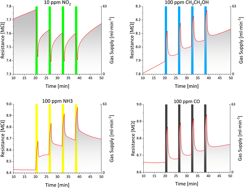 |
| | Fig. 11 Sensory response of black gold when exposed to various gas pollutants. The concentration was set to 100 ppm, except for nitrogen dioxide with a concentration of 10 ppm owing to its high toxicity. | |
In their study, they observed a positive thermal coefficient, which is typical for metallic materials. The parameters of the chemiresistors evaluated from the above-presented sensor responses (according to the methodology presented in Subsection 1.10) are summarised in Table 3. The normalized response magnitude achieves positive values for oxidizing nitrogen dioxide and negative values for the remaining (mostly reducing) analytes; hence, it corresponds to theoretical considerations. The absolute value of NRM fluctuates in the narrow range of 2.2–3.2%. For the absolute value of NRM, the response of BAu chemiresistor to the tested analytes decreases in the following order: NO2 > NH3 > CH3CH2OH > CO. An excellent parameter of BAu chemiresistors is, in general, their high SNR, ranging from 19 to 29 dB. Based on SNR, the limit of detection for a given gas can be estimated.51 In our case, with respect to high SNR values, the limit of detection is approximately two orders of magnitude lower than the tested concentrations (e.g. 100 ppb for NO2 and 1 ppm for ethanol vapours, ammonia and carbon monoxide). Finally, to comment on time constants τ obtained for the response and recovery processes, in all cases, the response time is several times shorter than its recovery counterpart (a typical feature of chemiresistors). The recorded response time values are rather uniform in the range of 19.5–25.0 seconds and also sufficiently short so that these sensors have the potential to be integrated into the early-warning systems for monitoring toxic gases.
Table 3 Sensor response parameters as measured using the SensorDataAnalyst
| NO2 |
Response |
Recovery |
| Meas. N° |
1 |
2 |
3 |
4 |
Average |
1 |
2 |
3 |
4 |
Average |
|
|
NRM [%] |
4.40 |
3.04 |
2.72 |
2.53 |
3.17 |
−2.59 |
−2.82 |
−2.73 |
−2.68 |
−2.71 |
| SNR [dB] |
25.53 |
27.20 |
28.36 |
27.70 |
27.20 |
18.13 |
23.60 |
20.82 |
24.34 |
21.72 |
|
τ [s] |
22.60 |
26.06 |
26.51 |
24.70 |
24.97 |
64.79 |
87.50 |
87.64 |
106.85 |
86.70 |
|
R
2 [%] |
99.47 |
99.20 |
99.20 |
99.49 |
99.34 |
94.36 |
95.98 |
96.04 |
96.82 |
95.80 |
| CH3CH2OH |
Response |
Recovery |
| Meas. N° |
1 |
2 |
3 |
4 |
Average |
1 |
2 |
3 |
4 |
Average |
|
|
NRM [%] |
−2.67 |
−2.69 |
−2.64 |
−2.64 |
−2.66 |
2.53 |
2.55 |
2.64 |
2.65 |
2.59 |
| SNR [dB] |
27.68 |
28.70 |
28.45 |
29.71 |
28.64 |
24.45 |
22.36 |
24.32 |
27.15 |
24.57 |
|
τ [s] |
18.39 |
18.65 |
23.33 |
17.39 |
19.44 |
91.81 |
121.45 |
127.73 |
112.76 |
113.44 |
|
R
2 [%] |
98.81 |
98.62 |
96.96 |
98.58 |
98.24 |
99.18 |
98.47 |
98.99 |
99.38 |
99.01 |
| NH3 |
Response |
Recovery |
| Meas. N° |
1 |
2 |
3 |
4 |
Average |
1 |
2 |
3 |
4 |
Average |
|
|
NRM [%] |
−2.94 |
−3.17 |
−3.18 |
−3.21 |
−3.13 |
1.33 |
2.23 |
2.55 |
3.07 |
2.62 |
| SNR [dB] |
32.33 |
35.75 |
23.03 |
21.70 |
28.20 |
15.10 |
18.80 |
19.90 |
19.63 |
19.44 |
|
τ [s] |
22.12 |
21.74 |
21.47 |
20.77 |
21.53 |
6.85 |
274.13 |
204.49 |
405.98 |
294.87 |
|
R
2 [%] |
99.29 |
99.15 |
99.02 |
99.02 |
99.12 |
82.96 |
99.60 |
99.72 |
99.74 |
99.69 |
| CO |
Response |
Recovery |
| Meas. N° |
1 |
2 |
3 |
4 |
Average |
1 |
2 |
3 |
4 |
Average |
|
|
NRM [%] |
−2.35 |
−2.39 |
−2.40 |
−2.38 |
−2.38 |
2.23 |
2.25 |
2.25 |
2.27 |
2.25 |
| SNR [dB] |
25.50 |
28.59 |
33.61 |
29.41 |
29.28 |
21.39 |
21.53 |
23.42 |
22.23 |
22.14 |
|
τ [s] |
25.23 |
22.23 |
20.10 |
18.99 |
21.64 |
77.98 |
62.48 |
54.65 |
74.59 |
67.43 |
|
R
2 [%] |
97.74 |
98.32 |
98.81 |
99.18 |
98.51 |
99.01 |
99.28 |
99.69 |
99.52 |
99.38 |
4. Conclusions
In conclusion, this study investigated various material properties of BAu layers prepared via thermal evaporation and compared them with the properties of the RAu layer prepared using the same technique. The surface morphology exhibited a high level of nanostructuring with many pores formed through the sample, resulting in a columnar structure. The chemical composition was similar for both samples, with BAu having a higher percentage of carbon-based impurities. Gold is present in the metallic form even in the BAu film, meaning that the nanostructuring does not activate its oxidation by atmospheric oxygen. As expected, surface roughness is much higher for BAu, and the crystallite size is about 4 times smaller than that of RAu. Positron annihilation spectroscopy revealed a high concentration of nanoscopic pores in the BAu layer in contrast to the RAu layer, which exhibited only crystal lattice vacancies and vacancy clusters. The contact angle measurements revealed the hydrophobic behaviour of the BAu film caused by the surface structure and gas molecule entrapment. BAu further exhibited much higher optical absorption in the VIS–NIR spectrum owing to the surface pores deflecting incident light into the film's structure, which undergoes absorption and surface plasmon resonance. The electric resistivity was about 500 times higher for the BAu film than for the RAu film. A black gold film with a similar structure also showed promising results when applied as a sensitive layer of chemiresistor. Investigation of responses to nitrogen dioxide, ethanol, ammonia and carbon monoxide proved that these responses are highly reproducible with a high signal-to-noise ratio and consequently approximated low limits of detection (as of 100 ppb NO2 and 1 ppm of remaining analytes). Moreover, the response time is sufficiently short (max. 25 s) to enable these sensors to operate in real-time monitoring systems.
Author contributions
Jan Kejzlar: conceptualization, investigation, methodology, and writing–original draft. Joris More-Chevalier: conceptualization, investigation, methodology, and validation. Martin Hruška: conceptualization, investigation, and methodology. Jaroslav Otta: conceptualization and methodology. Přemysl Fitl: supervision and funding acquisition. Michal Novotný: conceptualization, supervision, and funding acquisition. Morgane Poupon: investigation, methodology, and validation. Petr Hruška: investigation and methodology. Stanislav Cichoň: investigation and methodology. Ladislav Fekete: investigation and methodology. Veronica Goian: investigation and methodology. Stanislav Kamba: formal analysis, investigation, and validation. Jakub Čížek: investigation, methodology, and validation. Maik Butterling: methodology. Maciej Oskar Liedke: methodology. Eric Hirschmann: methodology. Andreas Wagner: methodology. Martin Vrňata: supervision and project administration. Ján Lančok: supervision and funding acquisition.
Data availability
Data for this article are available at Zenodo at https://doi.org/10.5281/zenodo.15024032.
Conflicts of interest
The authors declare that they have no known competing financial interests or personal relationships that could have appeared to influence the work reported in this paper.
Acknowledgements
The authors would like to acknowledge the support of the Ministry of Education, Youth and Sports of the Czech Republic, project No. 8F21008 and project No. JP22420 from the International Visegrad Fund. The authors also acknowledge the support of the Czech Science Foundation, Project GACR No. 23-05002S. The work is supported by Operational Programme Johannes Amos Comenius, financed by European Structural and Investment Funds and the Czech Ministry of Education, Youth and Sports (Project No. SENDISO - CZ.02.01.01/00/22_008/0004596). Parts of this research were carried out at ELBE at the Helmholtz-Zentrum Dresden-Rossendorf e. V., a member of the Helmholtz Association. We would like to thank the facility staff for assistance.
Notes and references
- P. Pokorný, M. Hruška, M. Novotný, J. More-Chevalier, P. Fitl, S. Chertopalov, T. Kiba, M. Kawamura, M. Vrňata and J. Lančok, Vacuum, 2024, 221 DOI:10.1016/j.vacuum.2023.112880.
- M. Hruška, J. Kejzlar, J. Otta, P. Fitl, M. Novotný, J. Čížek, O. Melikhova, M. Mičušík, P. Machata and M. Vrňata, Appl. Surf. Sci., 2023, 647, 158618 CrossRef.
- J. More-Chevalier, M. Novotný, P. Hruška, L. Fekete, P. Fitl, J. Bulíř, P. Pokorný, L. Volfová, Š. Havlová, M. Vondráček and J. Lančok, RSC Adv., 2020, 10, 20765–20771 RSC.
- M. Hruška, J. More-Chevalier, P. Fitl, M. Novotný, P. Hruška, D. Prokop, P. Pokorný, J. Kejzlar, V. Gadenne, L. Patrone, M. Vrňata and J. Lančok, Nanomaterials, 2022, 12(23) DOI:10.3390/nano12234297.
- M. Novotný, P. Fitl, A. Sytchkova, J. Bulíř, J. Lančok, P. Pokorný, D. Najdek and J. Boan, Open Phys., 2009, 7, 327–331 CrossRef.
- C.-M. Wang, Y.-C. Chen, M.-S. Lee and K.-J. Chen, Jpn. J. Appl. Phys., 2000, 39, 551 CrossRef CAS.
- A. Mills, Platinum Met. Rev., 2007, 51, 52 CrossRef.
- O. Melikhova, J. Cížek, P. Hruška, F. Lukác, M. Novotný, J. More-Chevalier, P. Fitl, M. O. Liedke, M. Butterling and A. Wagner, Acta Phys. Pol., A, 2020, 137, 222–226 CrossRef CAS.
- T. V. Teperik, F. J. García De Abajo, A. G. Borisov, M. Abdelsalam, P. N. Bartlett, Y. Sugawara and J. J. Baumberg, Nat. Photonics, 2008, 2, 299–301 CrossRef CAS.
- A. H. Pfund, Rev. Sci. Instrum., 1930, 1, 397–399 CrossRef CAS.
- L. Harris and A. L. Loeb, J. Opt. Soc. Am., 1953, 43, 1114 CrossRef CAS.
- L. Harris, R. T. McGinnies and B. M. Siegel, J. Opt. Soc. Am., 1948, 38, 582 CrossRef CAS.
- L. Harris, D. Jeffries and B. M. Siegel, J. Chem. Phys., 1950, 18, 261–265 CrossRef CAS.
- L. Harris, D. Jeffries and B. M. Siegel, J. Appl. Phys., 1948, 19, 791–794 CrossRef CAS.
- L. Harris and J. K. Beasley, J. Opt. Soc. Am., 1952, 42, 134 CrossRef CAS.
- L. Harris and P. Fowler, J. Opt. Soc. Am., 1961, 51, 164 CrossRef CAS.
- K. Nishio, M. Yoshida and H. Masuda, ECS Electrochem. Lett., 2013, 2, 2013–2015 Search PubMed.
- J. Kim, D. Kim, S. Y. Choi, S. D. Kim, J. Y. Song and J. Kim, Electrochim. Acta, 2016, 189, 196–204 CrossRef CAS.
- T. Zidarič, V. Jovanovski, E. Menart, M. Zorko, M. Kolar, M. Veber and S. B. Hočevar, Sens. Actuators, B, 2017, 245, 720–725 CrossRef.
- I. N. Zavestovskaya, Quantum Electron., 2010, 40, 942–954 CrossRef CAS.
- F. Fan, J. Zhang, J. Li, N. Zhang, R. R. Hong, X. Deng, P. Tang and D. Li, Sens. Actuators, B, 2017, 241, 895–903 CrossRef CAS.
- Y. Hao, S. Yang, C. Ling, D. Li, Y. Liao and Y. Zhao, ACS Appl. Nano Mater., 2022, 5, 8612–8620 CrossRef CAS.
- D. Panjwani, R. E. Peale, I. Oladeji, F. K. Rezaie, K. Baillie, J. Colwell and C. J. Fredricksen, Energy Harvest. Storage Mater. Devices, Appl. II, 2011, 8035, 80350N Search PubMed.
- J. Lehman, E. Theocharous, G. Eppeldauer and C. Pannell, Meas. Sci. Technol., 2003, 14, 916–922 CrossRef CAS.
- H. Akimoto, Science, 2003, 302, 1716–1721 CrossRef CAS PubMed.
- F. Gholami, M. Tomas, Z. Gholami and M. Vakili, Sci. Total Environ., 2020, 714, 136712 CrossRef CAS PubMed.
- C. Wang, L. Yin, L. Zhang, D. Xiang and R. Gao, Sensors, 2010, 10, 2088–2106 Search PubMed.
- S. Ma, R. Li, C. Lv, W. Xu and X. Gou, J. Hazard. Mater., 2011, 192, 730–740 CrossRef CAS PubMed.
- Q. Xiang, G. F. Meng, H. B. Zhao, Y. Zhang, H. Li, W. J. Ma and J. Q. Xu, J. Phys. Chem. C, 2010, 114, 2049–2055 CrossRef CAS.
- X. Liu, T. Ma, N. Pinna and J. Zhang, Adv. Funct. Mater., 2017, 27, 1–30 Search PubMed.
- A. B. Christiansen, G. P. Caringal, J. S. Clausen, M. Grajower, H. Taha, U. Levy, N. Asger Mortensen and A. Kristensen, Sci. Rep., 2015, 5, 1–9, DOI:10.1038/srep10563.
- V. Petříček, L. Palatinus, J. Plášil and M. Dušek, Z. Kristallogr. - Cryst. Mater., 2023, 238, 271–282 CrossRef.
- L. P. Salamakha, E. Bauer, S. I. Mudryi, A. P. Gonçalves, M. Almeida and H. Noël, J. Alloys Compd., 2009, 479, 184–188 CrossRef CAS.
- A. Wagner, M. Butterling, M. O. Liedke, K. Potzger and R. Krause-Rehberg, AIP Conf. Proc., 2018, 1970 DOI:10.1063/1.5040215.
- E. Hirschmann, M. Butterling, U. Hernandez Acosta, M. O. Liedke, A. G. Attallah, P. Petring, M. Görler, R. Krause-Rehberg and A. Wagner, J. Instrum., 2021, 16(8) DOI:10.1088/1748-0221/16/08/P08001.
- J. Čížek, Acta Phys. Pol., A, 2020, 137, 177–187 CrossRef.
-
D. B. Tanner, Optical Effects in Solids, Cambridge University Press, Cambridge, 2019 Search PubMed.
- F. Gervais, A. Blin, D. Massiot, J. P. Coutures, M. H. Chopinet and F. Naudin, J. Non-Cryst. Solids, 1987, 89, 384–401 Search PubMed.
-
M. Hruška, University of Chemistry and Technology, 2024 Search PubMed.
- P. Hruška, J. More-Chevalier, M. Novotný, J. Čížek, O. Melikhova, L. Fekete, M. Poupon, J. Bulíř, L. Volfová, M. Butterling, M. O. Liedke, A. Wagner and P. Fitl, J. Alloys Compd., 2021, 872 DOI:10.1016/j.jallcom.2021.159744.
- K. Takada, M. Kawamura, T. Kiba, Y. Abe, M. Ueda and M. Hruška, Appl. Phys. A: Mater. Sci. Process., 2024, 130 DOI:10.1007/s00339-024-07328-7.
- P. Debye, Ann. Phys., 1915, 351, 809–823 CrossRef.
- S. J. Tao, J. Chem. Phys., 1972, 56, 5499–5510 CrossRef CAS.
- K. Wada and T. Hyodo, J. Phys.: Conf. Ser., 2013, 443(1) DOI:10.1088/1742-6596/443/1/012003.
- E. Bormashenko, A. Musin and M. Zinigrad, Colloids Surf., A, 2011, 385, 235–240 CrossRef CAS.
-
E. Y. Bormashenko, Wetting of Real Surfaces, De Gruyter, Berlin, 2013 Search PubMed.
-
L. Duta, A. C. Popescu, I. Zgura, N. Preda and I. N. Mihailescu, in Wetting and Wettability, InTech, 2015, p. 384 Search PubMed.
- S. Ilias, P. Topart, C. Larouche, P. Beaupré, D. Gay, C. Proulx, T. Pope and C. Alain, Photonics North, 2010, 7750, 77501J Search PubMed.
- W. Becker, R. Fettig and W. Ruppel, Infrared Phys. Technol., 1999, 40, 431–445 CrossRef CAS.
-
J. S. Dughale, The Electrical Properties of Metals and Alloys, Courier Dover Publications, 2016 Search PubMed.
- T. He, W. Liu, T. Lv, M. Ma, Z. Liu, A. Vasiliev and X. Li, Sens. Actuators, B, 2021, 329, 129275 CrossRef CAS.
|
| This journal is © The Royal Society of Chemistry 2025 |
Click here to see how this site uses Cookies. View our privacy policy here. 
 Open Access Article
 This Open Access Article is licensed under a
  *ab,
Joris
More-Chevalier
*ab,
Joris
More-Chevalier