
 Open Access Article
 This Open Access Article is licensed under a
 Creative Commons Attribution 3.0 Unported Licence
Impedance spectroscopy and optical properties of lanthanum-modified Bi2FeMnO6 for NTC thermistor applications
Laxmidhar
Sahoo
a,
Swayam Aryam
Behera
 a,
P.
Ganga Raju Achary
a and
S. K.
Parida
*b
a,
P.
Ganga Raju Achary
a and
S. K.
Parida
*b
aDepartment of Chemistry, ITER, Siksha O Anusandhan Deemed to be University, Bhubaneswar-751030, India
bDepartment of Physics, ITER, Siksha O Anusandhan Deemed to be University, Bhubaneswar-751030, India. E-mail: santoshparida@soa.ac.in
First published on 22nd January 2025
Abstract
The double perovskite Bi1.75La0.25FeMnO6 (BLFMO) ceramic was prepared by a solid-state reaction method and characterized by different techniques such as X-ray diffraction, scanning electron microscope, energy dispersive X-ray, transmission electron microscope, and optical, dielectric, and electrical property analysis. The synthesized material has a monoclinic crystal structure with an average crystallite size of 63.7 nm and lattice strain of 0.0013, as revealed by X-ray diffraction (XRD) data. The surface morphology of the prepared sample was studied by the scanning electron microscope (SEM) technique, which shows spherical-shaped well-developed grains having clear grain boundaries with an average grain size of 55.6 μm. The EDX spectrum and elemental color mapping checked the purity and homogeneity of the sample. The transmission electron microscope (TEM) technique displayed that the particles are well connected in the synthesized material, which may be a possible reason for the better physical properties. The Brunauer–Emmet–Teller (BET) surface area was 0.371 m2 g−1, with a pore volume of 7.202 cc g−1 and an average pore diameter of 19.635 Å. The optical properties were studied from Fourier transform infrared (FTIR) and ultraviolet diffuse reflectance spectroscopy (UV-DRS). The FTIR spectrum revealed the vibrational modes of all the constituent elements in the sample. The direct bandgap energy of 2.71 eV was calculated from the UV-DRS spectrum, which is suitable for optoelectronic device applications. The sample exhibited high dielectric constant, low loss (from dielectric study), negative temperature coefficient of resistance behavior (from impedance study), non-Debye relaxation (from modulus study), and a thermally activated conduction mechanism (from ac conductivity study). The occurrence of Maxwell–Wagner dispersion was known from the dielectric study. The semi-circular arcs in the Nyquist and Cole–Cole's plots explained their semi-conducting nature. The resistance versus temperature curve indicated the semiconducting nature of the sample and its potential application as a negative temperature coefficient (NTC) thermistor. Thus, the prepared sample has unique characteristics for different applications related to optoelectronics and sensors.
1. Introduction
In modern times, double perovskite compounds have drawn much attention from research communities and material scientists because of their cost-effective preparation, remarkably bipolar charge mobility, variable bandgap energy, broad range absorption coefficient, highly scalable production technique, and tunability of functional characteristics. Double perovskites may be better than single perovskites due to increased oxygen vacancies, more capacity to acquire additional atoms, and complex structure. Hence they have enriched physical properties, better chemical stability, and potential applications.1 Moreover, the improved dielectric properties and transport mechanism in the double perovskites may be suitable for multilayer capacitors, memory chips, and microelectronic devices.2–4 The general formula for a double perovskite can be written as AA′B2O6 or A2BB′O6 by occupying the two different cations in the A- or B-sites (A = rare-earths and alkaline earth metal, B = transition metals).5–8 The magnetic properties of double perovskites are governed by the exchange and super-exchange mechanisms of B and B′, respectively, through an oxygen atom and act as a ferrimagnetic insulator due to half metallicity and high Curie temperature. Furthermore, for double perovskite oxides A2B′B′′O6 with Bi at the A-site, the ferroelectric order is due to the large orbital radius of the 6s2 lone pair electrons of the Bi and the magnetic order is due to partially filled 3d orbitals of B-site transition metal ions.9,10 Again, lead-free double perovskites are better than lead-based perovskites (which are toxic) because of their property-application relation and eco-friendly nature. Bismuth-based double perovskites are a better alternative to lead-based perovskites, among all other kinds of double perovskites. However, the synthesis of single-phase bismuth-based perovskites is a challenging task regarding stabilization due to the high volatility of bismuth and affinity for multiphase formation.11 It is reported that the stability of single-phase Bi-based perovskites can be improved by partial replacement of Bi ions with a small amount of La ions.11 The La3+ cation can partially replace the Bi3+ cation to support stabilization. It has been demonstrated that partial substitution of La3+ cations for Bi3+ cations on the A-site can allow single-phase stabilization in bismuth manganite compounds. This is because La3+ has an ionic radius (0.130 nm) which is somewhat smaller than that of Bi3+ (0.131 nm).12In this connection, we have studied double perovskite compounds such as Bi2FeMoO6,13 La2MnNiO6,14 and Bi2MnMoO615 which were used in the magnetic tunnel junction (MTJ) electrodes for spintronics. Osaka et al.16 have reported the compound, Ca2FeMnO6 as a layered double perovskite with a charge-disproportioned crystal structure and its crystal structure is P21/c.
Zhao et al.17,18 synthesized Bi2FeMnO6 ceramics by a conventional solid-state reaction method using Bi2O3, Fe3O4, and MnCO3 as starting materials with 10 mol% extra Bi2O3. The impure phase of Bi2Fe4O9 was detected in the Bi2FeMnO6 ceramic and to stabilize the metastable phase of it, the partial replacement of Bi by La (20 mol%) in Bi2FeMnO6 was performed. They found that the La-doped Bi2FeMnO6 ceramics exhibited a spin glass state at low temperatures with a Néel temperature (TN) below room temperature.17 Delmonte et al.19 prepared the metastable Bi2FeMnO6 ceramics via a solid-state reaction under high pressure (6 GPa) and temperature (1100 °C for 1.5 h). Some eco-friendly lead-free halide double perovskites comprising the general chemical formula Cs2AgBiX6 (X = Cl or Br) have also been found to be very attractive for optoelectronic behaviors.20 Recently, some Bi-based perovskites/double perovskites, like Bi(Zn0.5Ti0.5)O3,21 BiCaFeCeO6,22 BiZn2VO6,23 BiHoZnZrO6 and BiHoCuTiO624 have been found to be very promising for multifunctional applications because of their excellent ferroelectric and ferromagnetic properties. Some cerium-modified bismuth-layered ferroelectrics, namely SrBi2Ta2O9,25,26 cerium-substituted HAp (hydroxyl apatite) ceramic,27 and Ca, Ce-doped BaTiO3 ceramic28 have also been reported for this purpose.
A lead-free halide double perovskite: Cs2AgBiBr6 has an energy bandgap of 1.95 eV, which may be suitable for photovoltaic and solar cell applications.29–32 The ability to change the energy bandgap in the double perovskite materials using different dopants has vast demand for solar cell applications. Islam et al. investigated recently a set of La2−xSrxCoMnO6 double perovskites and reported the energy bandgap of 1.37 eV as a better candidate for solar cell application.33 Again, double perovskites La2B′MnO6 (B′ = Ni, Co, or other transition elements) have been investigated to explore the multifunctional applications in the field of science and technology.34–37
After studying the above literature reports, we have synthesized a new Bi1.75La0.25FeMnO6 double perovskite using the solid-state reaction method and explored the possibility of new properties through some of the characterizations by various techniques. XRD analysis has been carried out to find the crystal structure and crystallite size of 63.7 nm. The SEM technique has been used to calculate the average grain size and understand the grain boundary effect. The EDX spectrum and elemental mapping have been used to confirm the purity and homogeneity of the sample. The optical properties are studied from FTIR and UV-DRS techniques. The impedance spectroscopy study has been carried out to determine the dielectric, impedance, modulus, and conductivity properties of the synthesized sample over a wide range of frequencies (1 kHz to 1 MHz) and temperatures (25 °C to 500 °C).
This comprehensive investigation enabled us to determine the optical, dielectric, impedance, modulus, and conductivity properties of the Bi1.75La0.25FeMnO6 ceramic. The experimental data provide a thorough understanding of the material's electrical behavior and its potential applications in electronic devices. The material is abbreviated in the whole manuscript as BLFMO for convenience and to avoid undesired repetition.
2. Experiment and techniques
2.1 Raw materials used
Bi2O3, La2O3, FeCO3, and MnO2 are the raw materials used for getting the final product of Bi1.75La0.25FeMnO6 ceramic. The essential raw ingredients are obtained with greater than 99% purity from Loba Chemical Pvt. Ltd. In the digital balance of least count 0.0001, the raw components are weighed. For the newly prepared sample, the final chemical equation is:| 0.875Bi2O3 + 0.125La2O3 + FeCO3 + MnO2 → Bi1.75La0.25FeMnO6 + CO2↑ |
2.2 Synthesis method
Using an agate mortar and pestle, the measured raw materials were mixed for two hours in the dry medium and for another two hours in the wet medium using 10 ml methanol. The final product was formed by calcinating the powdered sample at 850 °C. After that, a pinch of powdered sample was sent for XRD analysis for phase confirmation. A uniaxial pressure of 4 × 10⁶ Pa was used to make two cylindrical pellets with a diameter of 12 mm and a thickness of 2 mm, using polyvinyl alcohol (PVA) as the binder. The calcinated powders were maintained 50 °C above the calcination temperature to eliminate the impurity signal and achieve high densification. The pellets were then sintered at 900 °C, making them suitable for further characterization and investigations.2.3 Characterization techniques
The structural analysis of the prepared sample was done using the X-ray diffraction data [MODEL: RIGAKU Japan ULTIMA IV; equipped with a source of CuKα radiation (λ = 1.5405 Å)]. The XRD data were recorded at the scanning rate of 3° per minute from a wide range of Bragg's angles, 20° to 80°. An energy dispersive X-ray analysis (SEM-EDX; MODEL: ZEISS; EVO-18) equipped with a scanning electron microscope using an accelerating voltage of 2000 kV and a working distance of 9270 μm was used to analyze the composition of the prepared sample, and produce microstructural micrographs and surface morphology. Using a 2000 kV working potential, transmission electron microscopy (TEM) (Model: JEOL JEM-F 200) was used to analyze the size distribution and connectivity form of particles of the material under study. Both sides of a pellet have two layers of silver coating to improve electrode performance for electrical measurements. To comprehend atomic vibrations, FTIR data were studied using the Jasco FTIR-4600LE machine. The dielectric and electrical characteristics were measured at frequencies between 1 kHz to 1 MHz and temperatures between 25 °C to 500 °C using the impedance analyzer (Model No. N4L PSM, 1735). The prepared material's direct bandgap energy was determined using UV-visible spectroscopy with MODEL: V670 and Sl. No. A050461154. The following section describes the structural, microstructural, surface area measurement, optical, dielectric, and electrical characterizations to go into further depth about the results of the prepared sample.3. Results and discussion
3.1 Sample formation
The tolerance factor of the prepared ceramic material can be calculated using the relation:where rA = ionic radius of atom A, rB = ionic radius of atom B, and r0 = ionic radius of an oxygen atom to check the formation of a stable perovskite material.38 However, the modified relation for a double perovskite can be written as;
where RA′, RA′′, RB′, RB′′, and RO are known to be the ionic radii of Bi, La, Fe, Mn and O, respectively.39,40 The tolerance factor of the synthesized material was calculated as 0.88, which supports a stable double perovskite formation in a monoclinic crystal structure.
3.2 XRD analysis
The XRD method contributes to recognizing unidentified structures, unit cells, space groups, density, and volume of a material. Fig. 1(a) indicates the XRD pattern of the calcinated and powdered BLFMO ceramic material. | ||
| Fig. 1 (a) XRD pattern analysis and (b) Williamson–Hall plot of the Bi1.75La0.25FeMnO6 ceramic. | ||
A single-phase monoclinic crystal structure appears to have formed, according to the preliminary structural study. The POWDMULT software is employed to determine the crystal structure and lattice parameters41 of this material. The monoclinic crystal structure is predicted by structural analysis when the computed and experimental (observed) inter-planner distances agree as much as possible with the least amount of standard deviation. Using the monoclinic crystal structure, POWDMULTs software indexes all the prominent XRD peaks. The evaluated cell parameters of the synthesized material are a = 6.5602 Å, b = 3.9257 Å, c = 3.9712 Å having β = 101.65° and V = 100.16 Å3. The crystalline nature of the prepared sample is shown by the peak's clarity and sharpness. The monoclinic crystal symmetry of this material is used for investigating structural properties. Fig. 1(b) indicates the Williamson–Hall plot of the prepared material. By using the Williamson–Hall formula;

3.3 Microstructural analysis (SEM study)
Fig. 2(a) shows the surface microstructure (SEM micrograph), (b) Gaussian fitted grain size, (c) EDX spectrum, and (d) elemental color mapping of the BLFMO ceramic. The SEM micrograph reveals nano-cubical-shaped grains that are uniformly dispersed across the surface of the BLFMO ceramic. Well-defined grain boundaries are observed and the compactness of the grains indicates the absence of significant voids in this material. The microstructure contributes to better electrical conductivity, which will be further explained in the AC conductivity section. | ||
| Fig. 2 (a) SEM micrograph, (b) Gaussian fitted grain size, (c) EDX spectrum, and (d) elemental color mapping of the Bi1.75La0.25FeMnO6 ceramic. | ||
The Gaussian fitted grain size analysis indicates that the distribution of grain sizes follows a normal (Gaussian) distribution. The average grain size is found to be 55.60 μm with a standard deviation of 1.61, which is calculated by taking 60 grains from the SEM micrograph using ImageJ software. This information provides an insight into the homogeneity of the ceramic material. The EDX spectrum analysis confirms the presence of all constituent elements (Bi, La, Fe, Mn, and O) in the BLFMO ceramic. The elemental composition is found to be consistent both in terms of weight and atomic percentage. This analysis provides crucial information about the chemical composition of the synthesized material. The elemental color mapping of the prepared sample indicates the homogeneous distribution of constituent elements and it is known that all the constituent elements are present, and their distribution over the sample surface is uniform. This visual representation helps in understanding the spatial distributions in elemental composition. The combination of SEM micrograph analysis, Gaussian fitted grain size, EDX spectrum, and elemental color mapping provides a comprehensive understanding of the microstructure, elemental composition, and distribution of the BLFMO ceramic at the nanoscale. The observed features such as well-defined grain boundaries and uniform distribution of elements contribute to the improved electrical conductivity mechanism of the material, which helps the researchers working on materials with specific electronic or functional properties.
3.4 TEM study
Transmission electron microscopy (TEM) provides an extremely high spatial resolution, allowing researchers to examine the microstructure of ceramics at the atomic or nanoscale. TEM can provide detailed crystallographic information that is to identify crystal structures, grain boundaries, and defects within the ceramic materials. This information is essential for understanding the mechanical, electrical, and thermal properties of ceramics. Fig. 3 shows the TEM micrograph of the BLFMO ceramic. All particles of the synthesized sample display a nearly spherical morphology; however, the particle sizes are not uniform because of some degree of agglomeration, due to the high surface energy of the nanoparticles, the agglomerate phenomenon of BLFMO particles can be seen in Fig. 3.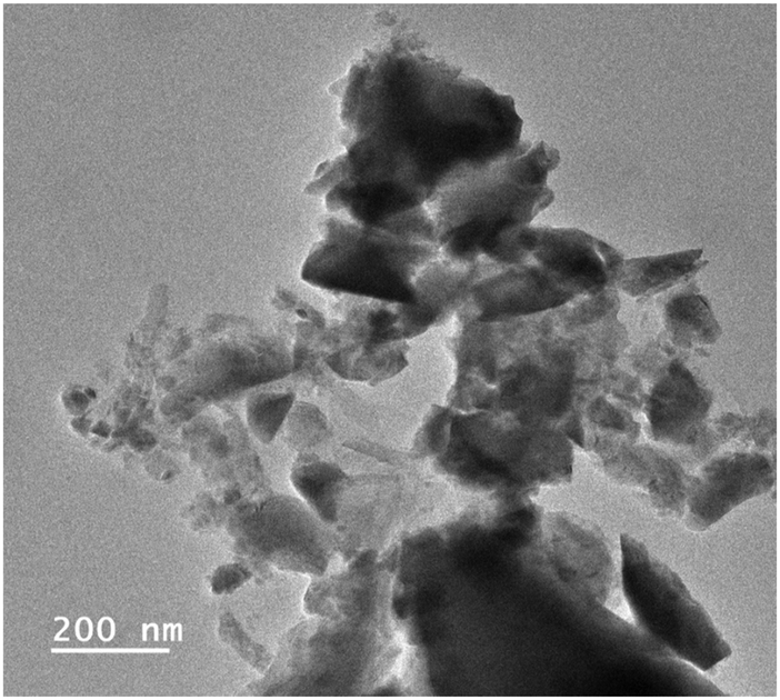 | ||
| Fig. 3 TEM image of the Bi1.75La0.25FeMnO6 ceramic. | ||
3.5 BET surface area measurement
The BET (Brunauer–Emmett–Teller) analysis was conducted to analyze the N2-sorption isotherms of the prepared material, Bi1.75La0.25FeMnO6, which is shown in Fig. 4. The surface area was found to be 0.371 m2 g−1, with a pore volume of 7.202 cc g−1 and an average pore diameter of 19.635 Å. The isotherm exhibits type IV adsorption behavior, indicating that the material is mesoporous with a small hysteresis loop.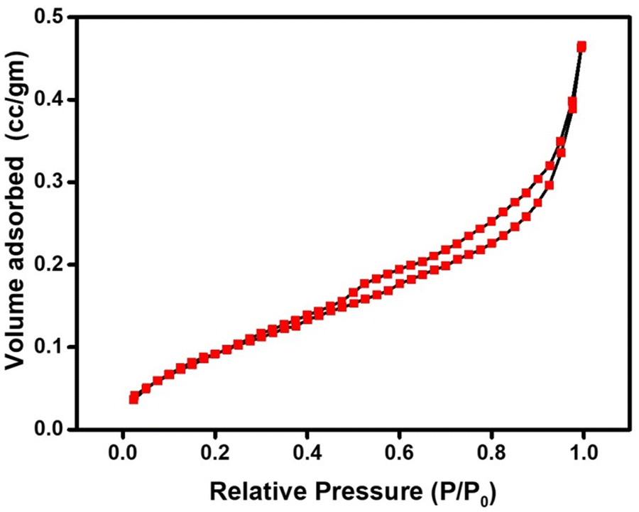 | ||
| Fig. 4 Nitrogen sorption isotherms of the compound Bi1.75La0.25FeMnO6. | ||
3.6 Optical properties
The optical properties of this material have been studied with the help of FTIR and UV-DRS analysis.Fig. 5(a) represents the FTIR spectrum of the BLFMO ceramic at room temperature and bands are observed at 3837 cm−1, 3747 cm−1, 3564 cm−1, 2922 cm−1, 2359 cm−1, 1557 cm−1, 1455 cm−1 and 1115 cm−1, respectively.
 | ||
| Fig. 5 (a) FTIR, (b) absorbance spectrum, and (c) energy versus (αhν)2 for direct allowed transitions to calculate the bandgap energy of the Bi1.75La0.25FeMnO6 ceramic. | ||
Fourier transform infrared (FTIR) analysis is a valuable technique for studying the molecular composition of a material. In the context of the BLFMO ceramic, the provided FTIR spectrum (Fig. 5(a)) indicates several absorption bands at specific wavenumbers. The bands at 3837 cm−1 and 3747 cm−1 are likely associated with stretching vibrations of hydroxyl (OH) groups or water molecules.44,45 The presence of these bands could be indicative of surface-adsorbed water or hydroxyl groups on the ceramic. The band at 2359 cm−1 is in a region where carbon dioxide (CO2) typically absorbs. It might indicate the presence of carbon dioxide, possibly from the surrounding environment. The band at 1557 cm−1 could be related to the stretching vibrations of C![[double bond, length as m-dash]](https://www.rsc.org/images/entities/char_e001.gif) O bonds, suggesting the presence of carbonyl groups. The exact nature of these carbonyl groups would depend on the specific molecular composition of the ceramic. The band at 1455 cm−1 might be associated with bending vibrations of CH2 groups or other organic moieties. The presence of organic compounds or groups can be inferred from this absorption. The broad bands at 570 to 1115 cm−1 may be related to the stretching vibrations of Bi–O stretching vibration, Mn–O stretching vibration, La–O stretching vibration and Fe–O stretching vibrations confirming the octahedral FeO6 present in the synthesized sample.46–49 The exact interpretation would depend on the specific chemical environment. In summary, FTIR analysis of the BLFMO ceramic reveals absorption bands at various wavenumbers, each providing information about specific molecular vibrations and functional groups present in the material. The interpretation of these bands allows researchers to gain insights into the chemical composition and bonding characteristics of the ceramic, thereby strengthening the phase confirmation and expanding the understanding of its properties.
O bonds, suggesting the presence of carbonyl groups. The exact nature of these carbonyl groups would depend on the specific molecular composition of the ceramic. The band at 1455 cm−1 might be associated with bending vibrations of CH2 groups or other organic moieties. The presence of organic compounds or groups can be inferred from this absorption. The broad bands at 570 to 1115 cm−1 may be related to the stretching vibrations of Bi–O stretching vibration, Mn–O stretching vibration, La–O stretching vibration and Fe–O stretching vibrations confirming the octahedral FeO6 present in the synthesized sample.46–49 The exact interpretation would depend on the specific chemical environment. In summary, FTIR analysis of the BLFMO ceramic reveals absorption bands at various wavenumbers, each providing information about specific molecular vibrations and functional groups present in the material. The interpretation of these bands allows researchers to gain insights into the chemical composition and bonding characteristics of the ceramic, thereby strengthening the phase confirmation and expanding the understanding of its properties.
The use of UV visible spectroscopy supports the explanation of the sample's semiconducting nature. Tauc's relation can be used to calculate the band gap energy of the sample, which will reveal the potential optoelectronic application of the sample.50,51 The UV-visible absorbance spectra recorded for the prepared ceramic are shown in Fig. 5(b) over a broad range of wavelengths, 300–800 nm. The optical bandgap energy (Eg) is determined using the experimental data and using Tauc's relation, (αhv)1/n = A(hν − Eg), where hν is energy (in units of eV), A is a constant (independent of photon energy), and Eg is the optical bandgap energy.52,53 The electronic transition index (n) has values of 1/2 and 3/2 for direct permitted and forbidden transition types, and 2 and 3 for indirect permitted and forbidden transition types. The direct allowed transition of the prepared sample is shown in Fig. 5(c), based on the plotted spectrum. The energy versus (αhv)2 plot in this study gives a directly allowed bandgap energy (Eg) of 2.71 eV through a straight-line extrapolation.54 This bandgap energy value falls within an appropriate range for use in photovoltaic and photocatalytic processes.
3.7 Dielectric study
The ability of a material to store electrical charges and consequently, energy from an applied electric field can be ascertained using relative dielectric permittivity (εr). The field strength in a material medium is divided by the field strength in a vacuum medium and is used to calculate εr. The atoms and molecules of a material vibrate when it is exposed to an electric field because of the material's charge development. Consequently, the forced displacement of the charged ions from their equilibrium site increases polarization. The value of the real and imaginary part of the dielectric constant and dielectric loss can be calculated from the recorded dielectric data using the relation:
and

where εs and ε∞ denote the static dielectric constant and dielectric constant at very high frequency, respectively, ω is the angular frequency and τ is the relaxation time. The dielectric properties of the perovskite material can be studied from the variation of dielectric constant and dielectric loss with both frequency and temperature. The dielectric constant can be found using the formula; εr = Cp/C0, where C0 = ε0A/t, ε0 = 8.85 × 10⁻¹² F m−1, t = thickness of the pellet and A = area of the cross-section of the pellet. It is well known that dielectric properties depend upon the polarization process in the material after the application of an external AC electric field.55–57

The change in dielectric constant with frequency at different temperatures, from 25 °C to 500 °C is shown in Fig. 6(a). At low frequencies, a highly dielectric dispersion is seen, which gradually decreases as the frequency increases. Maxwell–Wagner polarization theory58 provides strong support for the observation of a broad dielectric dispersion at low frequencies, which is due to the accumulation of electrons near the grain boundaries, causing high resistance space charge polarization at the interface of the grain boundaries. According to Maxwell–Wagner theory, the sample exhibits four different types of polarization at low frequencies: electronic, dipolar, ionic, and space charge polarization. However, the space/interfacial polarizations contribute the most. Once more, the dielectric constant decreases with increasing frequency due to a decrease in space charge polarization.59 Additionally, as seen in Fig. 6(a), a steep slope is observed that appears to be quite steep at a low-frequency region (which may correspond to the grain boundary effect) and shallow at a high-frequency region (which may correspond to the grain effect). Moreover, Koop's two-layer model theory60 can explain the high dielectric dispersion nature of this material.
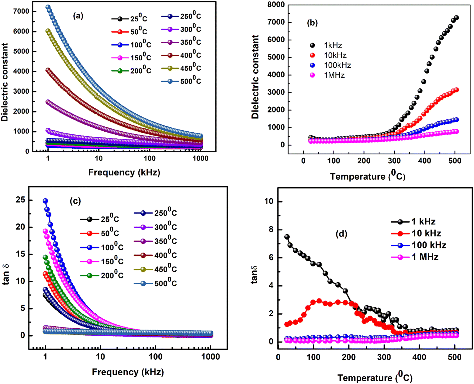 | ||
Fig. 6 (a) Dielectric constant versus frequency, (b) dielectric constant versus temperature of the Bi1.75La0.25FeMnO6 ceramic. (c) tan![[thin space (1/6-em)]](https://www.rsc.org/images/entities/char_2009.gif) δ versus frequency and (d) tanδ versus temperature of the Bi1.75La0.25FeMnO6 ceramic. δ versus frequency and (d) tanδ versus temperature of the Bi1.75La0.25FeMnO6 ceramic. | ||
Fig. 6(b) represents the change of dielectric constant against temperature at selected frequencies ranging from 1 kHz to 1 MHz. From this figure, it is observed that the dielectric constant has a low value at low temperatures which is due to the inert nature of the ions and polarons, and passiveness of mobile electrons, and also charge carriers are less thermally activated as well as less mobile.61 Then, the dielectric constant increases with the increase in temperature, which is due to the involvement of thermally active mobile charge carriers’ activation of electron hopping and electronic dispersal between Fe2+ and Fe3+ ions and the presence of space charge polarization.
Fig. 6(c) represents the change of dielectric loss (tanδ) against frequency at selected temperatures ranging from 25 °C to 500 °C. From this figure, it is observed that there is a wide dispersion of dielectric loss at low-frequency regions and it is due to the misalignment of electric dipoles. This is explained by Maxwell–Wagner theory and according to this theory, a dielectric medium supports strongly that conducting grains are sensitive near high frequency and resistive grain boundaries are sensitive near low frequency. At low frequency, mobile ions between Fe2+ and Fe3+ hop at their respective octahedral locations, but this hopping process is suppressed at high frequency and this is due to quick change of the supplied external AC field. Dielectric loss (tanδ) has a low value at the high-frequency zone, which is due to the reduction of space charge polarization and decreasing thermal agitation and misalignment.59
Fig. 6(d) represents the change of dielectric loss (tanδ) against temperature at selected frequencies ranging from 1 kHz to 1 MHz. A rise in tanδ with temperature is observed in Fig. 6(d), which is due to the increased vibrational movement of ferrite ions at the octahedral site and the existence of defects/impurities or oxygen vacancies, which ultimately results in increased space charge polarization.61 Consequently, tanδ predicts energy dissipation and detects impurities and defects under the influence of a field. Thus, the sample has a low dielectric loss and high dielectric constant, hence making it a suitable candidate for an energy storage device.
3.8 Impedance study
The relationship between the electrical and microstructural properties of a material is revealed through impedance analysis. This technique explains the electrical properties of the material including the quality of the material or ceramic formation, bulk (grain), grain boundaries, transport qualities, and charge storage capacity. The frequency against real and imaginary impedance (Z′ and Z′′) at various chosen temperatures (25 °C to 500 °C) is shown in Fig. 7(a) and (b). The interpretation of these impedance components provides a valuable understanding of the electrical behavior and properties of the material under investigation. It is observed from Fig. 7(a) that the value of Z′ decreases at the low-frequency region when the temperature increases. This behavior is characteristic of the negative temperature coefficient resistance (NTCR) nature.62 It is a well-known fact that the resistance decreases with an increase in temperature in NTCR materials, which is usually observed in certain semiconductors.63 This behavior is significant for applications where temperature sensing or temperature compensation is required. At high frequencies (above 10 kHz), the Z′ values completely merge irrespective of temperatures supporting the semiconducting nature, and also the release of interfacial charges contributes to this behavior.64,65 The imaginary component of impedance (Z′′) adopts the same fashion as Z′, as described in Fig. 7(b). The behavior of Z′′ also supports the NTCR behavior at low frequencies and the semiconducting properties at high frequencies, as discussed for Z′. The graph between Z′ and Z′′ at selected temperatures (25 °C to 500 °C), called Nyquist plots, is shown in Fig. 7(c). The presence of the semi-circular arcs in the Nyquist plots confirms the semiconductor character of the synthesized sample.66Fig. 7(d) shows the fitted Nyquist plots at some selected temperatures. The Nyquist data were fitted with an equivalent (CQR)(CR) circuit using the ZSIMPWIN version 2.0 software. The calibrated fitting parameters are bulk resistance (Rb), bulk capacitance (Cb), constant phase factor (Q), grain boundary capacitance (Cgb), grain boundary resistance (Rgb), and frequency power (n) which are reported in Table 1. The decrease of both bulk resistance from 6.019 × 10⁴ Ω at 25 °C to 1.118 × 10³ Ω at 100 °C and grain boundary resistance from 3.034 × 10⁴ Ω at 25 °C to 9.168 × 10³ Ω at 500 °C supports the semiconducting and NTCR nature of the synthesized sample. | ||
| Fig. 7 (a) Z′ versus frequency, (b) Z′′ versus frequency, (c) Nyquist plot, and (d) fitted Nyquist plots of the Bi1.75La0.25FeMnO6 ceramic. | ||
| Temp. (°C) | C b (F cm−2) | Q (s−5 cm−2) | R b (Ω cm2) | n | C gb (F cm−2) | R gb (Ω cm2) |
|---|---|---|---|---|---|---|
| 25 | 1.165 × 10⁻¹⁰ (Expt.) | 1.979 × 10⁻⁸ (Expt.) | 6.019 × 10⁴ (Expt.) | 1.56 | 3.134 × 10⁻¹⁰ (Expt.) | 3.034 × 10⁴ (Expt.) |
| 1.165 × 10⁻¹⁰ (fitting) | 1.979 × 10⁻⁹ (fitting) | 6.019 × 10⁴ (fitting) | 3.134 × 10⁻¹⁰ (fitting) | 3.034 × 10⁴ (fitting) | ||
| 50 | 1.000 × 10⁻²⁰ (Expt.) | 7.039 × 10⁻⁹ (Expt.) | 4.333 × 10⁴ (Expt.) | 13.8 | 2.462 × 10⁻¹⁰ (Expt.) | 3.588 × 10⁴ (Expt.) |
| 1.607 × 10⁻²¹ (fitting) | 7.030 × 10⁻¹⁰ (fitting) | 4.335 × 10⁴ (fitting) | 2.463 × 10⁻¹⁰ (fitting) | 3.587 × 10⁴ (fitting) | ||
| 100 | 6.739 × 10⁻¹⁶ (Expt.) | 1.320 × 10⁻⁷ (Expt.) | 1.118 × 10³ (Expt.) | 51.6 | 1.452 × 10⁻¹⁰ (Expt.) | 3.793 × 10⁴ (Expt.) |
| 5.208 × 10⁻¹⁶ (fitting) | 1.366 × 10⁻⁸ (fitting) | 1.061 × 10³ (fitting) | 1.449 × 10⁻¹⁰ (fitting) | 3.798 × 10⁴ (fitting) | ||
| 150 | 1.000 × 10⁻¹⁵ (Expt.) | 2.143 × 10⁻¹⁰ (Expt.) | 3.333 × 10⁴ (Expt.) | 9.84 | 1.159 × 10⁻⁸ (Expt.) | 3.093 × 10³ (Expt.) |
| 1.000 × 10⁻¹⁵ (fitting) | 2.143 × 10⁻¹⁰ (fitting) | 3.333 × 10⁴ (fitting) | 1.159 × 10⁻⁸ (fitting) | 3.093 × 10³ (fitting) | ||
| 200 | 1.000 × 10⁻²⁰ (Expt.) | 1.407 × 10⁻⁶ (Expt.) | 2.385 × 10⁴ (Expt.) | 10.1 | 2.475 × 10⁻¹⁰ (Expt.) | 2.098 × 10⁴ (Expt.) |
| 2.829 × 10⁻²⁹ (fitting) | 1.407 × 10⁻⁹ (fitting) | 2.385 × 10⁴ (fitting) | 2.475 × 10⁻¹⁰ (fitting) | 2.098 × 10⁴ (fitting) | ||
| 250 | 1.706 × 10⁻¹⁰ (Expt.) | 3.863 × 10⁻⁷ (Expt.) | 3.953 × 10⁴ (Expt.) | 5.30 | 1.236 × 10⁻⁹ (Expt.) | 2.219 × 10⁴ (Expt.) |
| 1.706 × 10⁻¹⁰ (fitting) | 3.867 × 10⁻⁹ (fitting) | 3.953 × 10⁴ (fitting) | 1.236 × 10⁻⁹ (fitting) | 2.218 × 10⁴ (fitting) | ||
| 300 | 1.903 × 10⁻¹⁰ (Expt.) | 1.452 × 10⁻⁸ (Expt.) | 4.793 × 10⁵ (Expt.) | 2.40 | 2.445 × 10⁻⁹ (Expt.) | 9.868 × 101 (Expt.) |
| 1.903 × 10⁻¹⁰ (fitting) | 1.451 × 10⁻⁸ (fitting) | 4.793 × 10⁵ (fitting) | 2.447 × 10⁻⁹ (fitting) | 9.857 × 101 (fitting) | ||
| 350 | 1.544 × 10⁻¹⁰ (Expt.) | 3.116 × 10⁻⁸ (Expt.) | 1.336 × 10⁵ (Expt.) | 0.72 | 3.702 × 10⁻⁹ (Expt.) | 7.644 × 101 (Expt.) |
| 1.544 × 10⁻¹⁰ (fitting) | 3.116 × 10⁻⁸ (fitting) | 1.336 × 10⁵ (fitting) | 3.702 × 10⁻⁹ (fitting) | 7.644 × 10² (fitting) | ||
| 400 | 1.313 × 10⁻¹⁰ (Expt.) | 5.164 × 10⁻⁸ (Expt.) | 2.927 × 10⁵ (Expt.) | 0.60 | 1.497 × 10⁻⁸ (Expt.) | 1.817 × 10² (Expt.) |
| 1.313 × 10⁻¹⁰ (fitting) | 5.164 × 10⁻⁸ (fitting) | 2.928 × 10⁵ (fitting) | 1.498 × 10⁻⁸ (fitting) | 1.818 × 10² (fitting) | ||
| 450 | 1.494 × 10⁻¹⁰ (Expt.) | 1.121 × 10⁻⁷ (Expt.) | 5.649 × 10⁵ (Expt.) | 0.44 | 1.000 × 10⁻²⁰ (Expt.) | 7.033 × 100 (Expt.) |
| 1.494 × 10⁻¹⁰ (fitting) | 1.121 × 10⁻⁷ (fitting) | 5.650 × 10⁵ (fitting) | 4.618 × 10⁻²¹ (fitting) | 7.035 × 100 (fitting) | ||
| 500 | 1.799 × 10⁻¹⁰ (Expt.) | 1.466 × 10⁻⁷ (Expt.) | 3.047 × 10⁵ (Expt.) | 0.28 | 1.000 × 10⁻²⁰ (Expt.) | 9.168 × 10³ (Expt.) |
| 1.799 × 10⁻¹⁰ (fitting) | 1.466 × 10⁻⁷ (fitting) | 3.047 × 10⁵ (fitting) | 2.624 × 10⁻²³ (fitting) | 9.168 × 100 (fitting) |
Overall, the analysis of impedance components (Z′ and Z′′) provides important information about the electrical properties of the prepared material at different temperatures and frequencies. The observed NTCR behavior and the semiconducting properties have implications for potential applications of the prepared material in temperature sensors, electronic devices, and other technologies that rely on electrical properties.67–69
3.9 Modulus study
The smallest capacitance and non-Debye type relaxation mechanism can be explained by the modulus study of a material. Fig. 8(a) and (b) expresses real modulus (M′) and imaginary modulus (M′′) against frequency at some specific temperature range (25 °C to 500 °C) of this synthesized material. From these figures, it can be observed that the curves corresponding to M′ and M′′ tend to a lower value (∼zero) in the low-frequency region for all the respective temperatures while at higher frequencies these values increase and asymptotic nature is observed.70 It is seen that the position of the modulus peak moves with temperature supporting thermally activated relaxation. Furthermore, non-overlapping of curves supports the presence of a non-Debye type relaxation process, which is due to the long-range interaction of localized charge carriers. The release of space charge may be responsible for the combined curves at lower and higher frequency zones.71Fig. 8(c) indicates the Cole–Cole plots at some specific temperature range of 25 °C to 500 °C and the semi-circular arcs that appear in this plot confirm the semiconducting nature of this sample. Ten numbers of semi-circular arcs in the Cole–Cole plot found in this sample demonstrated the grain and grain boundary contribution in overall impedance.72 | ||
| Fig. 8 (a) Frequency versus real modulus (M′), (b) frequency versus imaginary modulus (M′′), and (c) Cole–Cole plots at specific temperatures of the BLFMO ceramic. | ||
3.10 AC conductivity study
The JPL fitted ac conductivity (σac) versus frequency at various temperatures between 25 °C and 500 °C is shown in Fig. 9(a). The empirical relation σac = ωεrε0tanδ is used to calculate the conductivity data, with the symbols denoting their typical meaning. For all corresponding temperatures, the plateau-type behavior of ac curves at low frequency is attributed to the long-range translational motion of the ions that represent the dc conductivity (σdc).73
 | ||
| Fig. 9 (a) JPL fitted ac conductivity versus frequency and (b) ac conductivity against 1000/T of the BLFMO ceramic. | ||
Once more, the conductivity plot shows that the conductivity value rises with temperature, supporting the negative temperature coefficient resistance effect. In the synthesized lead-free double perovskite, the presence of two distinct d-block cations (Fe2+ and Mn4+) at the B-site helps in the migration of loosely bound ions, which contributes to both the smooth conduction mechanism and the excitation of thermally activated charge carriers. After JPL fitting, the evaluated parameters are enlisted in Table 2. Ac conductivity (σac) against 1000/T is shown in Fig. 9(b) for a particular frequency range of 1 kHz–1 MHz. Using the Arrhenius equation, σac = σ0exp(−Ea/KBT), the activation energy has been determined by linearly fitting the lower part of the conductivity plots.74 A decreasing tendency with frequency is evident in the calculated activation energies. It can be concluded from the obtained activation energy value that the short-range charge carriers that are thermally activated are primarily responsible for the electrical conduction mechanism.75
| Temperature (°C) | σ dc | A | n |
|---|---|---|---|
| 150 | 4.63 × 10⁻⁴ | 1.11 × 10⁻¹⁰ | 0.99411 |
| 200 | 3.85 × 10⁻⁴ | 9.94 × 10⁻¹¹ | 1.01642 |
| 250 | 2.46 × 10⁻⁴ | 1.40 × 10⁻⁷ | 0.56421 |
| 300 | 4.27 × 10⁻⁵ | 4.79 × 10⁻⁸ | 0.68806 |
| 350 | 1.58 × 10⁻⁴ | 2.38 × 10⁻⁷ | 0.64629 |
| 400 | 1.10 × 10⁻⁴ | 3.31 × 10⁻⁷ | 0.66767 |
| 450 | 1.25 × 10⁻⁴ | 6.41 × 10⁻⁷ | 0.64822 |
| 500 | 1.51 × 10⁻⁴ | 8.79 × 10⁻⁷ | 0.63733 |
3.11 Resistance versus temperature study
Resistance versus temperature studies help to characterize the electrical conductivity of a ceramic material. Different ceramics may exhibit varying levels of conductivity, ranging from insulating to semiconducting to conducting behavior. Changes in resistance with temperature can provide insights into the quality and purity of ceramic materials. The temperature dependence of resistance helps to identify the significant conductivity mechanisms in ceramics. This information is vital for understanding the material's behavior and tailoring its properties for specific applications in many temperature-sensing electronic and electrical devices and also understanding how the resistance changes with temperature is critical for optimizing the performance of these devices, such as sensors, resistors, and capacitors.Fig. 10(a) shows that the resistance of the BLFMO ceramic varies with temperature. The non-linear plot, which shows a decrease in resistance as temperature rises, supports the NTC thermistor's characteristics.76 A logarithmic resistance versus 1/T of the sample is shown in Fig. 10(b) [inset]. The semiconducting nature of the prepared sample is supported by the linearity of the plot.77 Therefore, the prepared sample may be a good candidate for NTC thermistor applications.
 | ||
| Fig. 10 (a) Resistance versus temperature and (b) 1/T versus lnR of the BLFMO ceramic. | ||
4. Conclusion
This article reports on the successful synthesis and characterization of the Bi1.75La0.25FeMnO6 ceramic. The sample has a monoclinic structure with an average crystallite size of 63.7 nm and lattice strain of 0.0013. The conductivity of the prepared sample increases with the rise of the temperature, confirming the semiconducting nature. The EDX spectrum confirms the presence of all the constituent elements (Bi, La, Fe, Mn & O) in the synthesized sample. Again, the uniform distribution of all the mentioned constituent elements is confirmed by the study of the elemental color mapping of the sample. The study of TEM micrographs reveals the well-grown particles in the nanoscale, which may be a possible reason for the better physical properties. The surface area measurement from BET analysis has revealed the presence of a smaller number of pores in this material which explains its better electrical conductivity and more density. The Maxwell–Wagner's type of dielectric dispersion is observed at a low frequency range. The material has a low dielectric loss, which may be a good candidate for energy storage devices. The study of the impedance plots confirms the semiconducting nature while the study of the modulus plots supports the non-Debye type of relaxation mechanism in this sample. The ac conductivity mechanism in the sample is controlled by the thermally activated charge carriers. Again, the study of both Nyquist's and Cole–Cole's plots confirms the semiconducting nature. The analysis of the FTIR spectrum suggests that this sample contains all constituent elements due to the existence of all atomic stretching vibrations. The absorbance spectrum is shown by UV-vis data analysis, which aids in calibrating the bandgap energy of the semiconducting properties of the investigated material. The direct bandgap energy calculated by Tauc plot is 2.71 eV, which suggests that the prepared material is appropriate for several optoelectronic devices. Therefore, the prepared sample has a high dielectric constant, low loss, semiconducting nature, non-Debye relaxation, and a good range of bandgap energy, which make it an excellent candidate for some device applications related to energy storage and sensor NTC thermistor applications.Data availability
Data will made available on reasonable request from the Authors.Conflicts of interest
The authors declare that there is no conflict of interest.Acknowledgements
The authors would like to thank the host Institute for XRD and SEM-EDX characterization of our sample.References
- J. L. Rosas, J. M. Cervantes, J. Léon-Flores, E. Carvajal, J. A. Arenas, M. Romero and R. Escamilla, DFT study on the electronic and magnetic properties of the Sr2FeNbO6 compound, Mater. Today Commun., 2020, 23, 100844 CrossRef CAS.
- R. K. Parida, D. K. Pattanayak and B. Mohanty, Dielectric and ferroelectric investigations of barium doped double perovskite Pb2BiVO6 for electronic and optical devices, Mater. Chem. Phys., 2019, 231, 372–381 CrossRef CAS.
- Y. Uratani, T. Shishidou and T. Oguch, First-principles exploration of ferromagnetic and ferroelectric double-perovskite transition-metal oxides, Phys. B, 2006, 383, 9–12 CrossRef CAS.
- H.-E. Musa Saad and N. Rammeh, Crystal, magnetic and electronic structures of 3d–5d ordered double perovskite Ba2CoReO6, Solid State Commun., 2016, 248, 129–133 CrossRef.
- J. A. Khan and J. Ahmad, Double perovskite La2CrMnO6: synthesis, optical and transport properties, Mater. Res. Express, 2019, 6, 115906 CrossRef CAS.
- S. M. Borchani, W. C.-R. Koubaa and M. Megdiche, Structural, magnetic and electrical properties of a new double-perovskite LaNaMnMoO6 material, R. Soc. Open Sci., 2017, 4, 170920 CrossRef.
- P. W. Barnes, M. W. Lufaso and P. M. Woodward, Structure determination of A2M3+TaO6 and A2M3+NbO6 ordered perovskites: octahedral tilting and pseudo symmetry, Acta Crystallogr., Sect. B:Struct. Sci., 2006, 62, 384–396 CrossRef.
- S. J. Patwe, S. N. Achary, M. D. Mathews and A. K. Tyagi, Crystal structure and thermal expansion behavior of Ca2MgWO6, Mater. Chem. Phys., 2006, 98, 486–493 CrossRef CAS.
- S. Vasala and M. Karppinen, A2B′B′′O6 perovskites: a review, Prog. Solid State Chem., 2015, 43, 1–36 CrossRef CAS.
- A. Ben Jazia Kharrat, S. Moussa, N. Moutiaa, K. Khirouni and W. Boujelben, Structural, electrical and dielectric properties of Bi-doped Pr0.8−xBixSr0.2MnO3 manganite oxides prepared by sol-gel process, J. Alloys Compd., 2017, 724, 389–399 CrossRef CAS.
- H. Y. Zhao, H. Kimura, Z. X. Cheng, X. L. Wang, K. Ozawa and T. Nishida, Magnetic properties of La-doped Bi2FeMnO6 ceramic and film, J. Appl. Phys., 2010, 108, 093903 CrossRef.
- R. D. Shannon, Acta Crystallogr., Sect. A, 1976, 32, 751 CrossRef.
- S. Ravi and C. Senthilkumar, Multiferroism in new Bi2FeMoO6 material, Mater. Express, 2015, 5, 68–72 CrossRef CAS.
- S. Ravi and C. Senthilkumar, Room temperature ferromagnetism with high Curie temperature in La2MnNiO6 nanoparticle, Mater. Lett., 2016, 164, 124–126 CrossRef CAS.
- S. Ravi and C. Senthilkumar, Low temperature ferromagnetism in Bi2MnMoO6 double perovskite material, J. Alloys Compd., 2017, 699, 463–467 CrossRef CAS.
- Y. Hosaka, N. Ichikawa, T. Saito, P. Manuel, D. Khalyavin, J. P. Attfield and Y. Shimakawa, Two-dimensional charge disproportionation of the unusual high valence state Fe4+ in a layered double perovskite, J. Am. Chem. Soc., 2015, 137(23), 7468–7473 CrossRef CAS PubMed.
- H. Y. Zhao, H. Kimura, Z. X. Cheng, X. L. Wang, K. Ozawa and T. Nishida, Magnetic properties of La-doped Bi2FeMnO6 ceramic and film, J. Appl. Phys., 2010, 108, 093903 CrossRef.
- H. Y. Zhao, H. Kimura, Q. W. Yao, Y. Du, Z. X. Cheng and X. L. Wang, New multiferroic materials: Bi2FeMnO6, in Ferroelectrics Materials Aspects, ed., M. Larrart, InTech, Croatia, Europe, 2011, pp. 237–250 Search PubMed.
- D. Delmonte, F. Mezzadri, E. Gilioli, M. Solzi, G. Calestani, F. Bolzoni and R. Cabassi, Poling-Written Ferroelectricity in Bulk Multiferroic Double-Perovskite BiFe0.5Mn0.5O3, Inorg. Chem., 2016, 55, 6308 CrossRef CAS PubMed.
- L. Chu, W. Ahmad, W. Liu, J. Yang, R. Zhang, Y. Sun, J. Yang and X. Li, Lead-free halide double perovskite materials: a new superstar toward green and stable optoelectronic applications, Nano-Micro Lett., 2019, 11, 16, DOI:10.1007/s40820-019-0244-6.
- G. H. Ryu, A. Hussain, M. H. Lee, R. A. Malik, T. K. Song, W. J. Kim and M. Ho Kim, Lead-free high-performance Bi(Zn0.5Ti0.5)O3-modified BiFeO3-BaTiO3 piezoceramics, J. Eur. Ceram. Soc., 2018, 38, 4414–4421, DOI:10.1016/j.jeurceramsoc.2018.05.032.
- K. Parida, S. K. Dehury and R. N. P. Choudhary, Structural, electrical and magneto-electric characteristics of double perovskite: BiCaFeCeO6, Chin. J. Phys., 2019, 59, 231–241, DOI:10.1016/j.cjph.2019.03.009.
- S. E. Nunes, C.-H. Wang, K. So, J. S. O. Evans and I. R. Evans, Bismuth zinc vanadate, BiZn2VO6: New crystal structure type and electronic structure, J. Solid State Chem., 2015, 222, 12–17, DOI:10.1016/j.jssc.2014.10.036.
- P. G. R. Achary, S. K. Dehury and R. N. P. Choudhary, Structural, electrical and dielectric properties of double perovskites: BiHoZnZrO6 and BiHoCuTiO6, J. Mater. Sci.:Mater. Electron., 2018, 29, 6805–6816, DOI:10.1007/s10854-018-8667-2.
- V. Senthil, T. Badapanda, A. Chithambararaj, A. C. Bose and S. Panigrahi, Impedance spectroscopy and photocatalysis water splitting for hydrogen production with cerium modified SrBi2Ta2O9 ferroelectrics, Int. J. Hydrogen Energy, 2016, 41, 22856–22865 CrossRef CAS.
- V. Senthil, T. Badapanda, A. Chandrabose and S. Panigrahi, Dielectric and ferroelectric behavior of cerium modified SrBi2Ta2O9 ceramic, Mater. Lett., 2015, 159, 138–141, DOI:10.1016/j.matlet.2015.06.093.
- N. M. Khusayfan, Ferroelectric properties of Ce doped hydroxyapatite nanoceramics, J. Alloys Compd., 2016, 685, 350–354 CrossRef CAS.
- S. Liu, L. Zhang, J. Wang, X. Shi, Y. Zhao and D. Zhang, Rapid stability of ferroelectric polarization in the Ca, Ce hybrid doped BaTiO3 ceramics, Sci. Rep., 2016, 6, 38354 CrossRef CAS PubMed.
- C. Wu, Q. Zhang, Y. Liu, W. Luo, X. Guo, Z. Huang, H. Ting, W. Sun, X. Zhong, S. Wei, S. Wang, Z. Chen and L. Xiao, The dawn of lead-free perovskite solar cell: highly stable double perovskites Cs2AgBiBr6 film, Adv. Sci., 2018, 5, 1700759–1700766 CrossRef.
- W. Gao, C. Ran, J. Xi, B. Jiao, W. Zhang, M. Wu, X. Hou and Z. Wu, High-quality Cs2AgBiBr6 double perovskite film for lead-free inverted planar heterojunction solar cells with 2@2% efficiency, ChemPhysChem, 2018, 19, 1696–1700 CrossRef CAS PubMed.
- M. Pantaleo, K. Cho, V. Queloz, I. G. Benito, C. Fettkenhauer, I. Anusca, M. K. Nazeeruddin, D. Lupascu and G. Grancini, Hysteresis-free lead-free double perovskite solar cells by interface engineering, ACS Energy Lett., 2018, 3, 1781–1786 CrossRef.
- R. Sivasamy, I. P. Venugopa and R. Espinoza Gonzalez, Structure, electronic structure, optical and magnetic studies of double perovskite Gd2MnFeO6 nanoparticles: first principle and experimental studies, Mater. Today Commun., 2020, 25, 101603 CrossRef CAS.
- S. Aarif Ul Islam and M. Ikram, Structural stability improvement, Williamson Hall analysis and band-gap tailoring through A-site Sr doping in rare-earth-based double perovskite La2NiMnO6, Rare Met., 2019, 38, 805–813 CrossRef CAS.
- Y. Qian, H. Wu, E. Kan, J. Lu, R. Lu, Y. Liu, W. Tan, C. Xiao and K. Deng, Biaxial strain effect on the electronic and magnetic phase transitions in double perovskite La2FeMnO6: a first-principles study, J. Appl. Phys., 2013, 114, 063713 CrossRef.
- R. Galceran, L. López-Mir and B. Bozzo, Strain-induced perpendicular magnetic anisotropy in La2CoMnO6-É thin films and its dependence on film thickness, Phys. Rev. B, 2016, 93, 144417 CrossRef.
- S. Pal, S. Govinda, M. Goyal, S. Mukherjee, B. Pal, R. Saha, A. Sundaresan, S. Jana, O. Karis, J. W. Freeland and D. D. Sarma, Effect of anti-site disorder on magnetism in La2NiMnO6, Phys. Rev. B, 2018, 97, 165137 CrossRef CAS.
- V. M. Goldschmidt, Die Gesetze Der Krystallochemie, Naturwissenschaften, 1926, 14, 477–485 CrossRef CAS.
- R. D. Shannon and C. T. Prewitt, Effective Ionic Radii in Oxides and Fluorides, Acta Crystallogr., Sect. B, 1969, 25, 925–946 CrossRef CAS.
- R. D. Shannon, Revised Effective Ionic Radii and Systematic Studies of Interatomic Distances in Halides and Chalcogenides, Acta Crystallogr., Sect. A, 1976, 32, 75 CrossRef.
- E. Wu, POWDMULT: an Interactive Powder Diffraction Data Interpretation and Indexing Program, Ver. 2.1, School of Physical Science, Flinders University, Australia, 1989 Search PubMed.
- B. D. Cullity, Elements of X-Ray Diffraction, Addison-Weisley, Philippines, 1978, p. 284 Search PubMed.
- P. Longchina, P. Pookmanee, S. Satienperakul, S. Sangsrichan, R. Puntharoda, V. Kruefu, W. Kangwansupamonkon and S. Phanichphante, Characterization of bismuth vanadate (BiVO4) nanoparticle prepared by solvothermal method, Integr. Ferroelectr., 2016, 175, 18–24 CrossRef.
- H. E. Sekrafi, A. Ben Jazia Kharrat, M. A. Wederni, K. Khirouni, N. Chniba-Boudjada and W. Boujelben, Structural, electrical, dielectric properties and conduction mechanism of sol-gel prepared Pr0.75Bi0.05Sr0.1Ba0.1Mn0.98Ti0.02O3 compound, Mater. Res. Bull., 2019, 111, 329–337 CrossRef CAS.
- N. R. Panda, B. S. Acharya, P. Nayak, S. P. Pati, B. K. Nath and D. Das, Role of Cr3+ ions on superexchange coupling in α-Fe2O3 nanoparticles, Phys. B, 2012, 14(407), 2716–2720 CrossRef.
- D. Sahu, A. Palai and N. R. Panda, Electrical conduction mechanism in nanocrystalline ZnO induced by donor/acceptor doping, J. Mater. Sci.: Mater. Electron., 2021, 33(6), 8504–8518 Search PubMed.
- C. Chen, J. Cheng, S. Yu, L. Che and Z. Meng, Hydrothermal synthesis of perovskite bismuth ferrite crystallites, J. Cryst. Growth, 2006, 291, 135–139 CrossRef CAS.
- T. Vijayaraghavan, R. Sivasubramanian, S. Hussain and A. Ashok, A Facile Synthesis of LaFeO3-Based Perovskites and Their Application towards Sensing of Neurotransmitters, ChemistrySelect, 2017, 2, 5570–5577 CrossRef CAS.
- S. M. El-Sheikh and M. M. Rashad, Effect of Sm3+ and Sr2+ dopants on the FTIR, photoluminescence, and surface texture of lanthanum chromite nanoparticles, J. Alloys Compd., 2010, 496, 723–732 CrossRef CAS.
- F. A. Mir, Transparent wide band gap crystals follow indirect allowed transition and bipolar on hopping mechanism, Results Phys., 2014, 4, 103–104 CrossRef.
- R. Mguedla, A. Ben Jazia Kharrat, M. Saadi, K. Khirouni, N. Chniba-Boudjada and W. Boujelben, Structural, electrical, dielectric and optical properties of PrCrO3 orthochromite, J. Alloys Compd., 2020, 812, 152130 CrossRef CAS.
- A. Ben Jazia Kharrat, K. Kahouli and S. Chaabouni, Detailed investigation of the optical properties of the (C8H11BrN)3BiCl6 compound by UV-visible measurements, Bull. Mater. Sci., 2020, 43, 275 CrossRef.
- B. Han, Y. Li, N. Chen, D. Deng, X. Xing and Y. Wang, Preparation and photocatalytic properties of LnBaCo2O5+δ (ln = Eu, Gd, and Sm), J. Mater. Sci. Chem. Eng., 2015, 3, 17–25 CAS.
- G. Volonakis, N. Sakai, H. J. Snaith and F. Giustino, Oxide Analogs of Halide Perovskites and the New Semiconductor Ba2AgIO6, J. Phys. Chem. Lett., 2019, 10, 1722–1728 CrossRef CAS PubMed.
- D. Panda, S. S. Hota and R. N. P. Choudhary, Development of a novel triple perovskite barium bismuth molybdate material for thermistor-based applications, Mater. Sci. Eng. B, 2023, 296, 116616 CrossRef CAS.
- D. Sahu and N. R. Panda, Synthesis of novel nanocomposite of g-C3N4 coated ZnO–MoS2 for energy storage and photocatalytic applications, Chemosphere, 2024, 350, 141014 CrossRef CAS.
- R. Su, Z. Xu, J. Wu, D. Luo, Q. Hu, W. Yang, X. Yang, R. Zhang, H. Yu, T. P. Russell, Q. Gong, W. Zhang and R. Zhu, Dielectric screening in perovskite photovoltaics, Nat. Commun., 2021, 12, 2479 CrossRef CAS.
- N. R. Panda, S. K. Sahu, A. Palai, T. Yadav, D. Behera and D. Sahu, Unraveling the synergistic effects in ZnO-MoS2 nanocomposite leading to enhanced photocatalytic, antibacterial and dielectric characteristics, Chem. Phys. Impact, 2024, 8, 100550 CrossRef.
- S. S. Ashima, R. A. Agarwal and M. N. Ahlawat, Structure refinement and dielectric relaxation of M-type Ba, Sr, Ba-Sr, and Ba-Pb hexaferrite, J. Appl. Phys., 2012, 112, 14110–14115 CrossRef.
- C. G. Koops, On the dispersion of resistivity and dielectric constant of some semiconductors at audio frequencies, Phys. Rev., 1951, 83, 121–124 CrossRef CAS.
- K. B. R. Varma and K. V. R. Prasad, Structural and dielectric properties of Bi2NbxVi−xO5.5 ceramics, J. Mater. Res., 1996, 11, 2288–2292 CrossRef CAS.
- P. Gogoi, P. Srinivas, P. Sharma and D. Pamu, Optical, dielectric characterization and impedance spectroscopy of Ni-substituted MgTiO3 thin films, J. Electron. Mater., 2016, 45, 899–909 CrossRef CAS.
- D. L. Rocco, A. A. Coelho, S. Gama and M. de C. Santos, Dependence of the magnetocaloric effect on the A-site ionic radius in isoelectronic manganites, J. Appl. Phys., 2013, 113, 113907 CrossRef.
- I. Coondoo, N. Panwar, A. Tomar, A. K. Jha and S. K. Agarwal, Impedance spectroscopy and conductivity studies in SrBi2(Ta1−xWx)2O9 ferroelectric ceramics, Phys. B, 2012, 407, 4712–4720 CrossRef CAS.
- F. S. Moghadasi, V. Daadmehr and M. Kashf, Characterization and the frequency thermal response of electrical properties of Cu nano ferrite prepared by sol-gel method, J. Magn. Magn. Mater., 2016, 416, 103–109 CrossRef CAS.
- H. Saghrouni, S. Jomni, W. Belgacem, N. Hamdaoui and L. Beji, Physical and electrical characteristics of metal/Dy2O3/p-GaAs structure, Phys. B, 2014, 444, 58–64 CrossRef CAS.
- S. Manzoor, S. Husain, A. Somvanshi and M. Fatema, Investigation of relaxation phenomenon in lanthanum orthoferrite extracted through complex impedance and electric modulus spectroscopy, J. Appl. Phys., 2020, 128, 064101 CrossRef CAS.
- K. L. Routray and S. Saha, Investigation of structural, electrical, and magnetic variations of Ni–Zn–Co ferrites by substituting rare earth Ho3+ for high-frequency applications, Phys. Scr., 2024, 5, 99 Search PubMed.
- K. L. Routray and S. Saha, Graphene nanoplatelets anchored into Ag doped spinel CoFe2O4 nanohybrid: Synthesis, structural, electrical, superior dielectric and room temperature induced ferromagnetism performance for high-frequency device application, Diamond Relat. Mater., 2024, 141, 110680 CrossRef CAS.
- K. L. Routray, S. Saha and D. Behera, Insight Into the Anomalous Electrical Behavior, Dielectric and Magnetic Study of Ag-Doped CoFe2O4 Synthesised by Okra Extract-Assisted Green Synthesis, J. Electron. Mater., 2020, 49, 7244–7258 CrossRef.
- K. Kuroda, N. Ishizawa and N. Mizutani, The crystal structure of α-SrMnO3, J. Solid State Chem., 1981, 38, 297–299 CrossRef CAS.
- P. G. R. Achary, R. N. P. Choudhary and S. K. Parida, Structure, electric and dielectric properties of PbFe1/3Ti1/3W1/3O3 single perovskite compound, Process. Appl. Ceram., 2020, 14(2), 146–153 CrossRef CAS.
- S. Mishra and S. K. Parida, Lead-free complex double perovskite SrLiFeWO6: Structural, microstructure, electrical and optical study, Phys. B, 2023, 668, 415246 CrossRef CAS.
- K. Guithi, H. E. Sekrafi, A. Ben Jazia Kharrat, K. Khirouni and W. Boujelben, Detailed investigation of the influence of preparation method on the conduction mechanism and dielectric properties of LiNbO3 compound, Indian J. Phys., 2024, 99, 463–477, DOI:10.1007/s12648-024-03291-4.
- M. K. Rath and K. T. Lee, Characterization of novel Ba2LnMoO6 (Ln = Pr and Nd) double perovskite as the anode material for hydrocarbon-fueled solid oxide fuel cells, J. Alloys Compd., 2018, 737, 152–159 CrossRef CAS.
- S. K. Parida, Studies on structural, dielectric, and optical properties of Cu/W double substituted calcium manganite for solar cells and thermistor applications, Phase Transitions, 2021, 94, 1033–1052 CrossRef CAS.
- M. S. Sheikha, D. Ghosh, A. Dutta, S. Bhattacharyya and T. P. Sinha, Lead-free double perovskite oxides Ln2NiMnO6 (Ln = La, Eu, Dy, Lu) are a new promising material for photovoltaic applications, Mater. Sci. Eng., B, 2017, 226, 10–17 CrossRef.
- S. K. Parida, Structural, electrical and optical properties of zinc and tungsten modified lead titanate ceramics, SPIN, 2021, 11, 2150018 CrossRef CAS.
| This journal is © The Royal Society of Chemistry 2025 |