
Strong compensation effects related to the empty channel in p-type transparent conductive material Cu3TaS4: a first-principles study†
Yang
Xue
 a,
Zhihao
Zhuo
bc,
Changqing
Lin
a and
Dan
Huang
*ac
a,
Zhihao
Zhuo
bc,
Changqing
Lin
a and
Dan
Huang
*ac
aState Key Laboratory of Featured Metal Materials and Life-cycle Safety for Composite Structures, School of Physical Science and Technology, Guangxi University, Nanning 530004, China. E-mail: danhuang@gxu.edu.cn
bGuangxi Institute of Scientific and Technical Information, Nanning 530021, China
cGuangxi Key Laboratory of Precision Navigation Technology and Application, Guilin University of Electronic Technology, Guilin 541004, China
First published on 8th April 2025
Abstract
Wide band gap chalcogenide semiconductors have attracted much attention as p-type transparent conductive materials mainly because of their high hole mobility and ease of p-type doping. Cu3TaS4 has recently emerged as a promising candidate for a p-type transparent conductive material owing to its wide band gap, light hole effective mass and high optical transparency. Nevertheless, understanding the p-type conducting mechanism of Cu3TaS4 remains elusive. In this study, the electronic structure, optical properties, defect properties and p-type conductivity of Cu3TaS4 are systematically investigated based on first-principles calculations. The results show that Cu3TaS4 is an indirect band gap semiconductor with an electronic band gap of 2.97 eV and exhibits high transparency in the visible light region. Furthermore, the lowest defect formation energy of copper vacancies under Cu poor conditions confirms the intrinsic p-type conductivity of Cu3TaS4. However, the intrinsic p-type conductivity of Cu3TaS4 is restricted by the strong compensation effect of the n-type defect, interstitial Cu(Cui). Even with extrinsic p-type doping, the p-type conductivity remains unimproved due to the compensation effect. The ease of formation of Cui is related to the empty “channel” along the (100) direction within the Cu3TaS4 crystal. As a result, the existence of the empty “channel” and the strong compensation effect of Cui lead to difficulties in achieving high hole concentration and excellent p-type conductivity for Cu3TaS4.
1. Introduction
Transparent conductive materials (TCMs) are extensively utilized in optoelectronic applications, including touchscreens, flat panel displays, and solar cells, owing to their excellent electrical conductivity and high optical transparency in the visible light region.1–7 In the past few years, the investigations on TCMs have typically focused on transparent conductive oxides (TCOs). Based on the majority carriers in TCOs, these materials can be categorized into two types: n-type and p-type TCOs. The n-type TCOs like Sn doped In2O3 (ITO),8 Al doped ZnO (AZO),9 and F doped SnO2 (FTO)10 have achieved remarkable progress due to their high electrical conductivity and high carrier concentration. For example, the electrical conductivity of ITO has reached 104 S cm−1 and the free electron concentration has reached as high as 2 × 1021 cm−3.11,12 However, the implementation of p-type doping in these well-known n-type TCOs has progressed slowly, which is mainly ascribed to the localization of the valence band and the low valence band energy in n-type TCOs. On the one hand, the valence bands of these TCOs originate from the localized O-2p orbital, which leads to a heavy hole effective mass and low hole mobility.13–15 On the other hand, the low valence band energy of the O-2p orbital makes it difficult to achieve p-type doping.16 In order to overcome such issues, the strategy named “chemical modulation of the valence band” was proposed.17 The hybridization between the O-2p and Cu-3d orbitals results in a high energy valence band for CuAlO2 with a delafossite structure and further solves the p-type doping problem.17,18 The discovery of CuAlO2 has spurred the exploration of various oxides with delafossite structure, including CuCrO2,19 CuGaO2,20 and CuScO2,21 as p-type TCOs. For example, Veron et al.19 prepared CuCr0.97Mg0.03O2 films with delafossite structure by a low power laser spot method. They found that the sample has a high conductivity of 5.8 S cm−1 after the introduction of Mg into CuCrO2. In addition, the transparent heterojunction of Cu-based delafossites n-CuInO2/p-CuGaO2 was synthesized by a reactive evaporation method. Owing to the high rectification ratio and the excellent transmittance, the p–n heterojunction shows great potential as a promising active device in transparent electronics.20In addition to the oxides with the delafossite structure, wide band gap chalcogenide semiconductors have also been employed as p-type TCMs most recently.22–24 Due to the delocalized S-3p orbital, the valence band of sulfur-based TCMs (e.g. CuAlS2) exhibits more pronounced dispersion than their oxide-based counterparts (e.g. CuAlO2), leading to a low hole effective mass and high hole mobility.25–27 Additionally, the atomic energy level value of the S-3p orbital is higher than that of the O-2p orbital. Consequently, sulfur-based TCMs typically possess higher valence band positions relative to oxide-based TCMs, which makes them more favorable for p-type doping.26 Therefore, the wide band gap chalcogenide semiconductors such as BaCu2S2,28–30 CuAlS2,31,32 LaCuOS,33,34 and Cu3TaS4,35,36etc. have been investigated as p-type TCMs. Certain chalcogenide semiconductors have emerged as promising candidates for optoelectronic device applications, primarily attributed to their distinctive wide band gaps and inherent p-type conductivity. Zhang et al.37 successfully fabricated a transparent p–n junction with n-type AZO by exploiting the good electrical and optical properties of p-type LaCuOS. This device exhibited a high rectifying ratio of 300, demonstrating its potential applications in next-generation invisible electronics and optoelectronic devices. Yang et al.38 synthesized a transparent p-type conductive CuAl0.90Zn0.10S2 thin film using the pulsed plasma deposition technique and further fabricated a transparent p-CuAlS2:Zn/n-In2O3:W heterojunction diode. Similarly, Cu3TaS4 also has promising application prospects in transparent electronic devices due to its high optical transmittance and potential p-type conductivity.35
Recently, Cu3TaS4 has attracted much attention as a p-type TCM due to its wide band gap, light hole effective mass and high optical transparency.35,36,39–42 For example, theoretical investigations have elucidated that Cu3TaS4 possesses a band gap of 2.9 eV, thereby ensuring optical transparency in the visible light region.41 Furthermore, the valence band maximum (VBM) of Cu3TaS4 is made up by the S-3p and Cu-3d orbitals, which results in the dispersion of the valence band and the generation of light holes.40,41 Experimentally, the Cu3TaS4 sample was synthesized via a two-step growth process, and subsequent UV-visible-near-infrared (UV-VNIR) spectroscopy combined with photoluminescence measurements revealed a 531.4 nm green emission peak attributed to copper vacancies (VCu).42 Haque et al.43 found that the presence of VCu (i.e. under Cu-poor conditions) favors the introduction of Ta atoms into Cu2−xS and further promotes the formation of Cu3TaS4 nanocrystals. Although Cu3TaS4 has been synthesized for many years, its hole mobility and p-type conductivity remain unsatisfactory, limiting its potential as a p-type TCM.35,36,44 Besides, the mechanism of p-type conductivity of Cu3TaS4 is still unclear in theoretical studies.45 Therefore, elucidating the origin and unraveling the underlying mechanisms of p-type conductivity in Cu3TaS4 are crucial for advancing its practical applications.
In this study, the electronic structure, optical properties, defect properties and p-type conductivity of Cu3TaS4 are investigated based on first-principles calculations. The wide electronic band gap and high optical transparency make it a viable candidate for TCMs. The calculated defect properties revealed that the intrinsic Cu3TaS4 exhibits p-type conductivity due to the low defect formation energy of VCu under Cu-poor conditions. Based on the defect properties, both pristine and p-type doping Cu3TaS4 exhibit poor p-type conductivity, primarily due to the strong compensation effect by the n-type defect Cui. The existence of the empty “channel” along the (100) direction in the Cu3TaS4 crystal allows the introduction of Cui into the crystal, whose n-type characteristics induce a strong compensation effect on p-type conductivity. Because of the strong compensation effect by Cui, it is difficult to achieve high hole concentration and excellent p-type conductivity for Cu3TaS4.
2. Computational details
The first-principles calculations are based on density functional theory as implemented in the VASP package.46 The projector augmented-wave (PAW) method47 is used to describe the interactions between the valence electrons and the core. The cut-off energy of the plane wave basis is set to 500 eV. Owing to the strongly localized d electrons in transition metals Cu and Ta, the on-site Coulomb interactions of these electrons necessitate the implementation of Hubbard U correction in theoretical studies. However, the U values used in such corrections are typically input as empirical parameters. Furthermore, previous theoretical investigation applying Hubbard U correction has demonstrated that this approach still underestimates the band gap of Cu3TaS4.40 In addition, the HSE06-type hybrid functional inherently accounts for strong electron correlations in transition-metal systems without empirical parameters. Therefore, we employ the HSE06-type hybrid functional48 in our calculations to achieve accurate band gap predictions and eliminate the need for Hubbard U correction. The geometry optimization is fully carried out with the HSE06-type hybrid functional. The unit cell of Cu3TaS4 has cubic symmetry with a space group of P![[4 with combining macron]](https://www.rsc.org/images/entities/char_0034_0304.gif) 3m (no. 215). The optimized lattice parameters from our calculations are a = b = c = 5.585 Å, which are in good agreement with the experimental values (a = b = c = 5.515 Å).49 A 4 × 4 × 4 Γ-centered K-mesh50 is used for electronic structure and optical property calculations. Furthermore, systematic convergence tests are carried out to ensure accurate results, as shown in Fig. S1 in the ESI.† Based on the calculated total energies with different K-meshes, the total energy difference is only 0.02 meV between the K-meshes of 4 × 4 × 4 and 7 × 7 × 7. Therefore, the 4 × 4 × 4 K-mesh is sufficient for achieving convergence within an acceptable tolerance. The energy and force convergence criterion are set to 1 × 10⁻⁴ eV and 0.001 eV Å−1, respectively. The 2 × 2 × 2 supercells containing 96 atoms are employed for the calculations on defect formation energy and the supercells with defects are fully optimized. The hole concentrations as a function of growth temperature are obtained using the PY-SC-FERMI package.51 In addition, the ab initio molecular dynamics (AIMD) simulation52 is employed to investigate the thermal stabilities of the sample under different temperatures, in which the 2 × 2 × 2 supercell containing 96 atoms is used. To perform the AIMD simulation, the NVT ensemble is adopted and the exchange–correlation functional is changed to the GGA-PBE53 to save the computational cost. In addition, we also calculate the carrier mobility and the bipolar Seebeck coefficient using the AMSET code,54 in which the different scattering mechanisms, such as acoustic deformation potential (ADP), ionized impurity (IMP) and the polar-optical phonon (POP) mechanism, are considered, respectively.
3m (no. 215). The optimized lattice parameters from our calculations are a = b = c = 5.585 Å, which are in good agreement with the experimental values (a = b = c = 5.515 Å).49 A 4 × 4 × 4 Γ-centered K-mesh50 is used for electronic structure and optical property calculations. Furthermore, systematic convergence tests are carried out to ensure accurate results, as shown in Fig. S1 in the ESI.† Based on the calculated total energies with different K-meshes, the total energy difference is only 0.02 meV between the K-meshes of 4 × 4 × 4 and 7 × 7 × 7. Therefore, the 4 × 4 × 4 K-mesh is sufficient for achieving convergence within an acceptable tolerance. The energy and force convergence criterion are set to 1 × 10⁻⁴ eV and 0.001 eV Å−1, respectively. The 2 × 2 × 2 supercells containing 96 atoms are employed for the calculations on defect formation energy and the supercells with defects are fully optimized. The hole concentrations as a function of growth temperature are obtained using the PY-SC-FERMI package.51 In addition, the ab initio molecular dynamics (AIMD) simulation52 is employed to investigate the thermal stabilities of the sample under different temperatures, in which the 2 × 2 × 2 supercell containing 96 atoms is used. To perform the AIMD simulation, the NVT ensemble is adopted and the exchange–correlation functional is changed to the GGA-PBE53 to save the computational cost. In addition, we also calculate the carrier mobility and the bipolar Seebeck coefficient using the AMSET code,54 in which the different scattering mechanisms, such as acoustic deformation potential (ADP), ionized impurity (IMP) and the polar-optical phonon (POP) mechanism, are considered, respectively.
3. Results and discussion
3.1 Crystal structure and electronic structure of Cu3TaS4
The unit cell of Cu3TaS4 is shown in Fig. 1(a). One can note that, in the unit cell of Cu3TaS4, Ta atoms occupy the corner, whereas Cu atoms lie at the centre of the edge. Moreover, both the Cu and Ta atoms are tetrahedrally coordinated by four S atoms. The unique tetrahedra coordination between the cations and the anions leads to the formation of an empty “channel” in the Cu3TaS4 crystal along the (100) direction, as shown in Fig. 1(b). It is worth noting that the empty “channel” can facilitate the introduction of the interstitial atoms.55–57Fig. 2(a) shows the band structure of Cu3TaS4. It is found that Cu3TaS4 is an indirect band gap semiconductor because the VBM is located at the R point while the conduction band minimum (CBM) is situated at the X point. The electronic band gap in our calculation is estimated to 2.97 eV, which is consistent with the theoretical and experimental studies.35,36,41 Moreover, to evaluate the influence of the spin–orbit coupling (SOC) effect on the electronic band gap, the band structure considering this effect (depicted by the grey line) is presented in Fig. 2(a). As shown in Fig. 2(a), incorporating SOC yields an electronic band gap of 2.93 eV, showing a negligible discrepancy (i.e. 0.04 eV) compared to the electronic band gap without SOC. We therefore did not consider the SOC effect in our following calculations. Fig. 2(b)–(e) depict the density of states of Cu3TaS4. It is found that the VBM mostly originates from the Cu_d and S_p states, while the CBM comes from the Ta_d and S_p states. Our calculation results are in line with the previous theoretical study.40,41 We also calculate the crystal orbital overlap population (COOP) between the Cu_d and S_p states as well as the Ta_d and S_p states, respectively.58 Here, the COOP with the positive (COOP > 0) or negative (COOP < 0) value represents the bonding or antibonding interactions, respectively. As shown in Fig. 2(f) and (g), both the Cu_d and S_p states and the Ta_d and S_p states exhibit antibonding interactions in the range of 0 to −3 eV and 3 to 4 eV, respectively. The VBM is pushed to the high energy position owing to the antibonding interaction, which is consistent with the VBM of other chalcogenide p-type TCMs (e.g. CuAlS2).59 Additionally, we also calculate the carrier effective masses around the VBM and CBM along three different high symmetry directions. To determine the effective masses, we carry out parabolic fitting in the vicinity of the VBM and the CBM along diverse directions within the Brillouin zone. For holes, the fitting was initiated at the VBM (R point) and performed sequentially along different directions R–X, R–Γ, and R–M. For electrons, the fitting was initiated at the CBM (X point) and followed along X–Γ, X–R, and X–M directions, consistent with the tetragonal Brillouin zone symmetry. Specifically, the effective masses using the parabolic fitting method can be obtained by the following equation: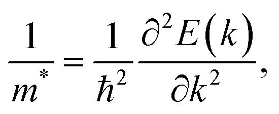 where E(k) is the eigenvalue of energy band around the VBM or the CBM. ħ and k are the reduced Planck constant and wave vector, respectively. The calculated results are listed in Table S1 in the ESI.† As shown in Table S1 (ESI†), the electron effective masses along the X–Γ, X–R and X–M directions are 3.86me, 0.94me and 0.94me, respectively, and the hole effective masses are 1.23me, 1.02me and 3.35me along the R–X, R–Γ and R–M directions, respectively. Our calculated results are in line with previous theoretical study.41 It should be noted that the average hole effective mass is lighter than that of p-type TCM CuAlO2 (10.0me),13,60 which is ascribed to the more dispersive and the higher position of the S_3p orbital compared to that of the O_2p orbital.
 | ||
| Fig. 1 Unit cell of Cu3TaS4 (a). The unit cell of Cu3TaS4 viewed from the (100) direction (b). The 2 × 2 × 2 supercell of Cu3TaS4 (c). The 2 × 2 × 2 supercell of Cu3TaS4 with a Cui (marked by a red dotted circle) in the empty “channel”(d). | ||
 | ||
| Fig. 2 The band structure of Cu3TaS4 with (grey line) and without (red line) the SOC effect (a). The VBM is set to zero. The total density of states (b) and partial density of states of Cu (c), Ta (d) and S (e) atoms and COOPs between the Cu-d and S-p states (f) and the Ta-d and S-p states (g), respectively. The squares of the dipole transition matrix elements between the highest valence band and the lowest conduction band at various k points (h). | ||
3.2 Optical properties of Cu3TaS4
To evaluate the optical transparency of Cu3TaS4, the optical properties, such as absorption coefficient, reflectivity and optical conductivity, are calculated. The details of the optical property calculations are presented in the ESI.† One can note that the optical band gap is larger than that of the electronic band gap, which is ascribed to the indirect band gap character of Cu3TaS4. To further clarify the reason that the optical band gap of Cu3TaS4 is larger than its electronic band gap, we also calculate the squares of the dipole transition matrix elements,61,62P2, at various k points as shown in Fig. 2(h). It is clearly shown that the calculated value of P2 at the X point is close to zero, indicating that the optical transition between the highest valence band and the lowest conduction band at the X point is forbidden. However, the calculated value of P2 at the R point is greater than zero, indicating that the optical transition between the highest valence band and the lowest conduction band at the R point is allowed. The energy difference between the highest valence band and the lowest conduction band at the R point corresponds to the threshold of the absorption coefficient of Cu3TaS4, as shown in Fig. 3(a). Therefore, the optical band gap of Cu3TaS4 is larger than its electronic band gap. Because of the wide optical band gap, the optical absorption is hardly observed in the visible light region, indicating that the visible light can easily pass through the Cu3TaS4 film. Furthermore, the optical transmittance of Cu3TaS4 is also calculated as a function of film thickness based on the following eqn:63| T(ω) = (1 − R(ω)e−α(ω)t). | (1) |
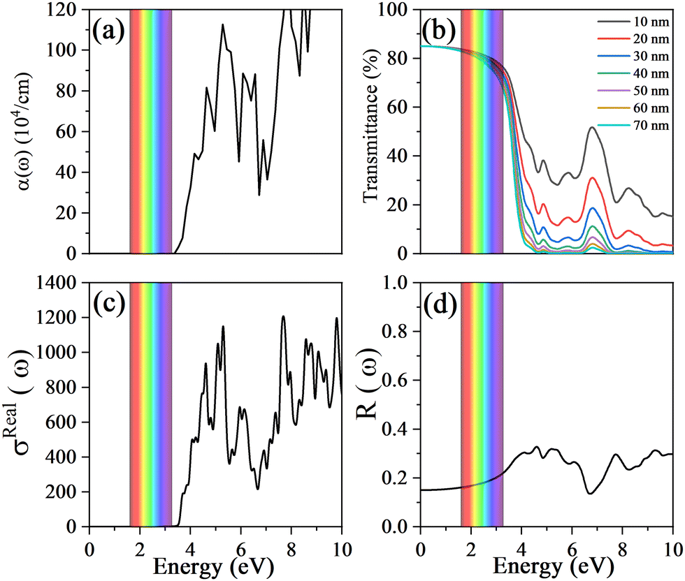 | ||
| Fig. 3 The absorption coefficient (a), the optical transmittance as a function of film thickness (b), the optical conductivity (c) and the reflectivity (d) of Cu3TaS4. | ||
3.3 Defect properties of Cu3TaS4
| 3ΔμCu + ΔμTa+ 4ΔμS = ΔH(Cu3TaS4) = −5.97 eV. | (2) |
In addition, to avoid the formation of element solids and binary or ternary competing phases, ΔμCu, ΔμTa, and ΔμS should be satisfied as the following:
| ΔμCu ≤ 0, ΔμTa ≤ 0, ΔμS ≤ 0. | (3) |
| 2ΔμCu + ΔμS ≤ ΔH(Cu2S) = −0.80 eV; | (4) |
| 2ΔμCu + 3ΔμS ≤ ΔH(Cu2S3) = −1.08 eV; | (5) |
| 7ΔμCu + 4ΔμS ≤ ΔH(Cu7S4) = −2.99 eV; | (6) |
| ΔμCu + ΔμS ≤ ΔH(CuS) = −0.50 eV; | (7) |
| ΔμCu + ΔμTa + 2ΔμS ≤ ΔH(CuTaS2) = −3.73 eV; | (8) |
| ΔμCu + ΔμTa + 3ΔμS ≤ ΔH(CuTaS3) = −4.35 eV; | (9) |
| 3ΔμTa + 2ΔμS ≤ ΔH(Ta3S2) = −4.51 eV; | (10) |
| ΔμTa + 2ΔμS ≤ ΔH(TaS2) = −3.53 eV; | (11) |
| ΔμTa + 3ΔμS ≤ ΔH(TaS3) = −3.56 eV; | (12) |
| 2ΔμTa + ΔμS ≤ ΔH(Ta2S) = −2.21 eV; | (13) |
| 6ΔμTa + ΔμS ≤ ΔH(Ta6S) = −2.56 eV; | (14) |
Based on the constraints mentioned above, the shadow area, as depicted in Fig. 4(a), is the allowed range of relative chemical potentials for stable Cu3TaS4. The intrinsic defect formation energies with the charge state q in different chemical environments (i.e. point A to point G) are calculated based on the supercell model. The calculation method is based on the following eqn:65
 | (15) |
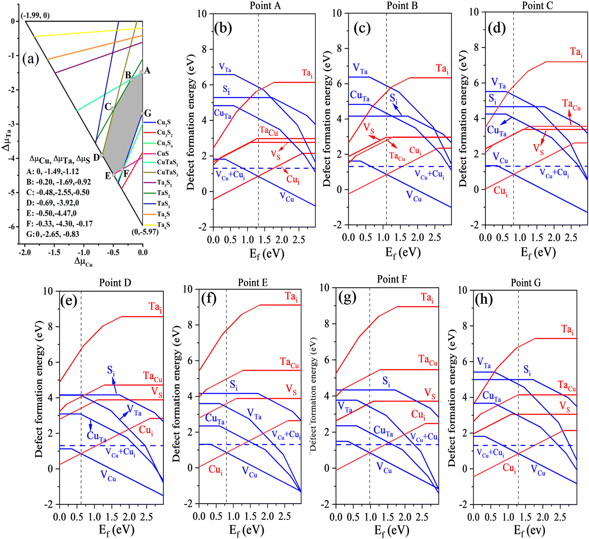 | ||
| Fig. 4 The allowed range of relative chemical potentials for stable Cu3TaS4 (a). The defect formation energies of Cu3TaS4 as a function of the Fermi level under seven extreme chemical potential environments [(point A to point G) (b)–(h)]. The black vertical dotted lines represent the Fermi level at 300 K. | ||
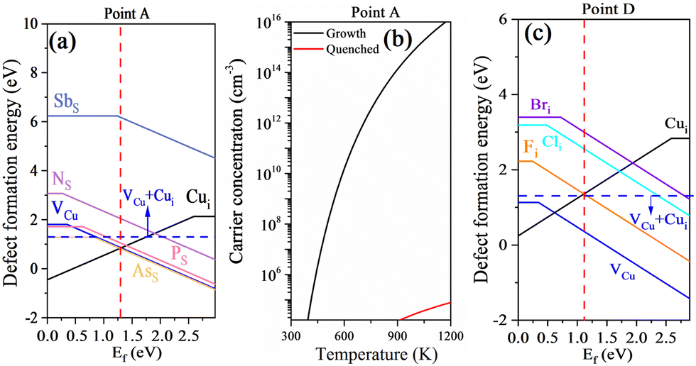
In order to clearly characterize the p-type conductivity of intrinsic Cu3TaS4, the hole concentrations under Cu-rich and Cu-poor conditions are calculated based on the obtained defect properties. While Cu3TaS4 has been experimentally synthesized, the adopted preparation methods correspond to thermodynamic equilibrium growth processes.36,49 Recently, the non-equilibrium growth process has been utilized in both theoretical and experimental studies.69–72 The non-equilibrium growth process involves high-temperature synthesis of the sample followed by rapid quenching to room temperature. Samples fabricated via this method retain the defect density established during high-temperature growth, thereby resulting in enhanced electrical conductivity. Here, the model associated with the high-temperature growth and subsequent quenching processes is applied in our calculations, and the relevant details are presented in the ESI.†Fig. 5(a) and (b) depict the hole concentrations as a function of growth temperature. One can note that the hole concentration is rapidly increased to 1 × 1016 cm−3 after increasing the growth temperature to 1200 K under Cu-rich conditions (point A), as shown in Fig. 5(a). Generally, high temperature is widely used to prepare a defective sample and after sample preparation it is utilized at room temperature. After quenching to room temperature, the Fermi level is pinned in the middle of the band gap and therefore the hole concentration is reduced to 1 × 1012 cm−3, which is mainly ascribed to the compensation of the n-type defect Cui. In the case of the Cu-poor conditions (point D), the hole concentration reaches 5 × 1018 cm−3 when the growth temperature is increased to 1200 K, as shown in Fig. 5(b). However, after quenching to room temperature, the hole concentration is reduced near 1 × 1015 cm−3, which is significantly lower than that of commercialized n-type TCMs. The low hole concentration under Cu-poor conditions is mainly caused by the compensation of the donor defect Cui. To further assess the p-type conductivity of the intrinsic Cu3TaS4, the carrier mobility and the bipolar Seebeck coefficient are also calculated. It is worth noting that the carrier concentration should be given after using the AMSET code. Based on the calculated results, the hole concentration of intrinsic Cu3TaS4 under Cu-poor conditions was estimated to 1.00 × 1015 cm−3. However, the electron concentration of the intrinsic Cu3TaS4 could not be determined due to its p-type conductivity. We therefore estimated the electron concentration of intrinsic Cu3TaS4 based on the detailed balanced theory. The details of electron concentration calculations are presented in the ESI.† The calculated carrier mobility and the bipolar Seebeck coefficient are listed in Table S1 (ESI†). From Table S1 (ESI†), one can conclude that the intrinsic Cu3TaS4 with p-type conductivity has high hole mobility comparing with that of n-type. The calculated hole mobility is lower than that of the previous theoretical study41 using the deformation theory. This discrepancy is attributed to the distinct scattering mechanisms considered in our work. One can note that the Seebeck coefficient of n-type is slightly higher than that of the p-type as shown in Table S1 (ESI†), which is attributed to the inverse relationship between the Seebeck coefficient and carrier concentration. Although the n-type conductivity exhibits a large Seebeck coefficient, the hole concentration exceeding the electron concentration guarantees the p-type conductivity of intrinsic Cu3TaS4. Furthermore, both experimental studies35,36 and our calculation results confirm the p-type conductivity of Cu3TaS4. This is attributed to its suitable hole mobility and lowest defect formation energy of VCu under Cu-poor conditions. In addition, since the growth temperature is increased to 1200 K, it is essential to evaluate the stability of the sample under high temperature. We therefore employ the AIMD simulation to calculate the thermal stabilities at 300 K and 1200 K, respectively. The calculated results are depicted in Fig. S5 (ESI†). It is found that huge energy variations are hardly observed at both 300 K and 1200 K from 0 ps to 10 ps, indicating the thermal stabilities of the sample.
 | ||
| Fig. 5 The hole concentration of intrinsic Cu3TaS4 as a function of growth temperature under Cu-rich (a) and Cu-poor conditions (b), respectively. | ||
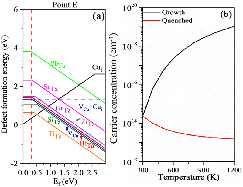 | ||
| Fig. 6 The defect formation energies (a) of p-type doping at the Ta site as a function of the Fermi level at point E. The red vertical dotted line represents the Fermi level at 300 K with TiTa. The hole concentration as a function of growth temperature with TiTa at point E (b). | ||
 | ||
| Fig. 7 The defect formation energies (a) of p-type doping at the S site at point A as a function of the Fermi level. The hole concentration with AsS as a function of growth temperature at point A (b). The defect formation energies of interstitial defects at point D as a function of the Fermi level (c). The red vertical dotted lines are the Fermi level at 300 K. | ||
4. Outlook
Based on the calculated defect properties, the p-type conductivities both from the intrinsic p-type defect VCu and the extrinsic p-type defects (i.e. TiTa doping and AsS doping) can be compensated by the n-type defect Cui. To mitigate the strong compensation effect of the n-type defect Cui and achieve good p-type conductivity, a theoretical strategy recently applied to another p-type transparent conductive material, γ-CuI, is worth exploring.71 Specifically, Matsuzaki et al. introduced alkali metal cations such as Na+, K+, Cs+, and Rb+, all of which have ionic radii larger than that of Cu+, into the interstitial sites of γ-CuI, which lead to the creation of shallow p-type acceptor complexes in association with the surrounding intrinsic defects of γ-CuI. Because of the relatively large ionic radius of Cs+, when Cs+ is incorporated into γ-CuI, two p-type defect complexes serving as shallow acceptors, namely Csi-3VCu-VI and Csi-4VCu-VI, are formed.73 Based on measurements of doped γ-CuI single-crystalline bulks and polycrystalline films, they extend the controllable range of the hole concentration to 1013–1019 cm−3, and the modification of p-type conductivity by defect complexes is supported by first-principles calculations.73 Inspired by this work, future theoretical and experimental studies could attempt to introduce cations with large ionic radii, such as Na+, K+, Rb+, and Cs+, into the empty “channel” of Cu3TaS4 crystal. It is anticipated that the introduced cations will form defect complexes with the adjacent VCu. Subsequently, these defect complexes can act as shallow acceptors, thereby alleviating the compensation effect caused by the n-type defect Cui and enhancing the p-type conductivity of Cu3TaS4. This strategy of large-sized ion doping to form defect complexes offers new insights into reducing the compensation effect of the n-type defect Cui in Cu3TaS4 in future research.5. Conclusions
In summary, based on the first-principles calculations, we demonstrated that Cu3TaS4 is an indirect band gap semiconductor with an electronic band gap of 2.97 eV. The calculated optical properties indicate that Cu3TaS4 exhibits high optical transmittance in the visible light region. Moreover, the results also indicate that the intrinsic Cu3TaS4 exhibits p-type conductivity owing to the low defect formation energy of VCu under Cu-poor conditions. Although the intrinsic Cu3TaS4 exhibits high transparency and p-type conductivity, the hole concentration of the intrinsic Cu3TaS4 only reached 1 × 1015 cm−3 under Cu-poor conditions at room temperature. The low hole concentration and poor p-type conductivity are ascribed to the strong compensation effect of the n-type defect Cui. The ease of formation of the Cui is ascribed to the existence of the empty “channel” along the (100) direction in the Cu3TaS4 crystal. In addition, even after applying two different p-type doping strategies, due to the strong compensating effect of the n-type defect Cui, almost no increase in hole concentrations is observed in the doped samples compared to the intrinsic Cu3TaS4. Therefore, it can be concluded that the empty “channel” in the Cu3TaS4 crystal facilitates the formation of Cui, which leads to the strong compensation effect of the p-type defects, further making it difficult to achieve high hole concentrations and excellent p-type conductivity in Cu3TaS4. To overcome the compensation effect of the n-type defect Cui and obtain ideal p-type conductivity of Cu3TaS4, the introduction of the shallow acceptor defect complex is suggested in the future experimental and theoretical studies.Author contributions
Y. Xue: calculation, data analysis, and writing – original draft; Z. Zhuo: investigation and data analysis; C. Lin: calculation and data analysis; D. Huang: conceptualization, calculation, investigation, data analysis, writing – review, and supervision.Data availability
The data that support the findings of this study are available from the corresponding author upon reasonable request.Conflicts of interest
There are no conflicts to declare.Acknowledgements
This work was financially supported by the Natural Science Foundation of Guangxi Province (grant no. ZY23055002 and 2025GXNSFAA069368), the National Natural Science Foundation of China (grant no. 61964002), and the Opening Project of Guangxi Key Laboratory of Precision Navigation Technology and Application, Guilin University of Electronic Technology (no. DH202316). We acknowledge the supercomputer resources from the National High-Performance Computing Center Nanning Branch.References
- D. S. Hecht, L. Hu and G. Irvin, Emerging transparent electrodes based on thin films of carbon nanotubes, graphene, and metallic nanostructures, Adv. Mater., 2011, 23, 1482–1513 CrossRef CAS PubMed.
- J. Miao and T. Fan, Flexible and stretchable transparent conductive graphene-based electrodes for emerging wearable electronics, Carbon, 2023, 202, 495–527 CrossRef CAS.
- G. Wang, Y. N. Du, P. Huang, Z. F. Qian, P. Zhang and S.-H. Wei, Design of Intrinsic Transparent Conductors from a Synergetic Effect of Symmetry and Spatial-Distribution Forbidden Transitions, Phys. Rev. Lett., 2025, 134, 036401 CrossRef CAS PubMed.
- S. K. Maurya, H. R. Galvan, G. Gautam and X. Xu, Recent progress in transparent conductive materials for photovoltaics, Energies, 2022, 15, 8698 CrossRef CAS.
- R. Kormath Madam Raghupathy, H. Wiebeler, T. D. Kühne, C. Felser and H. Mirhosseini, Database screening of ternary chalcogenides for p-type transparent conductors, Chem. Mater., 2018, 30, 6794–6800 CrossRef CAS.
- T. Isono, T. Fukuda, K. Nakagawa, R. Usui, R. Satoh, E. Morinaga and Y. Mihara, Highly conductive SnO2 thin films for flat-panel displays, J. Soc. Inf. Display, 2007, 15, 161–166 CrossRef CAS.
- K. Nomura, H. Ohta, A. Takagi, T. Kamiya, M. Hirano and H. Hosono, Room-temperature fabrication of transparent flexible thin-film transistors using amorphous oxide semiconductors, Nature, 2004, 432, 488–492 CrossRef CAS PubMed.
- T. Huang, C. Mo, M. Cui, M. Li, P. Ji, H. Tan, X. Zhang, L. Zhuge and X. Wu, Ion behavior impact on ITO thin film fabrication via DC magnetron sputtering with external anode, Vacuum, 2024, 221, 112848 CrossRef CAS.
- T. Koskinen, R. Raju, I. Tittonen and C. Kauppinen, Grass-like alumina enhances transmittance and electrical conductivity of atomic layer deposited Al-doped ZnO for thermoelectric and TCO applications, Appl. Phys. Lett., 2023, 123, 011902 CrossRef CAS.
- S. H. Park, Y.-K. Oh, Y.-J. Lim, S. Z. Chen, S.-J. Lee and H.-K. Kim, Thermally stable and transparent F-doped SnO2 (FTO)/Ag/FTO films for transparent thin film heaters used in automobiles, Ceram. Int., 2023, 49, 2419–2426 CrossRef CAS.
- C. Niu, Carbon nanotube transparent conducting films, MRS Bull., 2011, 36, 766–773 CrossRef CAS.
- T. Minami, Transparent conducting oxide semiconductors for transparent electrodes, Semicond. Sci. Technol., 2005, 20, S35 CrossRef CAS.
- Y. Youn, M. Lee, D. Kim, J. K. Jeong, Y. Kang and S. Han, Large-scale computational identification of p-type oxide semiconductors by hierarchical screening, Chem. Mater., 2019, 31, 5475–5483 CrossRef CAS.
- A. Kudo, H. Yanagi, H. Hosono and H. Kawazoe, SrCu2O2: a p-type conductive oxide with wide band gap, Appl. Phys. Lett., 1998, 73, 220–222 CrossRef CAS.
- X. Nie, S.-H. Wei and S. B. Zhang, Bipolar doping and band-gap anomalies in delafossite transparent conductive oxides, Phys. Rev. Lett., 2002, 88, 066405 CrossRef PubMed.
- K. H. L. Zhang, K. Xi, M. G. Blamire and R. G. Egdell, P-type transparent conducting oxides, J. Phys.: Condens. Matter, 2016, 28, 383002 CrossRef PubMed.
- H. Kawazoe, M. Yasukawa, H. Hyodo, M. Kurita, H. Yanagi and H. Hosono, P-type electrical conduction in transparent thin films of CuAlO2, Nature, 1997, 389, 939–942 CrossRef CAS.
- A. Ananchuensook, I. Chatratin, A. Janotti, T. Watcharatharapong, J. T-Thienprasert, A. Boonchun, S. Jungthawan and P. Reunchan, Hydrogen passivation of acceptor defects in delafossite CuMO2 (M = Al, Ga, In): insights for enhanced p-type conductivity, J. Appl. Phys., 2024, 135, 185705 CrossRef CAS.
- F. Veron, I. Pasquet, Y. Thimont and A. Barnabé, and Ph. Tailhades, Improved performance of transparent p-type conductors CuCrO2:Mg delafossite thin films through easy and low cost laser annealing, Mater. Lett., 2022, 313, 131795 CrossRef CAS.
- C. Esthan, B. G. Nair, A. Surya Mary, J. A. Joseph, L. M. Joseph, R. Jacob, V. K. Shinoj and R. R. Philip, Transparent heterojunctions of Cu-based delafossites n-CuInO2/p-CuGaO2 by reactive evaporation method for transparent electronic applications, Vacuum, 2022, 197, 110808 CrossRef CAS.
- H. Gao, X. Zeng, Q. Guo, Z. Yang, Y. Deng, H. Li and D. Xiong, P-type transparent conducting characteristics of delafossite Ca doped CuScO2 prepared by hydrothermal synthesis, Dalton Trans., 2021, 50, 5262–5268 RSC.
- M. Zhong, W. Zeng, F.-S. Liu, D.-H. Fan, B. Tang and Q.-J. Liu, Screening criteria for high-performance p-type transparent conducting materials and their applications, Mater. Today Phys., 2022, 22, 100583 CrossRef CAS.
- R. Woods-Robinson, M. Morales-Masis, G. Hautier and A. Crovetto, From Design to Device: Challenges and Opportunities in Computational Discovery of p-Type Transparent Conductors, PRX Energy, 2024, 3, 031001 CrossRef.
- P. P. Murmu, M. Markwitz, S. V. Chong, N. Malone, T. Mori, H. Vyas, L. J. Kennedy, S. Rubanov, C. I. Sathish, J. Yi and J. V. Kennedy, Defect and dopant complex mediated high power factor in transparent selenium-doped copper iodide thin films, Mater. Today Energy, 2024, 44, 101639 CrossRef CAS.
- Q. Sun, A. Sadhu, S. Lie and L. H. Wong, Critical review of Cu-based hole transport materials for perovskite solar cells: from theoretical insights to experimental validation, Adv. Mater., 2024, 36, 2402412 CrossRef CAS PubMed.
- M. Benaadad, B. Gul, M. S. Khan and A. Nafidi, Exploring the electronic, optical, and thermometric properties of novel AlCuX2 (X = S, Se, Te) semiconductors: a first-principles study, J. Mater. Sci., 2023, 58, 7362–7379 CrossRef CAS.
- G. Gao, K. Li, L. Yang, F. Xia, L. Xu, J. Han, H. Gong and J. Zhu, 1.37 × 10² S cm−1 p-type conductivity LaCuOS films with a very wide optical transparency window of 400–6000 nm, Mater. Today Phys., 2023, 35, 101089 CrossRef CAS.
- A. Krishnapriyan, P. T. Barton, M. Miao and R. Seshadri, First-principles study of band alignments in the p-type hosts BaM2X2 (M = Cu, Ag; X = S, Se), J. Phys.: Condens. Matter, 2014, 26, 155802 CrossRef.
- Y. Wang, M. Liu, F. Huang, L. Chen, H. Li, X. Lin, W. Wang and Y. Xia, Solution-processed p-type transparent conducting BaCu2S2 thin film, Chem. Mater., 2007, 19, 3102–3104 CrossRef CAS.
- A. Zakutayev, J. Tate and G. Schneider, Defect physics of BaCuChF(Ch = S, Se, Te) p-type transparent conductors, Phys. Rev. B: Condens. Matter Mater. Phys., 2010, 82, 195204 CrossRef.
- A. N. Fioretti and M. Morales-Masis, Bridging the p-type transparent conductive materials gap: synthesis approaches for disperse valence band materials, J. Photon. Energy, 2020, 10, 1 Search PubMed.
- D. Huang, Y.-J. Zhao, R.-Y. Tian, D.-H. Chen, J.-J. Nie, X.-H. Cai and C.-M. Yao, First-principles study of Be doped CuAlS2 for p-type transparent conductive materials, J. Appl. Phys., 2011, 109, 113714 CrossRef.
- M. Li, N. Wang, S. Zhang, J. Hu, H. Xiao, H. Gong, Z. Liu, L. Qiao and X. Zu, A review of the properties, synthesis and applications of lanthanum copper oxychalcogenides, J. Phys. D: Appl. Phys., 2022, 55, 273002 CrossRef.
- K. Rodríguez-Rosales, J. Cruz-Gómez, J. G. Quiñones-Galván, M. de la, L. Olvera, J. Santos-Cruz, G. Contreras-Puente, M. Meléndez-Lira and F. de Moure-Flores, p-Type LaCuOS films grown by PLD using a quaternary target fabricated by a two-step solid-state reaction/sulfurization process, Mater. Sci. Eng., B, 2024, 300, 117063 CrossRef.
- J. Tate, P. F. Newhouse, R. Kykyneshi, P. A. Hersh, J. Kinney, D. H. McIntyre and D. A. Keszler, Chalcogen-based transparent conductors, Thin Solid Films, 2008, 516, 5795–5799 CrossRef CAS.
- P. F. Newhouse, P. A. Hersh, A. Zakutayev, A. Richard, H. A. S. Platt, D. A. Keszler and J. Tate, Thin film preparation and characterization of wide band gap Cu3TaQ4 (Q = S or Se) p-type semiconductors, Thin Solid Films, 2009, 517, 2473–2476 CrossRef CAS.
- N. Zhang, X. Liu, D. B. K. Lim and H. Gong, A New Highly conductive direct gap p-type semiconductor La1−xCuOs for dual applications: transparent electronics and thermoelectricity, ACS Appl. Mater. Interfaces, 2020, 12, 6090–6096 CrossRef CAS PubMed.
- M. Yang, Y. Wang, G. Li, Z. Shi and Q. Zhang, Zn-doped CuAlS2 transparent p-type conductive thin films deposited by pulsed plasma deposition, J. Vac. Sci. Technol., A, 2009, 27, 1316–1319 CrossRef CAS.
- S. Ikeda, N. Aono, A. Iwase, H. Kobayashi and A. Kudo, Cu3MS4 (M = V, Nb, Ta) and its Solid Solutions with Sulvanite Structure for Photocatalytic and Photoelectrochemical H2 Evolution under Visible-Light Irradiation, ChemSusChem, 2019, 12, 1977–1983 CrossRef CAS PubMed.
- A. B. Kehoe, D. O. Scanlon and G. W. Watson, The electronic structure of sulvanite structured semiconductors Cu3MCh4 (M = V, Nb, Ta; Ch = S, Se, Te): prospects for optoelectronic applications, J. Mater. Chem. C, 2015, 3, 12236–12244 RSC.
- Y. Li, M. Wu, T. Zhang, X. Qi, G. Ming, G. Wang, X. Quan and D. Yang, Natural sulvanite Cu3MX4 (M = Nb, Ta; X = S, Se): promising visible-light photocatalysts for water splitting, Comput. Mater. Sci., 2019, 165, 137–143 CrossRef CAS.
- M. Liu, C.-Y. Lai, C.-Y. Chang and D. R. Radu, Solution-Based Synthesis of Sulvanite Cu3TaS4 and Cu3TaSe4 Nanocrystals, Crystals, 2021, 11, 51 CrossRef CAS.
- A. Haque, S. Ershadrad, T. Devaiah Chonamada, D. Saha, B. Sanyal and P. K. Santra, Vacancy assisted growth of copper tantalum sulfide nanocrystals, J. Mater. Chem. A, 2022, 10, 19925–19934 RSC.
- R. Prado-Rivera, C.-Y. Chang, M. Liu, C.-Y. Lai and D. R. Radu, Sulvanites: The Promise at the Nanoscale, Nanomaterials, 2021, 11, 823 CrossRef CAS PubMed.
- W. F. Espinosa-García, G. M. Dalpian and J. M. Osorio-Guillén, Intrinsic defects in sulvanite compounds: the case of transparent Cu3TaS4 and absorbing Cu3VSe4, J. Alloys Compd., 2023, 969, 172264 CrossRef.
- G. Kresse and J. Furthmüller, Efficiency of ab-initio total energy calculations for metals and semiconductors using a plane-wave basis set, Comput. Mater. Sci., 1996, 6, 15–50 CrossRef CAS.
- G. Kresse and D. Joubert, From ultrasoft pseudopotentials to the projector augmented-wave method, Phys. Rev. B: Condens. Matter Mater. Phys., 1999, 59, 1758–1775 CrossRef CAS.
- J. Heyd, J. E. Peralta, G. E. Scuseria and R. L. Martin, Energy band gaps and lattice parameters evaluated with the Heyd–Scuseria–Ernzerhof screened hybrid functional, J. Chem. Phys., 2005, 123, 174101 CrossRef PubMed.
- G. E. Delgado, J. E. Contreras, A. J. Mora, S. Durán, M. Muñoz and P. Grima-Gallardo, Structure refinement of the semiconducting compound Cu3TaS4 from X-Ray powder diffraction data, Acta Phys. Pol. A, 2011, 120, 468–472 CrossRef CAS.
- H. J. Monkhorst and J. D. Pack, Special points for Brillouin-zone integrations, Phys. Rev. B: Condens. Matter Mater. Phys., 1976, 13, 5188–5192 CrossRef.
- A. G. Squires, D. O. Scanlon and B. J. Morgan, PY-SC-FERMI: self-consistent Fermi energies and defect concentrations from electronic structure calculations, JOSS, 2023, 8, 4962 CrossRef.
- R. N. Barnett and U. Landman, Born–Oppenheimer molecular-dynamics simulations of finite systems: structure and dynamics of (H2O)2, Phys. Rev. B: Condens. Matter Mater. Phys., 1993, 48, 2081–2097 CrossRef CAS PubMed.
- J. P. Perdew, K. Burke and M. Ernzerhof, Generalized gradient approximation made simple, Phys. Rev. Lett., 1996, 77, 3865–3868 CrossRef CAS PubMed.
- A. M. Ganose, J. Park, A. Faghaninia, R. Woods-Robinson, K. A. Persson and A. Jain, Efficient calculation of carrier scattering rates from first principles, Nat. Commun., 2021, 12, 2222 CrossRef CAS PubMed.
- H. Arribart, B. Sapoval, O. Gorochov and N. LeNagard, Fast ion transport at room temperature in the mixed conductor Cu3VS4, Solid State Commun., 1978, 26, 435–439 CrossRef CAS.
- H. Arribart and B. Sapoval, Theory of mixed conduction due to cationic interstitials in the p-type semiconductor Cu3VS4, Electrochim. Acta, 1979, 24, 751–754 CrossRef CAS.
- D. M. Schleich and M. Rosso, Li+ insertion studies in Cu3VS4, Solid State Ionics, 1981, 5, 383–385 CrossRef CAS.
- S. Maintz, V. L. Deringer, A. L. Tchougréeff and R. Dronskowski, LOBSTER: a tool to extract chemical bonding from plane-wave based DFT, J. Comput. Chem., 2016, 37, 1030–1035 CrossRef CAS PubMed.
- D. Huang, R.-Y. Tian, Y.-J. Zhao, J.-J. Nie, X.-H. Cai and C.-M. Yao, First-principles study of CuAlS2 for p-type transparent conductive materials, J. Phys. D: Appl. Phys., 2010, 43, 395405 CrossRef.
- G. Trimarchi, H. Peng, J. Im, A. J. Freeman, V. Cloet, A. Raw, K. R. Poeppelmeier, K. Biswas, S. Lany and A. Zunger, Using design principles to systematically plan the synthesis of hole-conducting transparent oxides: Cu3VO4 and Ag3VO4 as a case study, Phys. Rev. B: Condens. Matter Mater. Phys., 2011, 84, 165116 CrossRef.
- V. Wang, N. Xu, J. C. Liu, G. Tang and W.-T. Geng, VASPKIT: a user-friendly interface facilitating high-throughput computing and analysis using vasp code, Comput. Phys. Commun., 2021, 267, 108033 CrossRef CAS.
- A. E. Maughan, A. M. Ganose, M. M. Bordelon, E. M. Miller, D. O. Scanlon and J. R. Neilson, Defect tolerance to intolerance in the vacancy-ordered double perovskite semiconductors Cs2SnI6 and Cs2TeI6, J. Am. Chem. Soc., 2016, 138, 8453–8464 CrossRef CAS PubMed.
- G. Brunin, F. Ricci, V.-A. Ha, G.-M. Rignanese and G. Hautier, Transparent conducting materials discovery using high-throughput computing, npj Comput. Mater., 2019, 5, 63 CrossRef.
- S. B. Zhang, S.-H. Wei and A. Zunger, Intrinsic n-type versus p-type doping asymmetry and the defect physics of ZnO, Phys. Rev. B: Condens. Matter Mater. Phys., 2001, 63, 075205 CrossRef.
- C. Freysoldt, B. Grabowski, T. Hickel, J. Neugebauer, G. Kresse, A. Janotti and C. G. Van De Walle, First-principles calculations for point defects in solids, Rev. Mod. Phys., 2014, 86, 253–305 CrossRef.
- Y. Gai, J. Li, S.-S. Li, J.-B. Xia and S.-H. Wei, Design of narrow-gap TiO2: a passivated codoping approach for enhanced photoelectrochemical activity, Phys. Rev. Lett., 2009, 102, 036402 CrossRef PubMed.
- W.-J. Yin, H. Tang, S.-H. Wei, M. M. Al-Jassim, J. Turner and Y. Yan, Band structure engineering of semiconductors for enhanced photoelectrochemical water splitting: the case of TiO2, Phys. Rev. B: Condens. Matter Mater. Phys., 2010, 82, 045106 CrossRef.
- S. Lany and A. Zunger, Accurate prediction of defect properties in density functional supercell calculations, Modell. Simul. Mater. Sci. Eng., 2009, 17, 084002 CrossRef.
- S. W. Fan, Y. Chen and L. Yang, Transparency and p-Type conductivity of BeSe doped with Group VA Atoms: a hybrid functional study, J. Phys. Chem. C, 2022, 126, 19446–19454 CrossRef CAS.
- X. Zhang, C. Lin, X. Guo, Y. Xue, X. Liang, W. Zhou, C. Persson and D. Huang, Delafossite NaYTe2 as a transparent conductive material with bipolar conductivity: a first-principles prediction, J. Phys. Chem. Solids, 2024, 190, 112002 CrossRef CAS.
- L. Ji, S. Lu, Y. Wu, P. Dai, L. Bian, M. Arimochi, T. Watanabe, N. Asaka, M. Uemura, A. Tackeuchi, S. Uchida and H. Yang, Carrier recombination dynamics of MBE grown InGaAsP layers with 1 eV bandgap for quadruple-junction solar cells, Sol. Energy Mater. Sol. Cells, 2014, 127, 1–5 CrossRef CAS.
- M. Wang, A. Debernardi, Y. Berencén, R. Heller, C. Xu, Y. Yuan, Y. Xie, R. Böttger, L. Rebohle, W. Skorupa, M. Helm, S. Prucnal and S. Zhou, Breaking the doping limit in silicon by deep impurities, Phys. Rev. Appl., 2019, 11, 054039 CrossRef CAS.
- K. Matsuzaki, N. Tsunoda, Y. Kumagai, Y. Tang, K. Nomura, F. Oba and H. Hosono, Hole-doping to a Cu(I)-based semiconductor with an isovalent cation: utilizing a complex defect as a shallow acceptor, J. Am. Chem. Soc., 2022, 144, 16572–16578 CrossRef CAS PubMed.
Footnote |
| † Electronic supplementary information (ESI) available. See DOI: https://doi.org/10.1039/d5cp01186h |
| This journal is © the Owner Societies 2025 |