DOI:
10.1039/D4SC01782J
(Edge Article)
Chem. Sci., 2024,
15, 10989-10996
Large negative differential conductance and its transformation in a single radical molecule†
Received
16th March 2024
, Accepted 2nd June 2024
First published on 3rd June 2024
Abstract
The discovery of negative differential conductance (NDC) in a single molecule and mechanism controlling this phenomenon are important for molecular electronics. We investigated the electronic properties of a typical radical molecule 3-carbamoyl-2,2,5,5-tetramethyl-3-pyrrolin-1-yloxy (CTPO) on an Au(111) surface using low-temperature scanning tunneling microscopy (STM) and inelastic electron tunneling spectroscopy. Large NDC was observed in single CTPO molecules at the boundary of the crystal monolayer. The origin of observed NDC is revealed as the inelastic electron–phonon scattering during tunneling, and the strong spatial variation of the NDC over the single molecule illustrates the nature of the localized radical group. In addition, the NDC can be transformed into a positive differential conductance peak by tuning coupling strengths between different tunneling channels. An empirical multi-channel model has been developed to describe the competition between the valley-shaped NDC and peak-shaped positive differential conductance. The unique electronic property and giant conductance change observed in this radical molecule is valuable for designing novel molecular devices in the future.
Introduction
Negative differential conductance (NDC) is one of the critical properties for many important electronic devices. It plays a significant role in design and construction of resonant tunneling diodes,1,2 oscillators,3–5 and other logical circuits.6,7 In normal semiconductor devices, the NDC is achieved by regulating energy levels in adjacent quantum wells. It is known that the NDC can also be achieved in certain types of molecules, in which the system8–10 can be tuned by regulating the alignment between different molecular orbitals of the molecule. These exciting studies present a promising route to create electronic devices with ultimate miniature size at the sub-nanometer scale. With their unique electronic properties, radical molecules are of particular interest for applications in energy storage,11,12 electron spin resonance,13–16 molecular spintronics,17,18 and opto-electronic devices.19,20 However, very few cases of the NDC in the radical molecules have been reported.21–23 Exploring nonlinear electronic properties in single radical molecules, as well as their underlying physical mechanisms, is highly desirable.
In this work, we investigated NDC features in a typical radical molecule 3-carbamoyl-2,2,5,5-tetramethyl-3-pyrrolin-1-yloxy (CTPO) on a metallic Au(111) surface using low-temperature scanning tunneling microscopy (STM). Inelastic electron tunneling spectroscopy was performed to characterize the NDC with sub-molecular spatial resolution. Localized strong NDC was observed in a single molecule at the edge of the crystal monolayer, and first-principle calculations were carried out to understand the electron–phonon interaction between the tunneling electron and phonon of the molecule. The transition from valley-shaped NDC and peak-shaped positive differential conductance (PDC) was achieved by tuning the STM tunneling junction height, and an empirical multi-channel model was proposed to describe the competition phenomena.
Experimental details and theoretical model
The single-crystal Au(111) substrate was prepared by sputtering with argon ions at 0.5 kV and annealing at about 600 °C for several cycles. The CTPO molecule was first degassed at 50 °C over 20 hours and later sublimated at 70 °C for 2 seconds onto the Au(111) surface, which was held at around 100 K, with a base pressure of 5 × 10⁻¹⁰ torr in the vacuum chamber. Measurements were carried out using a custom lab-built low-temperature STM with the sample held at about 8.5 K. A chemical-etched tungsten tip was used in our experiment. To measure the dI/dV tunneling spectroscopy, the sample bias was modulated using a 321 Hz sine wave with a 1 mV peak amplitude, and the measurement was performed using a lock-in amplifier.
A flat and clean surface of Au(111) with well-known herringbone surface reconstruction was obtained. Self-assembled CTPO monolayer flakes with a size of over 20 nm were easily observed on the surface after the sample was cooled to liquid helium temperature, as shown in Fig. 1a. Fig. 1b and c show a set of dI/dV spectra taken in the monolayer, with equal spacing along the red and black lines shown in the inset of Fig. 1a, respectively. A significant increase in conductance was observed at an energy of about ±40–45 meV, which is a typical feature of inelastic electron tunneling spectroscopy (IETS). A small dip at zero bias voltage was also observed in some spectra taken along the red and black arrows, which manifests a Kondo resonance or low-energy phonon excitation. This zero-bias anomaly is not the focus of this work and will be explored in future studies. We tested tens of molecules within the monolayer, using multiple STM tips. The spectra show the same features as that in Fig. 1b and c, without any indication of negative differential conductance.
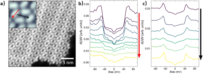 |
| | Fig. 1 STM topograph and spectroscopy of CTPO molecules on the Au(111) surface. (a) Topograph of the CTPO monolayer on the Au(111) surface with tunneling conditions (−0.2 V, 20 pA). Inset is the enlarged image of the area marked with a dashed box on the image. (b) and (c) dI/dV tunneling spectra taken in the monolayer, along red and black arrows depicted in (a). The spectra are offset for clarity. All the spectra were acquired with equal spacing along two lines at a set point (−0.1 V, 0.1 nA) with feedback off. | |
As compared to the elliptical shape of the molecules within the monolayer (defined as type A molecules), the topograph of some molecules at the boundary of the monolayer presents a different, triangular shape (defined as type B molecules), as marked by orange arrows in Fig. 2a. The maximum height of the type B molecules is about 0.02 nm smaller than the height of type A molecules under a scanning set point of (−0.2 V, 20 pA). The inset of Fig. 2a shows the detailed topography of a type B molecule, for which two sets of dI/dV spectra were measured with equal spacing along the two lines as indicated by blue (direction 1) and black (direction 2) arrows, respectively. The general features of these spectra include a dip at zero bias, relatively flat conductance at low bias, step or valley feature at about 40–50 meV, and constant conductance again at higher bias. The step feature is opposite to that for the molecules in the monolayer. In other words, the differential conductance at higher bias is lower than that at the lower bias. Strong NDC appears in some dI/dV spectra taken along direction 1, where the valley feature is most significant. The largest value of the NDC reaches −8 nS, the magnitude of which is 1.6 times the conductance at the low bias voltage. Fig. 2c and d shows the spatial variation in the dI/dV spectra along the two directions. The NDC feature is localized in a certain region of the molecule along direction 1 with its maximum near the outer edge of the type B molecule. The spatial width at half maximum of this NDC feature is about 0.3 nm. Along direction 2, conversely, the valley in the dI/dV spectra drops to negative values in only a few spectra.
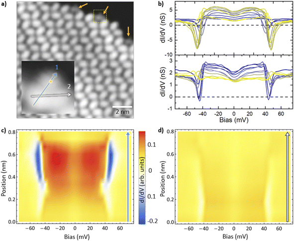 |
| | Fig. 2 NDC in CTPO at the boundary of the monolayer. (a) Typical topograph of the molecules at the edge of the CTPO monolayer. Scanning conditions: 0.2 V, 20 pA. (Inset) Zoomed-in image of a type B molecule. (b) STS spectra taken in a type B molecule. All spectra were acquired with equal spacing on the two lines at a set point (−0.1 V, 0.1 nA) with feedback off. (c) and (d) STS color map as a function of bias voltage and position along direction 1 and direction 2, respectively. | |
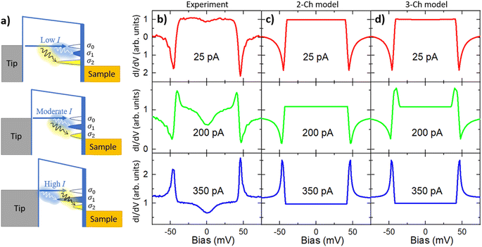
To characterize the properties of the NDC and to understand its mechanism, we investigated the effect of tunneling junction distance on the NDC in such molecules. The STM tip was positioned at the point with maximum NDC, as marked with a star on the inset of Fig. 2a. A series of the dI/dV spectra were measured under different tunneling junction conditions, as shown in Fig. 3. The tunneling current was tuned from 25 pA to 350 pA, corresponding to a decrease in junction distance of about 0.15 nm. The valley feature of the NDC is clearly changed to a positive differential conductance peak when the tunneling current is set higher than 150 pA. In addition, the energy of the positive peak in the spectra is shifted from 34 meV at 150 pA to 45 meV at 350 pA, while the change in the valley position of the NDC is not noticeable.
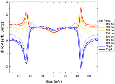 |
| | Fig. 3 Normalized dI/dV spectra taken on a single molecule with various tunneling junction distances. The tunneling set point was changed from 25 pA to 350 pA, with the bias voltage set as −0.1 V. | |
The symmetric valley and peak features in the dI/dV tunneling spectra with respect to the zero bias voltage are typical characteristics of the inelastic scattering of phonon modes in the molecule. When electrons tunnel through the junction with sufficient energy, inelastic scattering can be induced between the electrons and phonon of the molecule, opening an additional tunneling channel. The additional tunneling channel usually creates a step, peak, or valley feature at a threshold bias voltage at both polarities. The step feature is common for simple molecules directly adsorbed on a surface, for which the electron–phonon scattering reaches balance quickly between each tunneling channel and is bias-independent. The peak and valley features, conversely, can be observed if a significant bias-dependent channel occupation exists. Depending on the channel occupation with respect to the bias voltage, as well as conductance of the newly opened channel as compared to the background conductance, the IETS feature can be either a valley-shaped NDC or positive peak, which is sometimes referred to as positive differential conductance (PDC),24–26 which can be described using a two-state model with saturation effects,25 asymmetric coupling,24 or vibration.27
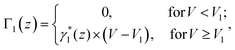
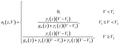
While relative conductance changes have been observed in break junction experiments by tuning the coupling between electrodes and phonon modes of a molecule or atomic chain,28–30 the transition between NDC and PDC in a single nanosystem has never been reported in experimental or theoretical studies. The data shown in Fig. 3 illustrate the competition of electron tunneling between different channels. To describe these competition phenomena, we developed an empirical multi-channel model as follows. We start with two channels: a ground state |m,0> and an excited state |m,1>. The ground state channel contributes a conductance σ0 in the low-energy region (<25 meV), in which the tunneling probability is determined by P0 = Γ0(z)|<tip|He−m|m,0>|2. The coefficient Γ0(z) is constant at a specific tip state and junction height z, and He−m is the Hamiltonian of tip-molecule coupling in the junction. Similarly, the tunneling probability for the excited state can be written as P1 = Γ1(z)|<tip|He−m|m,1>|2, generating a different conductance σ1. The coefficient Γ1(z) has a strong dependence on the bias voltage around the excitation threshold. Here, we adopt a formula similar to that in the previous report:25
| |  | (1) |
where,

is the coefficient for electron phonon coupling (EPC), which depends on the junction distance
z, and
V1 is the excitation voltage threshold. The channel occupation for the ground state can thus be written as
n0 =
P0/(
P0 +
P1) and that for the excited state as
n1 =
P1/(
P0 +
P1). The dependence of
n1 can then be further expressed as a function of the bias voltage and junction distance:
| | 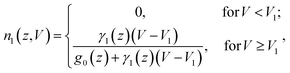 | (2) |
where,
γ1(
z) is the effective electron phonon coupling (EPC) coefficient between the tip and ground state. The general formula of
γi(
z) is
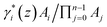
, where
Ai = |<tip|
He−m|
m,
i>|2 and
n is total number of channels. Similarly,
g0(
z) is the effective coupling coefficient between the tip and ground. The general formula of
g0(
z) is

. The total current and differential conductance can now be written as:
| | | I(z,V) = n0(z)Vσ0 + n1(z)Vσ1 | (3) |
| |  | (4) |
The conductance formula (4) can be employed to fit the dI/dV spectra acquired at 25 pA and 350 pA on the CTPO molecules at the boundary of the film, as shown in Fig. 4b. The fitting parameters are: σ1 = 0.2σ0, γ1 = 108g0, V1 = 44 mV for the 25 pA case, and σ1 = 1.2σ0, γ1 = 402g0, V1 = 45 mV for the 350 pA case. A 2 mV full width at half maximum Gaussian window was used to broaden curves. We note again that the dip feature at zero bias is not considered in the model.
 |
| | Fig. 4 Multi-channel model and the differential tunneling spectra. (a) Diagram of three-channel model at different tunneling distances. (b–d) Experimental dI/dV spectra and simulation with the two-channel model and three-channel model, respectively. | |
As expected, the two-channel model works well in low-current and high-current cases, in which only peak-shaped PDC or valley-shaped NDC is observed in the spectra. It, however, fails to reproduce the dI/dV spectra with the PDC and NDC in the case of moderate current. A third channel with a conductance σ2 and excitation threshold voltage V2 is then introduced to the model. The tunneling probability of this channel is  . The occupation of each channel is now written as:
| |  | (5) |
| |  | (6) |
| | | n0(z,V) = 1 − n1(z,V) − n2(z,V) | (7) |
The total current and differential conductance is expressed as:
| | | I(z,V) = n0Vσ0 + n1Vσ1 + n2Vσ2 | (8) |
| |  | (9) |
Using this three-channel model, the dI/dV spectra acquired at 200 pA can be fitted well using following parameters: σ2 = 0.2σ0, γ2 = 47g0, V2 = 46 mV, σ1 = 1.2σ0, γ1 = 65g0, and V1 = 38 mV, as shown in Fig. 4d. It also works well in the other two cases.
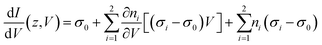
We then fitted all the dI/dV spectra in Fig. 3 using eqn (9). The results are displayed in Fig. 5. The color maps of experimental data and simulation show a clear competition between NDC and PDC features. Excitation energies and EPC coefficients are shown in Fig. 5c and d, respectively. While the variation in the threshold voltage for NDC, V2, is only about 3 mV, the threshold voltage for PDC (V1) shifts by more than 10 mV. The monotonic shift in threshold voltage V1 may come from the Stark effect,31 charging-induced phonon energy shift32 or other possible mechanisms. The EPC coefficients show different tendencies, i.e., γ2 decreases but γ1 increases as the set point current increases. This indicates strong competition between the two excited channels that may originate from atomic interaction or dipole coupling between the tip and phonon modes.33
 |
| | Fig. 5 Influence of tunneling distance on the tunneling spectra. (a) Experimental tunneling spectra under different set points. (b) Simulated tunneling spectra with the three-channel model. Dashed curves are guides for the peak shift. (c) Fitted values of threshold voltages V1 and V2. (d) Normalized coupling coefficients at different set points. | |
Discussion
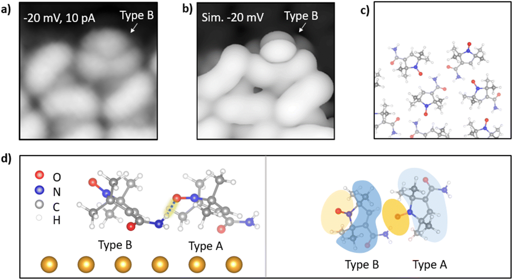
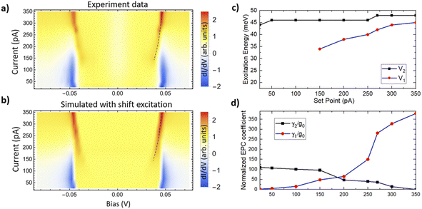
We first discuss the origin of topographical differences between the type A and B molecules. Using a sharp tip and a low bias voltage, we obtained a high-resolution image of the monolayer boundary as depicted in Fig. 6a, in which the type B molecule has a pronounced protrusion. DFT simulation illustrates that this originates from the different adsorption geometries of CTPO at the edge of the monolayer as compared to those within the monolayer. Fig. 6d presents the simulated configuration of the two interacting CTPO molecules as obtained using ab initio molecular dynamics (AIMD) simulation with CP2K34 software. The N–O group of one molecule (right) interacts with the carbamoyl group of the other molecule (left) through a hydrogen bond. On the contrary, the N–O group of the molecule on the left points out freely. The distance between the hydrogen atom and oxygen atom for the hydrogen bond is about 1.84 Å. Due to the hydrogen bond interaction, the oxygen atom in the N–O group of the molecule on the right is lowered by about 1.08 Å in comparison to that of the molecule on the left. This simulated absorption difference makes it easy to identify the right molecule as type A and the left one as type B, considering the different appearances of both the types of molecules in STM topographic images. We also performed a simulation of the STM image based on the balanced structures of AIMD simulations, as shown in Fig. 6b and c, which is consistent with the experimental image in Fig. 6a. It is revealed that two methyl groups on the top of molecule are associated with the long elliptic shape in the topograph, and the pronounced protrusion in the type B molecule is related to the N–O group. This protrusion is much weaker for the type A molecule due to the lowered height of the N–O group. It is thus clear that the spatially resolved NDC excitation shown in Fig. 2 is localized on the position of the N–O group. The details can be seen in ESI.†
 |
| | Fig. 6 High-resolution STM image and DFT simulation for the two types of CTPO molecules. (a) High-resolution STM image of the CTPO molecules at the boundary of the monolayer. The size of the image is 2.08 nm × 2.08 nm. (b) Simulated STM image in comparison to (a). (c) Molecular model corresponding to the simulation. (d) Simulated ball-stick model of the two interacting CTOP molecules on a gold substrate. The dashed line indicates the hydrogen bond. (left) Side view; (right) top view of the two molecules without the Au substrate. | |
We further examined the phonon modes of the CTPO molecule adsorbed on the surface. It is necessary to include the substrate in the calculation, since the phonon modes of the molecules often change after adsorption on a substrate.35–37Fig. 7a shows the phonon modes of both the types of molecules within an energy range from 10 meV to 70 meV. Typical dI/dV spectra are displayed as well for comparison. To identify the phonon modes related to observed spectral features, we focus on the phonon modes that have significant contributions from the vibration of the oxygen atom in the N–O group. Examination of the infrared activity of these phonon modes shows noticeable N–O radical related IR intensity in each mode (see ESI†), implying easy dipole excitation of the N–O group.33,38–41 The symmetry of each IETS channel has also been considered. It has been reported in previous studies29,30 that the conductance change can be associated with the direction of the molecular vibration. The longitudinal phonon mode (vibration along the tunneling direction) often results in a decrease in conductance, while transverse vibration is often associated with an increase in conductance. To distinguish the modes with respect to the vibration direction, we calculated angle θ between the vibration and tunneling directions for each mode, as listed in Fig. 7b. The contribution of each phonon mode to the PDC can then be characterized by the projected vibration amplitude of the oxygen atom along the tunneling direction, i.e., Amp. × sin(θ). For the NDC, it is characterized by Amp. × cos(θ). For the type A molecules, the phonon mode at 42 meV has a strong contribution to the PDC, which is denoted as PA, and there is no mode possessing a similar contribution to the NDC. For the type B molecules, the PDC can be associated with the phonon mode at around 39 meV, which is denoted as PB, and the NDC can be associated with the phonon mode at around 47 meV, denoted as NB. Fig. 7d shows the detailed images of the vibration of the NB and PA modes. It can be seen that the vibration direction of the oxygen atom for the PA mode is transverse, θ = 0.47π. The NB phonon mode, conversely, has a significant component along the tunneling direction, θ = 0.3π. This significant change in the electrical conductivity caused by a slight molecular conformation change and multi-channel competition could be utilized for the regulation of molecular electronic devices in the future. Our experiment demonstrated a significant peak-to-valley ratio in NDC spectra, reaching 2.4 (ESI†) under an operation power of about 1.3 pW. In practice, the radical molecules can be sandwiched between two electrodes with semiconducting spacing layer(s), the thickness of which and the profile of tunneling gap(s) can be controlled by the gate voltage(s), thus generating a similar modulation effect on the NDC.
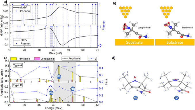 |
| | Fig. 7 NDC- and PDC-related phonon modes. (a) dI/dV spectra with the phonon modes of the type B and type A molecules. (b) Schematic images for the longitudinal and transverse vibrations of the oxygen atom in the N–O group. (c) Vibration amplitude, direction angle, and projected amplitudes of selected phonon modes in the type A and type B molecules. (d) Vibration image of NB (NDC of type B) and PA (PDC of type A) phonon modes, respectively. | |
Summary
To summarize, we observed a strong NDC in certain CTPO molecules on a Au(111) surface using a low-temperature STM and IETS. The localized NDC feature in the dI/dV spectra becomes a PDC peak feature as the junction distance is tuned by about 0.15 nm. The topographical difference between the CTPO molecules at the monolayer center and boundary has been fully investigated with the aid of the AIMD simulation. An empirical multi-channel model has been developed to explain the experimental data and provide insight into the competition between different channels. Although the competition in this study is among the different phonon modes, other types of channel competition are also possible. Significant changes in electrical conductivity properties caused by conformational changes exhibited by the type A and type B molecules have important reference significance for future regulation of molecular structures to achieve controlled electrical conductivity. Our results indicate that the CTPO molecules, as well as other similar molecules, are promising components for the design and fabrication of novel molecular electronic devices in the future.
Data availability
The data that support the discoveries of this paper are available from the corresponding author upon request.
Author contributions
X. T. performed the experiments and the calculations under the supervision of X. L. W. W., H. T., M. W., X. Y., J. Z. and X. S. gave assistances in the experiment. D. H. gave advices in DFT simulation. All authors contributed to the data analysis and the writing of the manuscript.
Conflicts of interest
The authors declare no conflicts of interests.
Acknowledgements
This research is supported by National Science Foundation of China under Grant No. 21961142021, 11774395, 11727902, and 91753136, Beijing Natural Science Foundation under Grant No. 4181003, Strategic Priority Research Program (B) of the Chinese Academy of Sciences, Grant No. XDB30201000. We also express gratitude for the calculation support from the Platform for Data-Driven Computational Materials Discovery, Songshan Lake Materials Laboratory.
References
- K. Ismail, B. Meyerson and P. Wang, Electron resonant tunneling in Si/SiGe double barrier diodes, Appl. Phys. Lett., 1991, 59(8), 973–975 CrossRef CAS
 .
.
- L. Esaki, New phenomenon in narrow germanium p−n junctions, Phys. Rev., 1958, 109(2), 603 CrossRef CAS .
- E. R. Brown, J. Söderström and C. Parker,
et al., Oscillations up to 712 GHz in InAs/AlSb resonant-tunneling diodes, Appl. Phys. Lett., 1991, 58(20), 2291–2293 CrossRef CAS .
-
R. Izumi, S. Suzuki and M. Asada, 1.98 THz resonant-tunneling-diode oscillator with reduced conduction loss by thick antenna electrode, Proceedings of the 2017 42nd International Conference on Infrared, Millimeter, and Terahertz Waves (IRMMW-THz), IEEE, 2017 Search PubMed .
- S. Suzuki, M. Shiraishi and H. Shibayama,
et al., High-power operation of terahertz oscillators with resonant tunneling diodes using impedance-matched antennas and array configuration, IEEE J. Sel. Top. Quantum Electron., 2012, 19(1), 8500108 Search PubMed .
- L. Britnell, R. Gorbachev and A. Geim,
et al., Resonant tunnelling and negative differential conductance in graphene transistors, Nat. Commun., 2013, 4(1), 1794 CrossRef CAS .
- H. Ishikuro and T. Hiramoto, Quantum mechanical effects in the silicon quantum dot in a single-electron transistor, Appl. Phys. Lett., 1997, 71(25), 3691–3693 CrossRef CAS .
- X. W. Tu, G. Mikaelian and W. Ho, Controlling single-molecule negative differential resistance in a double-barrier tunnel junction, Phys. Rev. Lett., 2008, 100(12), 126807 CrossRef CAS .
- M. L. Perrin, R. Frisenda and M. Koole,
et al., Large negative differential conductance in single-molecule break junctions, Nat. Nanotechnol., 2014, 9(10), 830–834 CrossRef CAS .
- G. Kuang, S. Z. Chen and L. Yan,
et al., Negative differential conductance in polyporphyrin oligomers with nonlinear backbones, J. Am. Chem. Soc., 2018, 140(2), 570–573 CrossRef CAS .
- E. P. Tomlinson, M. E. Hay and B. W. Boudouris, Radical Polymers and Their Application to Organic Electronic Devices, Macromolecules, 2014, 47(18), 6145–6158 CrossRef CAS .
- D. A. Wilcox, V. Agarkar and S. Mukherjee,
et al., Stable Radical Materials for Energy Applications, Annu. Rev. Chem. Biomol. Eng., 2018, 9, 83–103 CrossRef .
- A. V. Balatsky, M. Nishijima and Y. Manassen, Electron spin resonance-scanning tunneling microscopy, Adv. Phys., 2012, 61(2), 117–152 CrossRef CAS .
- P. Krukowski, W. Olejniczak and Z. Klusek,
et al., An ESN-STM spectrometer for single spin detection, Measurement, 2010, 43(10), 1495–1502 CrossRef .
- M. Mannini, P. Messina and L. Sorace,
et al., Addressing individual paramagnetic molecules through ESN-STM, Inorg. Chim. Acta, 2007, 360(13), 3837–3842 CrossRef CAS .
- A. V. Balatsky, Y. Manassen and R. Salem, ESR-STM of a single precessing spin: Detection of exchange-based spin noise, Phys. Rev. B: Condens. Matter Mater. Phys., 2002, 66(19), 195416 CrossRef .
- M. Mas-torrent, N. Crivillers and V. Mugnaini,
et al., Organic radicals on surfaces: towards molecular spintronics, J. Mater. Chem., 2009, 19(12), 1691–1695 RSC .
- S. Sanvito, Molecular spintronics, Chem. Soc. Rev., 2011, 40(6), 3336–3355 RSC .
- Q. Peng, A. Obolda and M. Zhang,
et al., Organic light-emitting diodes using a neutral π radical as emitter: the emission from a doublet, Angew. Chem., 2015, 127(24), 7197–7201 CrossRef .
- E. Neier, R. A. Ugarte and N. Rady,
et al., Solution-processed organic light-emitting diodes with emission from a doublet exciton; using (2, 4, 6-trichlorophenyl) methyl as emitter, Org. Electron., 2017, 44, 126–131 CrossRef CAS .
- N. P. Guisinger, M. E. Greene and R. Basu,
et al., Room temperature negative differential resistance through individual organic molecules on silicon surfaces, Nano Lett., 2004, 4(1), 55–59 CrossRef CAS .
- N. Crivillers, M. Paradinas and M. Mas-torrent,
et al., Negative differential resistance (NDR) in similar molecules with distinct redox behaviour, Chem. Commun., 2011, 47(16), 4664–4666 RSC .
- S. Koiry, D. Aswal and B. Jousselme,
et al., Negative differential resistance in electrografted layer of N-(2-(4-diazoniophenyl) ethyl)-N′-hexylnaphthalene-1,8: 4,5-tetracarboxydiimide tetrafluoroborate on Si, Chem. Phys. Lett., 2010, 493(1–3), 135–140 CrossRef CAS .
- A. Halbritter, P. Makk, S. Csonka and G. Mihály, Huge negative differential conductance in Au-H2 molecular nanojunctions, Phys. Rev. B: Condens. Matter Mater. Phys., 2008, 77(7), 075402 CrossRef .
- J. A. Gupta, C. P. Lutz and A. J. Heinrich,
et al., Strongly coverage-dependent excitations of adsorbed molecular hydrogen, Phys. Rev. B: Condens. Matter Mater. Phys., 2005, 71(11), 115416 CrossRef .
- J. Gaudioso, L. J. Lauhon and W. Ho, Vibrationally mediated negative differential resistance in a single molecule, Phys. Rev. Lett., 2000, 85(9), 1918–1921 CrossRef CAS .
- W. H. Thijssen, D. Djukic and A. F. Otte,
et al., Vibrationally induced two-level systems in single-molecule junctions, Phys. Rev. Lett., 2006, 97(22), 226806 CrossRef CAS .
- N. Agraït, C. Untiedt and G. Rubio-bollinger,
et al., Onset of energy dissipation in ballistic atomic wires, Phys. Rev. Lett., 2002, 88(21), 216803 CrossRef .
- D. Djukic, K. S. Thygesen and C. Untiedt,
et al., Stretching dependence of the vibration modes of a single-molecule Pt− H 2− Pt bridge, Phys. Rev. B: Condens. Matter Mater. Phys., 2005, 71(16), 161402 CrossRef .
- R. Ben-zvi, R. Vardimon and T. Yelin,
et al., Electron–vibration interaction in multichannel single-molecule junctions, ACS Nano, 2013, 7(12), 11147–11155 CrossRef CAS .
- J. M. Marr and Z. D. Schultz, Imaging Electric Fields in SERS and TERS Using the Vibrational Stark Effect, J. Phys. Chem. Lett., 2013, 4(19), 3268–3272 CrossRef CAS .
- Y. Li, P. Doak and L. Kronik,
et al., Voltage tuning of vibrational mode energies in single-molecule junctions, Proc. Natl. Acad. Sci. U. S. A., 2014, 111(4), 1282–1287 CrossRef CAS .
- N. Okabayashi, Y. Konda and T. Komeda, Inelastic electron tunneling spectroscopy of an alkanethiol self-assembled monolayer using scanning tunneling microscopy, Phys. Rev. Lett., 2008, 100(21), 217801 CrossRef .
- T. D. Kühne, M. Iannuzzi and B. E. N. M. Del,
et al., CP2K: An electronic structure and molecular dynamics software package - Quickstep: Efficient and accurate electronic structure calculations, J. Chem. Phys., 2020, 152(19), 194103 CrossRef .
- Y. Yao, N. Nijem and J. Li,
et al., Analyzing the frequency shift of physiadsorbed CO 2 in metal organic framework materials, Phys. Rev. B: Condens. Matter Mater. Phys., 2012, 85(6), 064302 CrossRef .
- F. M. Hoffmann, Infrared reflection-absorption spectroscopy of adsorbed molecules, Surf. Sci. Rep., 1983, 3(2–3), 107–192 CrossRef CAS .
-
T. E. Madey and J. R. J. T. Yates, Vibrational spectroscopy of molecules on surfaces, Springer Science & Business Media, 2013 Search PubMed .
- P. Avouris, R. E. Walkup and A. R. Rossi,
et al., Breaking individual chemical bonds via STM-induced excitations, Surf. Sci., 1996, 363(1–3), 368–377 CrossRef CAS .
- G. Binnig, N. Garcia and H. Rohrer, Conductivity sensitivity of inelastic scanning tunneling microscopy, Phys. Rev. B: Condens. Matter Mater. Phys., 1985, 32(2), 1336 CrossRef CAS .
- N. Lorente and M. Persson, Theory of single molecule vibrational spectroscopy and microscopy, Phys. Rev. Lett., 2000, 85(14), 2997–3000 CrossRef CAS .
- K. J. Franke and J. I. Pascual, Effects of electron-vibration coupling in transport through single molecules, J. Phys.: Condens.Matter, 2012, 24(39), 394002 CrossRef .
|
| This journal is © The Royal Society of Chemistry 2024 |
Click here to see how this site uses Cookies. View our privacy policy here. 
 Open Access Article
 This Open Access Article is licensed under a Creative Commons Attribution-Non Commercial 3.0 Unported Licence
 ab,
Wenyu
Wang
ab,
Haitao
Tang
ab,
Muyu
Wang
ab,
Xia
Ye
ab,
Dong
Hao
ab,
Wenyu
Wang
ab,
Haitao
Tang
ab,
Muyu
Wang
ab,
Xia
Ye
ab,
Dong
Hao


 is the coefficient for electron phonon coupling (EPC), which depends on the junction distance z, and V1 is the excitation voltage threshold. The channel occupation for the ground state can thus be written as n0 = P0/(P0 + P1) and that for the excited state as n1 = P1/(P0 + P1). The dependence of n1 can then be further expressed as a function of the bias voltage and junction distance:
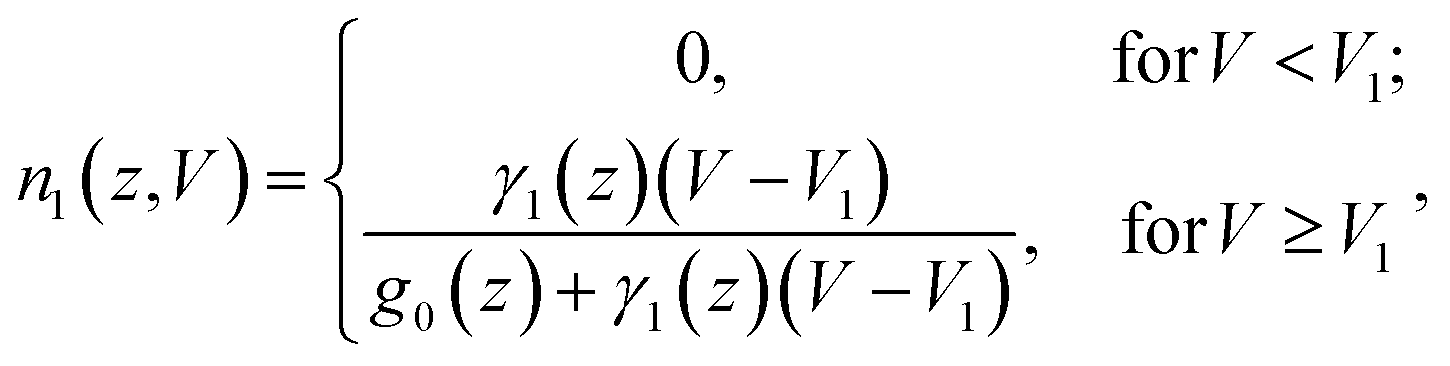
 , where Ai = |<tip|He−m|m,i>|2 and n is total number of channels. Similarly, g0(z) is the effective coupling coefficient between the tip and ground. The general formula of g0(z) is
  . The total current and differential conductance can now be written as:

 . The occupation of each channel is now written as: