
 Open Access Article
 This Open Access Article is licensed under a Creative Commons Attribution-Non Commercial 3.0 Unported Licence
Demonstration of a low power and high-speed graphene/silicon heterojunction near-infrared photodetector†
Min Gyu
Kwon
a,
Cihyun
Kim
b,
Seung-Mo
Kim
b,
Tae Jin
Yoo
b,
Yongsu
Lee
 b,
Hyeon Jun
Hwang
c,
Sanghan
Lee
*a and
Byoung Hun
Lee
*b
b,
Hyeon Jun
Hwang
c,
Sanghan
Lee
*a and
Byoung Hun
Lee
*b
aSchool of Materials Science and Engineering, Gwangju Institute of Science and Technology (GIST), 123, Cheomdangwagi-ro, Buk-gu, Gwangju 61005, Republic of Korea. E-mail: sanghan@gist.ac.kr
bDepartment of Electrical Engineering, Pohang University of Science and Technology (POSTECH), 77, Cheongam-ro, Nam-gu, Pohang-si, Gyeongsangbuk-do 37673, Republic of Korea. E-mail: bhlee1@postech.ac.kr
cDepartment of Semiconductor Engineering, Mokpo National University, 1666, Yeongsan-ro, Cheonggye-myeon, Muan-gun, Jeollanam-do 58554, Republic of Korea
First published on 20th May 2024
Abstract
The structure and process of the graphene/Si heterojunction near-infrared photodetector were optimized to enhance the operating speed limit. The introduction of a well-designed structure improved the rise time from 12.6 μs to 115 ns, albeit at the expense of the responsivity, which decreased from 1.25 A W−1 to 0.56 A W−1. Similarly, the falling time was improved from 38 μs to 288 ns with a sacrifice in responsivity from 1.25 A W−1 to 0.29 A W−1, achieved through the introduction of Ge-induced defect-recombination centers within the well. Through a judicious well design and the introduction of recombination defect centers, the minimum pulse width could be improved from 50.6 μs to 435 ns, facilitating 2 MHz operation. This represents more than 100 times increase compared to previously reported graphene and graphene/Si hybrid photodetectors.
1. Introduction
Near-infrared (NIR) photodetectors find applications in a broad spectrum of uses, including sensors for autonomous driving cars, optical communication and medical instruments. These photodetectors are fabricated using diverse materials such as binary semiconductors such as GaAs, InP, and CdTe,1–4 ternary semiconductors like HgCdTe and InGaAs,5–7 or silicon-based PIN devices.8,9 However, the fabrication process for these photodetectors is intricate and involves multiple costly steps, limiting the broader applications.To address these challenges, many new materials have been actively explored, including various transition-metal dichalcogenides (TMDC),10–12 quantum dots,13,14 and graphene,15–17 with the aim of achieving improved performance and simplified processes. Graphene, a two-dimensional material, has been extensively studied due to wide bandwidth and excellent electrical conductivity.18,19 Nonetheless, the net light absorption rate of graphene is comparatively lower than that of alternative materials, primarily because of its limited absorption volume.20 Furthermore, the high dark current resulting from the absence of a band gap makes graphene less competitive compared to other candidate materials.21
To overcome these challenges, graphene/semiconductor heterojunction photodetectors have been proposed.22–25 This type of photodetector can be manufactured with significantly shorter processing steps, eliminating the need for an expensive epitaxy process. The junction structure can be formed simply by transferring graphene onto the semiconductor substrate. The key advantage of graphene/semiconductor heterojunction photodetectors lies in the unique Fermi level modulation characteristic of graphene, which can be leveraged to reduce dark current and enhance responsivity.24 Wang et al.26 developed a self-powered graphene/Si Schottky junction photodetector that, at zero bias, exhibited a responsivity of 39.5 mA W−1 with a response time of 5.0 μs. Similarly, Scagliotti et al.27 reported a graphene/Si Schottky-junction-based photodetector with an ultrahigh responsivity of 107 A W−1 and a response time of 0.11 ms. While these graphene/Si-heterojunction-based photodetectors show high responsivity, their response times are deemed too slow for many practical applications.
In this study, we illustrate a significant enhancement in the response speed of a graphene/Si heterojunction photodetector in the near-infrared region by restricting the carrier collection volume in the bulk substrate. This improvement is achieved through the addition of an isolated well tub under the graphene/semiconductor junction, coupled with a reduction in the recombination lifetime of residual photocarriers. The introduction of the well structure leads to a reduction in the photoactive volume, resulting in a decrease in responsivity from 1.25 A W−1 to 0.56 A W−1 at 850 nm. However, the rise time of the response signal experiences a substantial improvement, transitioning from 1.26 μs to 115 ns—more than two orders of magnitude faster. This outcome surpasses the previously reported best rise time for a graphene/Si photodetector by at least 2.75 times. Furthermore, through the incorporation of Ge-induced defect-recombination centers, the fall time is also enhanced from 38 μs to 285 ns, enabling 2 MHz operation.
2. Experimental
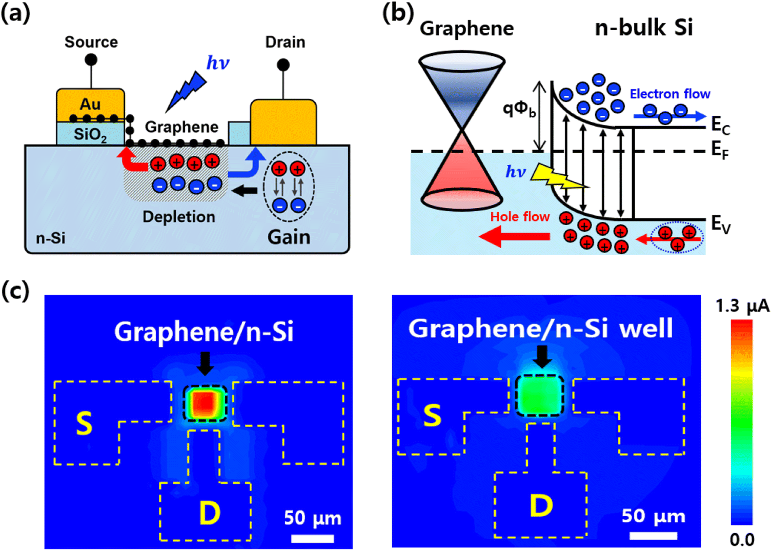
Fig. 1(a) and (b) depict schematic diagrams of the graphene/n-type bulk Si photodetector and graphene/n-Si well-tub/p-type bulk Si photodetectors, respectively. Both devices involve the formation of a junction between graphene and Si, but the graphene/n-Si well-tub/p-Si photodetector features a junction with the n-Si well formed on the p-Si substrate. Fig. 1(c) provides a cross-sectional schematic of the device.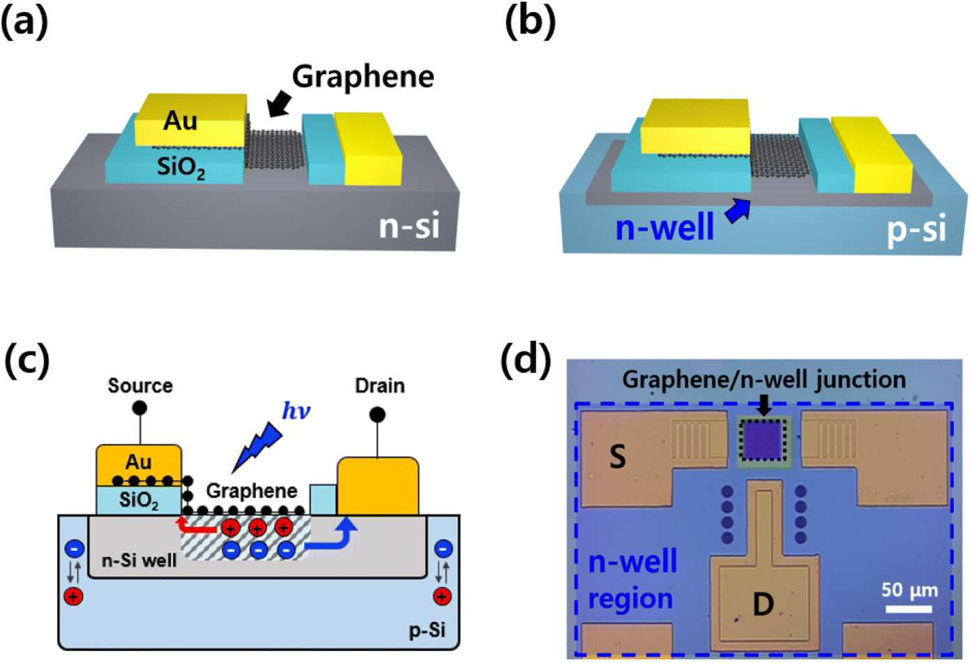 | ||
| Fig. 1 Schematic diagrams of (a) graphene/n-type bulk Si Schottky junction photodetector and (b) graphene/n-Si well-tub/p-Si photodetector. (c) A cross-sectional schematic of the device including the isolated well-tub structure. After the implantation process, the annealing time was varied to split the n-Si well depth. (d) Optical image of fabricated the device (black dashed rectangle: graphene/n-Si well junction area, blue dashed rectangle: n-Si well region). | ||
For device fabrication, a 100 nm thick SiO2 layer was deposited on two types of bare Si substrates using a plasma-enhanced chemical vapor deposition (PECVD) process (resistivity of n-type Si wafer: 0.01–0.1 Ω cm, p-type Si wafer: 1–10 Ω cm). Subsequently, 50 × 50 μm2 oxide windows were patterned using a photolithography process to expose the area where graphene and Si form a heterojunction. The oxide layer was then etched off with a buffered oxide etchant (BOE). Phosphorus ions were implanted (1.8 MeV, dose = 2.0 × 1013 cm−2 at 1000 °C, 30 min) to form an n-type well tub. A post-implantation anneal was conducted under three different conditions at 1150 °C for 60, 120, and 240 min to modulate the well depth. As indicated by SIMS analysis, the metallurgical junction depth increased to 3.4 μm, 4.0 μm, and 5.3 μm, respectively, with increasing annealing time. The dopant profiles match well with simulated profiles, as shown in Fig. 2(a). The dopant activation rate was indirectly determined by measuring the junction leakage current, with low reverse leakage confirming the formation of robust PN junctions as designed (Fig. 2(b)). Ge (130 keV, dose = 1.0 × 1013 cm−2 at 800 °C, 5 min, no post annealing) was then implanted into the selected device having a 5.3 μm metallurgical junction (Fig. 2(c)). The physical defects induced by Ge are expected to facilitate photocarrier recombination, thereby reducing device turn-off time.28,29
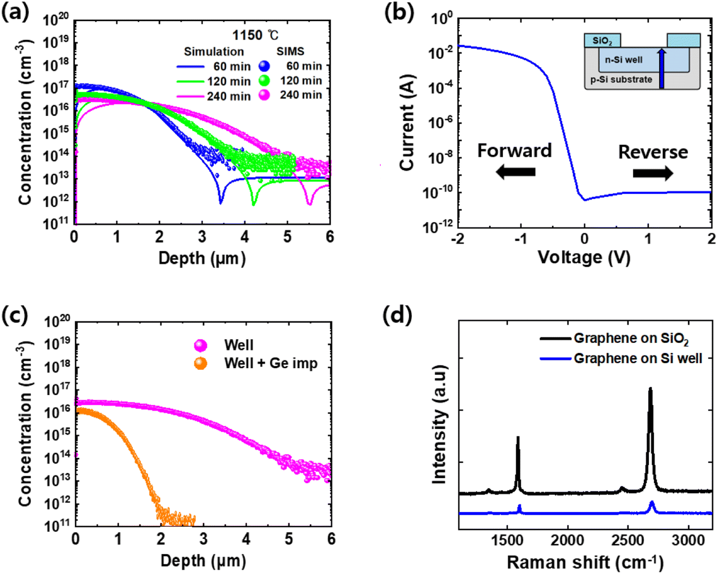 | ||
| Fig. 2 (a) Dopant profiles of phosphorus in the p-Si substrate (solid line: simulated data, scattered dot: real SIMS measurement data). Each dopant profile had different annealing time for activation. (b) PN junction leakage current measurement (p-Si substrate/n-Si well junction). (c) SIMS profiles after Ge ion implantation (d) Raman spectrum of transferred monolayer graphene on SiO2, Si well. | ||
The graphene sheet used in this study was grown on copper foil using a thermal chemical vapor deposition (TCVD) method, and the graphene sheet was transferred to the patterned SiO2/Si substrate using the polymethyl methacrylate (PMMA) mediated wet transfer method.30 In this method, the PMMA layer protected and held the graphene sheet during the transfer process. Raman analysis (Fig. 2(d)) confirmed the quality of the transferred graphene film, with the G peak at 1580 cm−1 and the 2D peak at 2680 cm−1 detected. The defect peak at 1350 cm−1 was not observed, indicating that the quality of graphene transferred onto the active region was well maintained during the transfer process.31 Graphene transfer to the sidewall of oxide trench can cause physical defects (SEM images shown in Fig. S1 in ESI†), depending on the transfer process and the quality of graphene. Following the graphene transfer, a 30 nm thick Au hard mask layer was deposited using an electron-beam evaporator (E-beam) to minimize organic residue during subsequent photolithography. The graphene outside the active and source contact region was etched off with an O2 plasma etch process. After graphene channel patterning, another contact window was formed within the well region to create a drain contact. SiO2 in the drain contact area was etched using BOE, and 100 nm of Au was deposited using an E-beam evaporation process. This Au layer served to form both source and drain electrodes (Fig. 1(c)) through an additional photolithography and Au etching process. Finally, a 30 nm layer of aluminum oxide (Al2O3), as a dielectric passivation layer, was deposited on top of the photodetector at 130 °C using an atomic layer deposition (ALD) process. Post-deposition annealing (PDA) was then carried out at 300 °C for 1 hour in a vacuum environment to eliminate water molecules at the interface between graphene and Si and densify the Al2O3 passivation layer.20
The current–voltage characteristics of the fabricated photodetectors were assessed using a semiconductor parameter analyzer (Keithley 4200). All measurements were conducted at room temperature. An 850 nm solid-state laser diode served as the near-infrared light source, with a laser pulse rise time of 47 ns. The power of the light source was quantified using a Newport Model 1917-C power meter. Detailed information about the measurement setup is provided in Fig. S2 (ESI†).
3. Results and discussion
Fig. 3(a) shows the I–V characteristics of the graphene/n-type bulk Si photodetector and graphene/n-Si well-tub/p-Si photodetectors. The current was measured under dark and illuminated conditions at 40 mW cm−2. The I–V curve shows that the graphene/Si heterostructure photodetectors behave like typical rectifying Schottky diodes and the rectification ratios at ±1 V are higher than 3 orders of magnitude for all devices. The barrier height of the graphene/Si Schottky junction can be obtained from the ideal diode equation as follows: | (1) |
 | (2) |
 | (3) |
 | ||
| Fig. 3 (a) Photoresponse of graphene/n-type bulk Si photodetector (pristine), graphene/n-Si well tub/p-Si photodetectors and photodetector with Ge ion implantation. The illumination condition was 850 nm of wavelength and 40 mW cm−2. (b) The energy band diagram of a graphene/n-Si well junction under illumination condition. (c) Photocurrent when turned on/off repeatedly over time of the device containing well-tub structure. (d) Responsivity of each device at −0.5 V. The graphene/bulk Si photodetector has the highest responsivity. (e) Photocurrent (Iph, left black axis) and responsivity (R, right blue axis) as a function of incident light power of graphene/n-type bulk Si photodetector and (f) graphene/n-Si well tub/p-Si photodetector and photodetector with Ge ion implantation. | ||
The Schottky barrier heights for the graphene/n-type bulk Si Schottky junction and the graphene/n-Si well-tub/p-type bulk Si photodetectors were 0.72 eV and 0.735, 0.738, and 0.734 eV, respectively. These values, only slightly different despite varied activation times (60, 120, and 240 min), demonstrate the excellent rectifying functions of all graphene/Si heterojunction-based devices. The photodetector subjected to 240 min of activation annealing and Ge ion implantation exhibited a barrier height of 0.728 eV. The parameters used for calculating the barrier height are listed in Table S1 (ESI†).
In Fig. 3(b), a band diagram under illumination of the graphene/n-Si well interface is presented. The Fermi level is denoted by the black dotted line, and photogenerated electrons and holes are represented by blue and red circles, respectively. The Fermi level of graphene primarily resides in the hole branch within the bias range from 1 V to −1 V (Fig. S3†). Band bending occurs at the graphene/n-Si well interface to align the Fermi levels of graphene and n-well silicon. Photogenerated holes move toward graphene, and electrons move toward silicon well following the direction of band bending. Consequently, the photocurrent flows from silicon to graphene. Fig. 3(c) displays the real-time photocurrent response of the graphene/n-Si well-tub/p-Si photodetector device under 850 nm illumination at Vd = −0.5 V. The response was measured by alternately turning the laser diode on and off at 10 s intervals. Even with variations in power and repeated measurements, the responses remained consistent without any signs of degradation. This result is similar to the previously reported 2D material/semiconductor heterojunction-based photodetectors and indicates that the device fabricated in an isolated well-tub structure can operate stably for the repetitive switching conditions.
Next, Fig. 3(d) illustrates the responsivity of each device. Responsivity is an indicator used to evaluate the performance of a photodetector and is expressed by the following equation:
 | (4) |
The steady-state photocurrent density (JL) due to reverse bias and photogenerated carriers in the depletion region can be expressed by the following equation:
 | (5) |
 | ||
| Fig. 4 (a) Cross-sectional schematic of the graphene/n-type bulk Si photodetector. (b) The energy band diagram of a graphene/n-type bulk Si photodetector under illumination conditions. (c) Scanning photocurrent microscopy image of the graphene/n-type bulk Si photodetector (left) and graphene/n-Si well-tub/p-Si photodetector (right), both presented on the same scale. The black dashed areas indicate the junction of graphene and Si (Vd = −0.5 V, λ = 850 nm). | ||
Moreover, scanning photocurrent microscopy (SPCM) was employed to compare the primary carrier generation region and the amount of photocurrent between the two devices (bulk and well tubs), as shown in Fig. 4(c). The photocurrent from each point was measured while scanning the entire device region with a laser (a pixel diameter of 4 μm). The left image depicts the photocurrent map of the bulk Si-substrate-based device, and the right image illustrates the photocurrent map of the device with an isolated well structure. In both devices, most of the photocurrent formed in the graphene/Si junction area; however, the amount of photocarrier differed by approximately two times. This is because the bulk-Si-based photodetector has an additional gain in addition to the photocarrier formed at the graphene/Si Schottky junction; but it requires more time to collect carriers from distant region. Since the isolated well structure blocks carriers from the bulk substrate and collects only the photocarriers formed near the Si surface, it is expected to have lower photocurrent generation but a fast-operating speed.
The response times of the devices were measured after analyzing the electrical properties of the graphene/Si heterojunction photodetectors. The rise time of the photodetector (τr) was extracted from the time required to reach from 10% to 90% of the signal level generated by light. Fig. 5(a) shows the rising part of the response pulse measured using a graphene/n-type bulk Si photodetector. Bulk Si-based devices can collect carriers not only from the graphene/Si junction but also from the remote part of the substrate and the neighbouring region. Assuming that they were collected laterally from the deep part of the electrode, the rise time was expected to be between 11–22.1 μs. The equations and parameters used for this calculation are listed in Table S2 (ESI†). The actual measured rise time value was 12.6 μs, consistent with the rough estimation. On the other hand, Fig. 5(b) shows the response curve of the graphene/n-Si well-tub/p-Si photodetectors. The τr in these devices had a maximum value of 115.1 ns. The large difference between these two structures was primarily due to the difference in the carrier transport time. Interestingly, the response time was not dependent on well depth, indicating that there was no significant difference in the vertical transport time. By eliminating photocarriers from outside the well structure, the response time can be improved by more than two orders of magnitude.
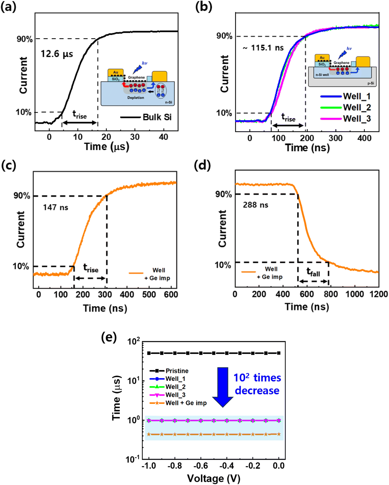 | ||
| Fig. 5 Photocurrent as a function of time for (a) the graphene/n-type bulk Si photodetector, (b) the graphene/n-Si well tub/p-Si photodetectors with different well depths and (c) and (d) the photodetector with Ge ion implantation. (e) The minimum pulse width (sum of rise time and fall time) as a function of drain voltage. The upper black data represent the rise time of the graphene/n-type bulk Si photodetector, while the lower colored data correspond to values for photodetectors containing the well-tub structure and the photodetector with Ge ion implantation. | ||
Fall time was also improved by the introduction of the well tub structure from 38 μs to 858 ns, which is primarily explained by the limited volume of the region containing photocarriers. To further improve the falling time, physical defects were intentionally introduced into the well region by implanting Ge, as shown in Fig. 5(c) and (d). After Ge implantation, τf decreased from 858 ns to 288 ns while the τr increased from 115 ns to 147 ns. Overall, the minimal pulse width that can be applied to the photodetector decreased to 435 ns from 50.6 μs, enabling ∼2 MHz operation. The performance of our device with a well tub and Ge implantation was compared with that of similar 2D/semiconductor heterojunction photodetectors reported in the literature, as shown in Table 1.
| Device structure | Wavelength (nm) | V DD (V) | Responsivity (A W−1) | Rise time (τr, μs) | Fall time (τf, μs) | Ref. |
|---|---|---|---|---|---|---|
| Graphene/Si | 850 | 0.5 | 1.25 | 12.6 | 38.0 | This work |
| Graphene/Si well-tub | 850 | 0 | 0.06 | 0.117 | 0.860 | |
| 0.5 | 0.56 | 0.115 | 0.858 | |||
| Graphene/Si well-tub + Ge-induced defect | 850 | 0 | 0.05 | 0.150 | 0.291 | |
| 0.5 | 0.29 | 0.147 | 0.288 | |||
| Graphene/crystalline Si | 850 | 0 | 0.029 | 93 | 110 | 38 |
| Graphene/Si | 632 | 5 | 104 | 3 | — | 39 |
| 1550 | 0.23 | |||||
| Graphene/Si | 890 | 0 | 0.73 | 320 | 750 | 40 |
| Graphene/Si | 1550 | 2 | 0.04 | 5 | 8 | 26 |
| Graphene nanofilms/Si | 1870 | 1 | 0.0004 | 0.317 | 0.261 | 41 |
After confirming the performance of the devices with different structures, their photocharacteristics were analyzed as a function of the drain bias. Fig. 5(e) shows the minimum pulse width (τr + τf) of photodetectors measured as a function of drain bias ranging from 0 V to −1.0 V. The distribution of the data was below 5% at a bias above −0.1 V. The operating speed at zero bias was improved by 50 times, indicating that very low-power operation was feasible with this device. Furthermore, the responsivity of this device can be further improved even at zero bias by applying various methods, such as graphene doping or gate modulation, to increase the height of the Schottky barrier formed at the graphene/Si junction.24,36,37
4. Conclusions
There are several methods to improve the speed of the photodetector further, including using semiconductor materials with excellent carrier mobility such as GaAs or InP, scaling the size of unit device, and modifying the structure of the device to minimize the lateral transport time. In this study, a high-speed graphene/Si heterostructure photodetector was developed by incorporating a well-structured design with Ge recombination centers. The rise time was reduced to 115 ns, achieving a responsivity of 0.56 A W−1 in the near-infrared region. This performance represents an improvement of over two orders of magnitude compared to previously reported graphene/bulk Si heterojunction devices. Furthermore, the fall time decreased to 288 ns from 858 ns with the introduction of Ge-induced defect recombination centers into the well, albeit resulting in a reduced responsivity of 0.29 A W−1. Overall, the device demonstrated high-speed operation surpassing 2 MHz at 0.5 V. These findings suggest that a graphene/Si photodetector featuring an isolated well-tubed structure holds significant promise for future high-performance optoelectronics characterized by high speed, simplified processing, and low power consumption.Conflicts of interest
There are no conflicts to declare.Acknowledgements
This research was supported by the Core Technology Development Project for National Semiconductor Research Laboratory (No. RS-2023-00260813) and Nano Materials Technology Development Program (2022M3H4A1A04096496) of the National Research Foundation of Korea (NRF), funded by the Ministry of Science and Technology Communication, Korea.Notes and references
- P. Bai, X. Li, N. Yang, W. Chu, X. Bai, S. Huang, Y. Zhang, W. Shen, Z. Fu, D. Shao, Z. Tan, H. Li, J. Cao, L. Li, E. H. Linfield, Y. Xie and Z. Zhao, Sci. Adv., 2022, 8, eabn2031 CrossRef CAS PubMed.
- M. Parakh, R. Pokharel, K. Dawkins, S. Devkota, J. Li and S. Iyer, Nanoscale, 2022, 4, 3919–3927 RSC.
- X. Li, J. Zhang, C. Yue, X. Tang, Z. Gao, Y. Jiang, C. Du, Z. Deng, H. Jia, W. Wang and H. Chen, Sci. Rep., 2022, 12, 7681 CrossRef CAS PubMed.
- J. Zhang, H. Cao, W. Bai, D. Zhao, Y. Chen, X. Wang, J. Yang, Y. Zhang, R. Qi, R. Huang, X. Tang, J. Wang and J. Chu, J. Mater. Chem. A, 2022, 10, 20837–20846 RSC.
- A. Rogalski, In HgCdTe Photodetectors: Mid-infrared Optoelectronics, Woodhead Publishing, Sawston, 2020 Search PubMed.
- I. Sharama, T. Srivastava, R. Kaushik and A. Goyal, International Conference on Signal Processing and Communication (ICSC), India, 2019, pp. 99–102 Search PubMed.
- Z. Azimi, A. Gopakumar, A. S. Ameruddin, L. Li, T. Truong, H. T. Nguyen, H. H. Tan, C. Jagadish and J. Wong-Leung, Nano Res., 2021, 15, 3695–3703 CrossRef.
- J. Miao and C. Wang, Nano Res., 2021, 14, 1878–1888 CrossRef.
- A. Bablich, D. S. Schneider, P. Kienitz, S. Kataria, S. Wagner, C. Yim, N. McEvoy, O. Engstrom, J. Muller, Y. Sakalli, B. Butz, G. S. Duesberg, P. H. Bolivar and M. C. Lemme, ACS Photonics, 2019, 6, 1372–1378 CrossRef CAS.
- O. Ozdemir, I. Ramiro, S. Gupta and G. Konstantatos, ACS Photonics, 2019, 6, 2381–2386 CrossRef CAS.
- Y. Xu, Y. Ma, Y. Yu, S. Chen, Y. Chang, X. Chen and G. Xu, Nanotechnology, 2020, 32, 075201 CrossRef PubMed.
- C. Liu, J. Guo, L. Yu, J. Li, M. Zhang, H. Li, Y. Shi and D. Dai, Light: Sci. Appl., 2021, 10, 123 CrossRef CAS PubMed.
- K. Xu, W. Zhou and Z. Ning, Small, 2020, 16, 2003397 CrossRef CAS PubMed.
- C. Livache, B. Martinez, N. Goubet, C. Greboval, J. Qu, A. Chu, S. Royer, S. Ithurria, M. G. Silly, B. Dubertret and E. Lhuillier, Nat. Commun., 2019, 10, 2125 CrossRef PubMed.
- J. Zha, M. Luo, M. Ye, T. Ahmed, X. Yu, D.-H. Lien, Q. He, D. Lei, J. C. Ho, J. Bullock, K. B. Crozier and C. Tan, Adv. Funct. Mater., 2022, 32, 2111970 CrossRef CAS.
- M. Ye, J. Zha, C. Tan and K. B. Crozier, Appl. Phys. Rev., 2021, 8, 031303 CAS.
- Z. Chen, X. Li, J. Wang, L. Tao, M. Long, S.-J. Liang, L. K. Ang, C. Shu, H. K. Tsang and J.-B. Xu, ACS Nano, 2017, 11, 430–437 CrossRef CAS PubMed.
- R. R. Nair, P. Blake, A. N. Grigorenko, K. S. Novoselov, T. J. Booth, T. Stauber, N. M. R. Peres and A. K. Geim, Science, 2008, 320, 1308 CrossRef CAS PubMed.
- M. Kole and T. K. Dey, J. Appl. Phys., 2013, 113, 084307 CrossRef.
- C. G. Kang, S. K. Lee, S. Choe, Y. G. Lee, C.-L. Lee and B. H. Lee, Opt. Express, 2013, 21, 23391–23400 CrossRef CAS PubMed.
- N. Youngblood, C. Chen, S. J. Koester and M. Li, Nat. Photonics, 2015, 9, 247–252 CrossRef CAS.
- S. Lin, Y. Lu, J. Xu, S. Feng and J. Li, Nano Energy, 2017, 40, 122–148 CrossRef CAS.
- S. W. Howell, I. Ruiz, P. S. Davids, R. K. Harrison, S. W. Smith, M. D. Goldflam, J. B. Martin, N. J. Martinez and T. E. Beechem, Sci. Rep., 2017, 7, 14651 CrossRef PubMed.
- K. E. Chang, T. J. Yoo, C. Kim, Y. J. Kim, S. K. Lee, S.-Y. Kim, S. Heo, M. G. Kwon and B. H. Lee, Small, 2018, 14, 1801182 CrossRef PubMed.
- A. D. Bartolomeo, Phys. Rep., 2019, 606, 1–58 CrossRef.
- C. Wang, Y. Dong, Z. Lu, S. Chen, K. Xu, Y. Ma, G. Xu, X. Zhao and Y. Yu, Sens. Actuators, A, 2019, 291, 87–92 CrossRef CAS.
- M. Scagliotti, M. Salvato, M. D. Crescenzi, N. Mishra, F. Fabbri, V. Miseikis, C. Coletti, D. Catone, L. D. Mario, M. Boscardin and P. Castrucci, Nanotechnology, 2021, 32, 155504 CrossRef CAS PubMed.
- F. Cristiano, Ion Implantation-Induced Extended Defects: Structural Investigations and Impact on Ultra-Shallow Junction Properties, Université Paul Sabatier-Toulouse III, France, 2013 Search PubMed.
- D. Klinger, J. Auleytner, D. Zymierska, B. Kozankiewicz, A. Barcz, L. Nowicki and A. Stonert, Eur. Phys. J.: Appl. Phys., 2004, 27, 149–153 CrossRef CAS.
- G. B. Barin, Y. Song, I. F. Gimenez, A. G. S. Filho, L. S. Barreto and J. Kong, Carbon, 2015, 84, 82–90 CrossRef.
- A. C. Ferrari and D. M. Basko, Nat. Nanotechnol., 2013, 8, 235–246 CrossRef CAS PubMed.
- D. K. Schroder, Semiconductor material and device characterization, John Wiley & Sons, Inc., New York, 2005 Search PubMed.
- E. H. Rhoderick and R. H. Williams, Metal-Semiconductor Contacts, Clarendon Press, Oxford, 1988 Search PubMed.
- G. Konstantatos, M. Badioli, L. Gaudreau, J. Osmond, M. Bernechea, F. Pelayo, G. Arquer, F. Gatti and F. H. L. Koppens, Nat. Nanotechnol., 2012, 7, 363–368 CrossRef CAS PubMed.
- K. E. Chang, C. Kim, T. J. Yoo, M. G. Kwon, S. Heo, S.-Y. Kim, Y. Hyun, J. I. Yoo, H. C. Ko and B. H. Lee, Adv. Electron. Mater., 2019, 5, 1800957 CrossRef.
- T. J. Yoo, S.-Y. Kim, M. G. Kwon, C. Kim, K. E. Chang, H. J. Hwang and B. H. Lee, Laser Photonics Rev., 2021, 15, 2000557 CrossRef CAS.
- G. Luongo, A. Grillo, F. Urban, F. Giubileo and A. D. Bartolomeo, Mater. Today, 2020, 20, 82–86 CrossRef CAS.
- P. Lv, X. Zhang, X. Zhang, W. Deng and J. Jie, IEEE Electron Device Lett., 2013, 34, 1337–1339 CAS.
- Z. Chen, Z. Cheng, J. Wang, X. Wan, C. Shu, H. K. Tsang, H. P. Ho and J.-B. Xu, Adv. Opt. Mater., 2015, 3, 1207–1214 CrossRef CAS.
- X. Li, M. Zhu, M. Du, Z. Lv, L. Zhang, Y. Li, Y. Yang, T. Yang, X. Li, K. Wang, H. Zhu and Y. Fang, Small, 2016, 12, 595–601 CrossRef CAS PubMed.
- L. Liu, X. Cao, X. Liu, Z. Zhang, X. Wang and Y. Xu, IEEE Trans. Nanotechnol., 2022, 21, 307–310 CAS.
Footnote |
| † Electronic supplementary information (ESI) available. See DOI: https://doi.org/10.1039/d4na00286e |
| This journal is © The Royal Society of Chemistry 2024 |