
 Open Access Article
 This Open Access Article is licensed under a
 Creative Commons Attribution 3.0 Unported Licence
Enhanced photocatalytic water splitting with two-dimensional van der Waals heterostructures of BAs/WTeSe†
BiBi
Hanifan
a,
Abdul
Jalil
 a,
Syed Zafar
Ilyas
a,
Azeem
Ghulam Nabi
*bc and
Devis
Di Tommaso
*cd
a,
Syed Zafar
Ilyas
a,
Azeem
Ghulam Nabi
*bc and
Devis
Di Tommaso
*cd
aDepartment of Physics, Allama Iqbal Open University, Islamabad, 44000, Pakistan
bDepartment of Physics, Hafiz Hayat Campus, University of Gujrat, Gujrat, 50700, Pakistan. E-mail: azeem.nabi@uog.edu.pk; imagnabi@gmail.com
cDepartment of Chemistry, School of Physical and Chemical Sciences, Mile End Road, London, Queen Mary University of, London, E1 4NS, UK. E-mail: d.ditommaso@qmul.ac.uk
dDigital Environment Research Institute, Queen Mary University of London, Empire House, 67-75 New Road, London, E1 1HH, UK
First published on 4th April 2024
Abstract
The photocatalytic efficiency of monolayer materials can be significantly enhanced by constructing two-dimensional van der Waals heterostructures. This study presents first principles calculations based on density functional theory to investigate the electronic properties and photocatalytic mechanism of van der Waals heterostructures of boron arsenide (BAs) with the Janus MXY (M = W; X/Y = Se, Te) monolayers, with and without Se vacancies. Results from binding energies, phonon spectra, and ab initio molecular dynamics simulations indicate that the heterostructures are thermodynamically stable. The deformation potential theory was then used to investigate carrier mobility μ in 2D materials. All the heterostructures exhibit direct bandgaps with valence band maxima and conduction band minima suitable for water splitting. Additionally, these heterostructures possess high optical absorption coefficients in the visible and ultraviolet regions. In particular, our calculations predict BAs/WTeSe, with and without Se vacancies, as promising candidates for photocatalytic water splitting applications.
Introduction
The finite nature of fossil fuels, coupled with their detrimental environmental impact and contribution to climate change, has exacerbated environmental contamination and energy crises, posing significant challenges to humanity.1 Finding a sustainable energy source to replace finite fossil fuels is crucial. Hydrogen generated by photocatalytic water splitting is regarded as a sustainable, clean, and renewable energy source for the future.2–4 However, finding the right photocatalyst is essential to producing hydrogen energy from water splitting. The large band gap and improper alignment of band edge position are the main hurdles for a suitable photocatalyst for water splitting.5–7Graphene, a two-dimensional (2D) material, has been extensively studied for its applications in electronic and optoelectronic devices, even though it lacks a tunable band gap.8 Consequently, new types of 2D materials have been explored in recent years, including phosphorene,9 transition-metal dichalcogenides (TMDs),10 and MXenes.11 Compared with the bulk counterparts, TMDs have enhanced charge transfer and separation capabilities due to their large specific surface area and are thus promising materials for application in optoelectronic devices, transistors and sensors.10 Among TMDs, WX2 (X = S, Se, Te)12 monolayers have been widely studied theoretically and experimentally. WS2, WSe2 and MoSe2 monolayers are excellent high-temperature thermoelectric materials.
A recent breakthrough in the realm of 2D TMDs has led to the synthesis of Janus MXY (M = W, Mo; X/Y = Se, S, Te) monolayers through vulcanization or selenization experiments employing the CVD method.13 Unlike their mirror-symmetric counterparts MoS2 and MoSe2, the MoSSe monolayer is fabricated via selective selenization of the top atomic layer in a single-layer MoS2 structure. The electronegativity difference between sulfur and selenium atoms induces interlayer polarization in Janus materials, enabling coupling with the inherent interlayer built-in polarization field. This unique property introduces an additional degree of freedom for modulating their physicochemical properties, garnering significant attention due to their novel features and promising applications. Moreover, Janus-WSeTe or Janus-WTeSe monolayers are direct band gap semiconductors with moderate band gaps.14 Unfortunately, not all 2D materials are suitable for water splitting because their band gap values may be too large and the band edge alignment may be located far from the redox potentials.
To address these limitations, the synthesis of van der Waals heterostructures (vdWHs) have been proposed as a promising strategy to engineer suitable band edge positions for water splitting.15–21 Arsenide semiconductors, such as boron arsenide (BAs),22 aluminum arsenide (AlAs),23 gallium arsenide (GaAs),5,24 and indium arsenide (InAs),25 have emerged as promising candidates for vdWHs due to their favorable band alignments and light absorption properties. These materials belong to groups III–V of compound semiconductor materials26–29 and play a vital role in making microwave devices,30,31 Hall devices,32 high-speed digital circuits,33 lasers,34,35 magneto-resistive devices,7,35 and detectors.36 Hexagonal BAs monolayer with a flat honeycomb structure like graphene has drawn attention as a potential photocatalyst for water splitting.37 BAs has a direct band gap, high carrier mobility, and high in-plane mechanical stability and it is the only semiconductor material with an ultrahigh thermal conductivity of 2000 W m−1 K−1 at room temperature. Consequently, BAs monolayer has been recently combined with many other 2D materials such as the vdWHs BAs/MoTe2,6 BAs/MoSe2,38 BAs/SnC,39 and BAs/GaN.40
This paper investigates using density functional theory (DFT) calculations the photocatalytic properties of BAs/Janus WSeTe and BAs/Janus WTeSe vdWHs as possible direct Z-scheme photocatalysts. Stacking-based approaches have been employed to investigate the electrical, optical and photocatalytic properties of all the suggested systems. We found that many configurations of these heterostructures are suitable for tuning optoelectronic characteristics for photocatalysis applications, either type-II or Z-scheme. Although the built-in electric field under various stacking configurations favours the development of Z-scheme charge transfer, not all of them belong to Z-scheme according to work function and charge density difference. In reality, the classification of the system as type-II or Z-scheme depends on the competition between charge separation and interlayer e−h+ recombination. Furthermore, by introducing Te vacancy defects, the charge transfer channel in Janus BAs/WTeSe heterostructures can be successfully flipped from type-II to Z-scheme, which may effectively regulate this competitive relationship. Remarkably, Te vacancy defects can increase the time interval between electron (hole) transmission. Our findings show that the BAs/Janus WTeSe vdWHs have strong photocatalytic activity and that the proposed class-II configuration is ideally suited for highly efficient water splitting.
Methods
All DFT calculations were conducted using the Vienna ab initio simulation package (VASP)41 and the projector augmented wave (PAW) potential method.42 Geometry optimization and ab initio molecular dynamics (AIMD) were performed using the Perdew–Burke–Ernzerhof (PBE) generalized gradient approximation (GGA)43 in conjunction with Grimme's D3 (PBE-D3) method to accurately describe the van der Waals interactions between BAs and Janus-WSeTe.44 As generally PBE underestimates the band gap of semiconductors, single point calculations were conducted using the hybrid HSE06 (Heyd–Scuseria–Ernzerhof) functional. HSE06 was also used to compute the optical properties of the abovementioned heterostructures and monolayers.45 Convergence tolerances were set to 10−6 eV for the energy and 0.01 eV Å−1 for the force. To ensure calculation accuracy, the k-point (Monkhorst–Pack) grid was set to (15 × 15 × 1) together with a cutoff energy of 520 eV for ensuring calculation accuracy. The vacuum space was set to 25 Å to minimise the interaction between adjacent layers. AIMD simulations were performed with a (4 × 4 × 1) supercell at the Γ point for 6 ps using a 1 fs timestep in the NVT ensemble (constant volume and temperature) at T = 300 K and T = 500 K.46 The phonon dispersion curve calculations were also performed with a 4 × 4 × 1 supercell in the framework of frozen-phonon approximation.47Results and discussion
Structural properties
To construct the initial models of 2D BAs–Janus WSeTe vdWHs, the structures of the isolated hexagonal BAs and WSeTe monolayers were optimized first. The optimized structural parameters of BAs and WSeTe are summarized in Table 1. The lattice constants of BAs are a = b = 3.39 Å, and the B–As bond length is 1.96 Å. In the literature, the lattice constants of monolayer BAs obtained by DFT calculations have been reported as a = b = 3.39 Å and the bond length between B and As atoms is 1.95 Å.48 The Janus WSeTe monolayer has lattice constants of a = b = 3.45 Å, with bond lengths of 2.55 Å and 2.71 Å between W–Se and W–Te atoms, respectively. Sun et al. had investigated this structure and found the lattice parameters of the hexagonal WSeTe to be a = b = 3.405 Å.49,50 The BAs with Janus-WSeTe and BAs with Janus-WTeSe monolayers were used to construct 12 vdW heterostructure configurations. They were categorized into two classes: (i) BAs/Janus WSeTe vdWHs, where the BAs monolayer is close to the Se atom of the Janus-WSeTe monolayer; (ii) BAs/Janus WTeSe vdWHs, where the BAs layer is close to the Te atoms of the Janus WTeSe monolayer. For these two classes of heterostructures, six different stacking configurations are possible, as shown in Fig. 1.| System | a (Å) | d (Å) | E g (eV) | ΔE | ||
|---|---|---|---|---|---|---|
| Method | PBE | PBE-D3 | HSE | PBE | ||
| BAs | ||||||
| 3.390 | — | — | 1.37 | 0.75 | — | |
| WSeTe | ||||||
| 3.451 | — | — | 1.80 | 1.35 | — | |
| BAs/Janus WSeTe | ||||||
| Stacking-A | 3.392 | 4.208 | 3.71 | 1.29 | 0.712 | −0.198 |
| Stacking-B | 3.392 | 4.214 | 3.52 | 1.43 | 0.796 | −0.225 |
| Stacking-C | 3.391 | 4.214 | 3.61 | 1.30 | 0.745 | −0.208 |
| Stacking-D | 3.392 | 4.216 | 3.44 | 1.18 | 0.682 | −0.252 |
| Stacking-E | 3.390 | 4.208 | 3.78 | 1.28 | 0.694 | −0.189 |
| Stacking-F | 3.391 | 4.172 | 3.39 | 1.28 | 0.709 | −0.251 |
| BAs/Janus WTeSe | ||||||
| Stacking-A | 3.390 | 4.470 | 3.99 | 0.86 | 0.374 | −0.195 |
| Stacking-B | 3.390 | 4.259 | 3.78 | 0.89 | 0.382 | −0.223 |
| Stacking-C | 3.391 | 4.448 | 3.85 | 0.82 | 0.309 | −0.203 |
| Stacking-D | 3.391 | 4.128 | 3.61 | 0.66 | 0.192 | −0.254 |
| Stacking-E | 3.391 | 4.462 | 4.03 | 0.92 | 0.466 | −0.186 |
| Stacking-F | 3.389 | 4.117 | 3.56 | 0.93 | 0.530 | −0.264 |
| BAs/Janus WSeTe (Se vacancy) | ||||||
| 3.375 | — | 3.51 | 1.33 | 0.72 | — | |
| BAs/Janus WTeSe (Te vacancy) | ||||||
| 3.381 | — | 3.61 | 0.59 | 0.31 | — | |
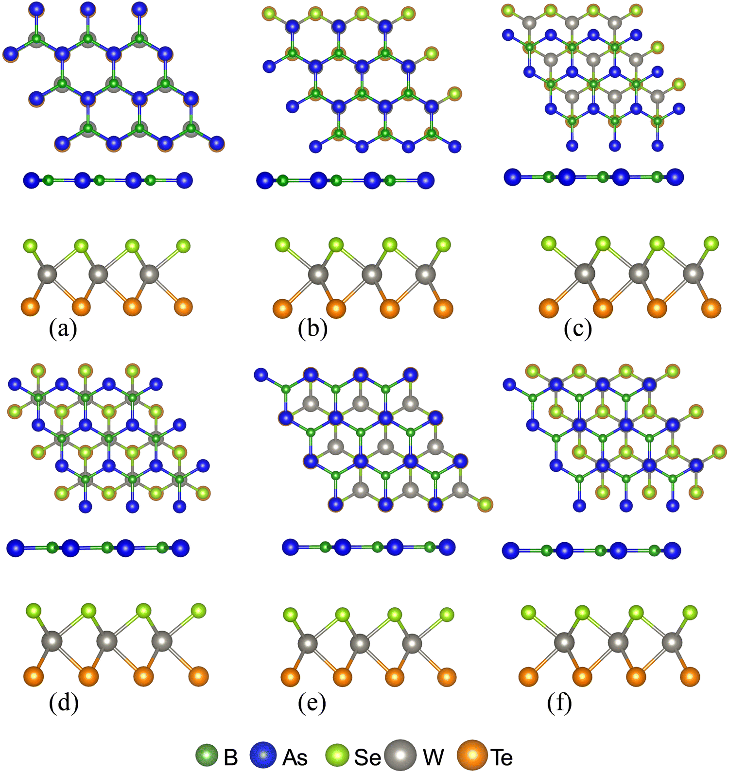 | ||
| Fig. 1 Top and side views of different configurations of vdWHs obtained from the stacking of BAs and Janus-WSeTe: (a) stacking-A – the B and As atoms sit on the top of W and Se atoms, respectively; (b) stacking-B – the B and As atoms sit on the top of Se and W atoms, respectively; (c) stacking-C – the As atom is on the hollow site of the hexagonal site, and the B atom occupies the top of the Se atom; (d) stacking-D – the As atom is on the hollow site of the hexagonal site, and the B atom occupies the top of the W atom; (e) stacking-E – the As atom sits on the top of the Se atom, while the B atom is on the center of the hexagonal site; (f) stacking-F – the As atom sits on the top of the W atom, while the B atom is on the center of the hexagonal site, BAs/Janus WSeTe vdW heterostructure. The BAs/Janus WTeSe vdWHs are formed by swapping the positions of Se and Te atoms in the six configurations (a)–(f). The color scheme for each atom is given at the bottom. | ||
The computed values of lattice parameters and interlayer distances of the optimized BAs/WSeTe vdWHs are listed in Table 1. Their formation energies (ΔE) were calculated according to the following equation:
| ΔE = Eheter − Elayer1 − Elayer2 | (1) |
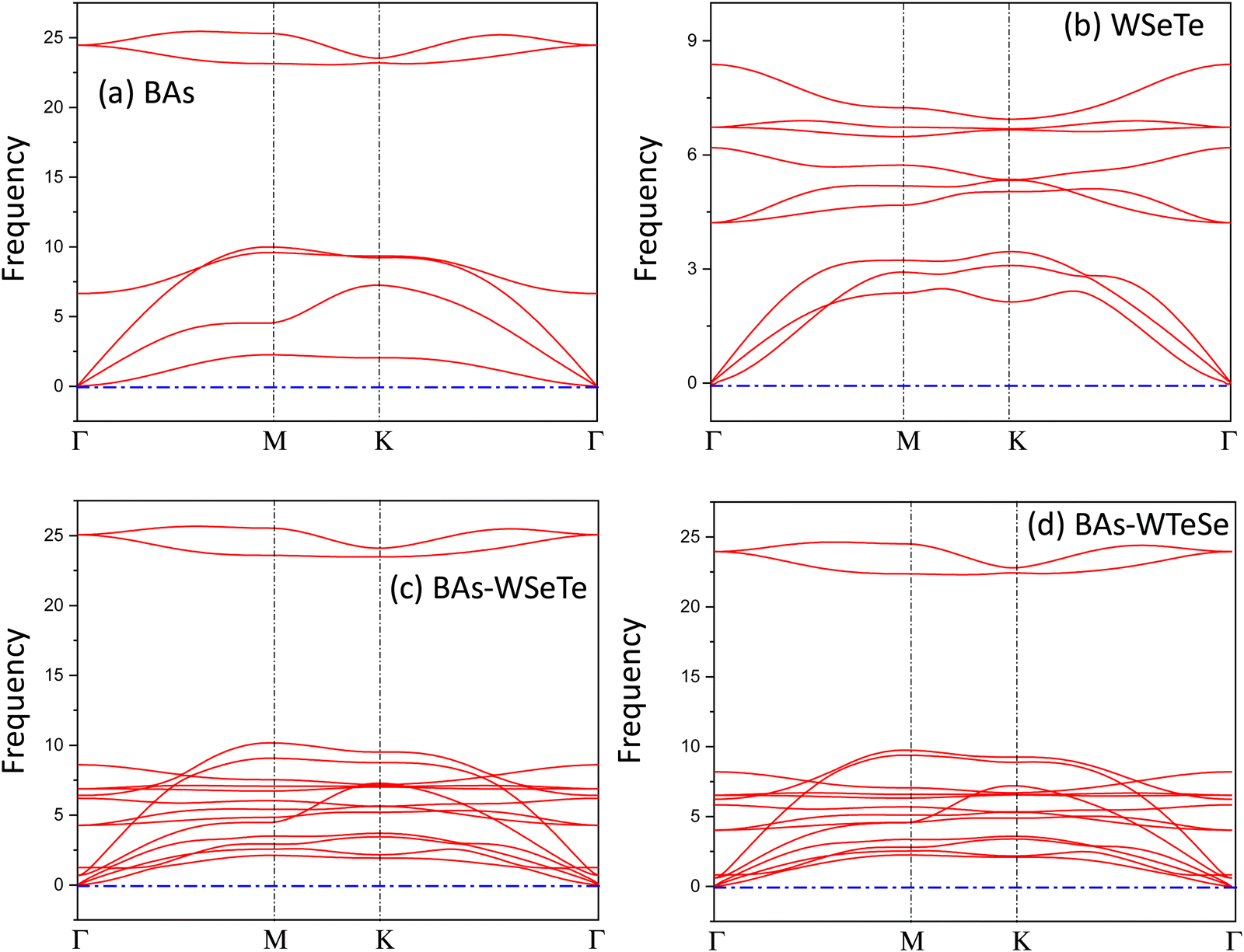 | ||
| Fig. 2 The phonon spectra of the (a) BAs, (b) WSeTe, (c) BAs–WSeTe and (d) BAs–WTeSe heterostructures. | ||
The stability of the heterostructures was investigated using AIMD simulations. For each system, simulations were conducted at T = 300 K and 500 K. Fig. S2 (ESI†) confirms that the temperatures remained stable around the target values for BAs, WSeTe, BAs–WSeTe, and BAs–WTeSe. Representative configurations from the AIMD trajectories (Fig. S3–S6, ESI†) further illustrate the thermodynamic stability of these heterostructures at both temperatures. Notably, simulations without dispersion correction showed increased interlayer spacing between BAs and WSeTe (or BAs and WTeSe) monolayers, ultimately leading to separation. This highlights the crucial role of dispersion interactions for accurately modeling such systems when using DFT methods.
The computed lattice parameters of the monolayers WSeTe and BAs are 3.45 Å and 3.39 Å, and of the heterostructures H-I, H-II, H-III and H-IV are 3.39 Å, 3.38 Å, 3.38 Å and 3.37 Å, respectively. Due to the higher value of lattice mismatch, many defects are invariably created at the interface when two single-crystalline materials are formed or fused together. For BAs and Janus-WSeTe, the lattice mismatch is only 3.3%, which is small when compared to other heterostructures.51,52 Finally, in Table 1 the inclusion of dispersion correction in the PBE functional has a significant influence on the stability of heterostructures.53 The most stable heterostructures H-I (stacking-D) and H-II (stacking-F) have lower interlayer spacing, d = 3.44 Å and d = 3.56 Å, respectively.
Electronic properties
The band structure provides insights into the electronic properties of a material. The electronic properties of the BAs and Janus WSeTe monolayers are first discussed before considering those of the BAs/Janus WSeTe heterostructure. The band structures of Janus WSeTe and BAs, computed at the PBE and HSE06 levels of theory, are presented in Fig. 3. The band gap values for the Janus WSeTe and BAs monolayers calculated using the HSE06 hybrid functional are 1.37 and 1.8 eV, respectively. Both Janus-WSeTe and BAs are direct band gap semiconductors and their conduction band minimum (CBM) and valence band maximum (VBM) reside at the same high-symmetry k-point in the Brillouin zone. Importantly, these monolayers retain their direct band gap character even after forming heterostructures.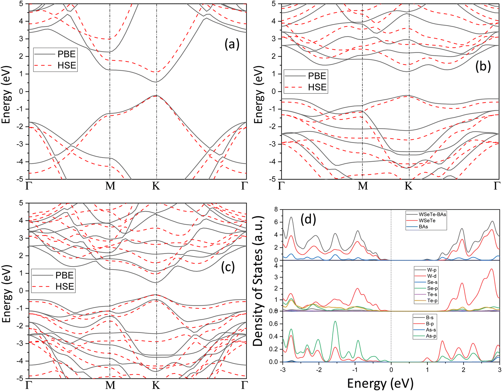 | ||
| Fig. 3 The band structures of (a) BAs, (b) Janus WTeSe, and (c) H-I heterostructure computed using the PBE (black solid lines) and HSE06 (red dashed lines) functionals. (d) Density of states of the H-I heterostructure. | ||
To investigate the electronic properties of H-I, H-II and H-III heterostructures in more detail, the total density of states (TDOS) and partial density of states (PDOS) were calculated. The CBM and VBM of the WTeSe monolayer are formed by the Te 5p, Se 4p and W 4d orbitals, respectively.50 Furthermore, the VBM of the BAs monolayer is primarily composed of As 4p orbitals, while the CBM is dominated by B 2p orbitals. These results are consistent with previous studies.22 This distinct electronic structure of BAs allows for the formation of unique band alignments at the interface when combined with other materials. Notably, both type-II and Z-scheme configurations can be achieved, depending on the specific partner material. These band alignments create favorable conditions for efficient separation of photogenerated electron–hole pairs, making BAs-based heterostructures promising candidates for photocatalytic water splitting applications. Fig. 4 shows the projected band structures of H-I and H-II. In both heterostructures, the VBM is localized on WSeTe or WTeSe (represented by blue color), while the conduction band minimum (CBM) is localized on BAs (represented by red color). H-II exhibits a smaller band gap (0.93 eV) compared to H-I (1.19 eV). The presence of Se vacancies in H-II further reduces the band gap to 0.59 eV, as shown in Fig. S7 of the ESI.†
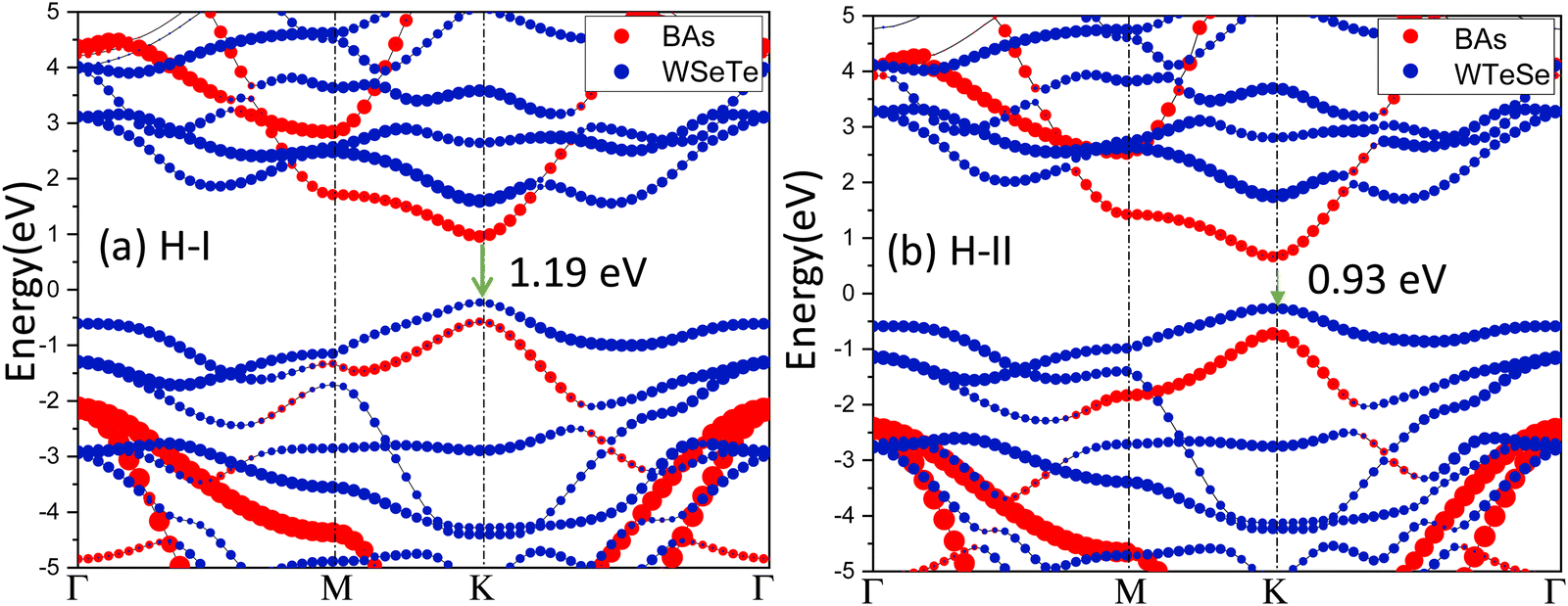 | ||
| Fig. 4 Projected band structures of the (a) H-I and (b) H-II heterostructures. | ||
Carrier mobilities
Within the framework of effective mass approximation (EMA), deformation potential (DP) theory has been a widely used approach to investigate carrier mobility (μ) in 2D materials. The carrier mobility is defined as6,54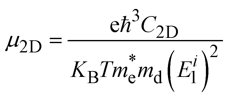 | (2) |
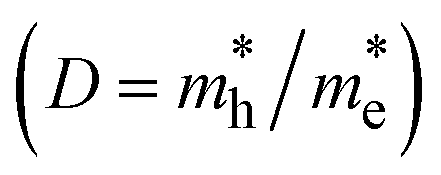
The terms in the above equation are as follows: md, the average effective mass, which is defined as 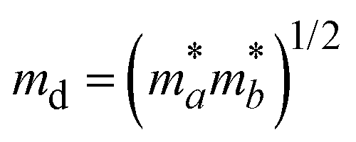 (ma and mb are the mobility of electrons or holes in the armchair (x) and zigzag (y) directions);
 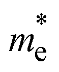 , the carrier effective mass; T, the temperature; Ei1, the DP constant, which describes the shift of the top of the valence band for holes and the bottom of the conduction band for electrons induced by the strain in the range of ±1.5% (Ei1 = ΔEi/(Δl/l0); see Fig. S8 in the ESI† for details); and C2D, the elastic modulus of a and b, uniformly deformed crystals for emulating the lattice distortion activated by the strain. For the 2D structure, the in-plane stiffness can be determined by C2D = [∂2E/∂δ2]/S0, where E is the total energy of the supercell, δ is the applied uniaxial strain, and S0 is the area of the equilibrium supercell. The details of the calculation of C2D are given in Fig. S9 of the ESI.† The large difference between the electron and hole carrier mobilities will suppress the probability of recombination of photoinduced carriers and further improve the separation of electron–hole pairs.
Photocatalytic water splitting
The design of direct Z-scheme photocatalysts either experimentally or theoretically remains a challenge.55,56 DFT calculations can be used to identify the type of the heterostructure, particularly whether it follows a direct Z-scheme or type-II configuration.57 The charge density difference (Δρ), the built-in electric field, the electron–hole recombination, the effective mass, charge carrier mobilities, and the interlayer band gaps are important parameters to understand the mechanism. The Δρ at the interface was computed according to the following equation:| Δρ = ρBAs/WSeTe − ρBAs − ρWSeTe | (3) |
| Φ = Evac − EF | (4) |
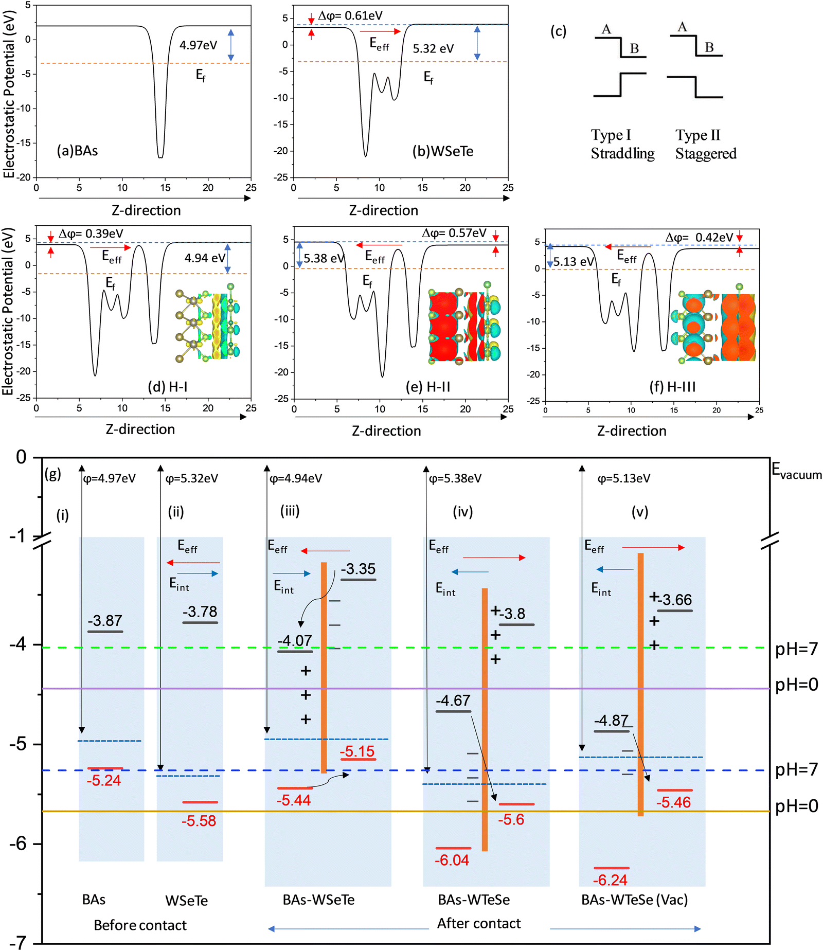 | ||
| Fig. 5 Electrostatic potential of (a) BAs; (b) WSeTe; (d) H-I; (e) H-II; and (f) H-III. (c) Mechanisms of type-I and type-II heterostructures. (g) Schematic diagram of the Z-scheme mechanism for photocatalysis (VBM in red and CBM in black). | ||
The work functions for BAs and WSeTe are Φ = 4.97 eV and Φ = 5.32 eV, respectively. Due to its higher work function, BAs exhibits a lower Fermi energy compared to WSeTe. Consequently, charge transfer occurs at the interface, with electrons moving from BAs to WSeTe. This creates an electrostatic potential (built-in electric field) pointing from BAs to WSeTe, which eventually halts further charge transfer once the Fermi energies of both materials equilibrate. This process leads to the formation of a stable heterostructure (H-I, H-II, H-III, and H-IV). Since our focus is on Z-scheme heterostructures for water splitting, WTeSe (H-II) and (H-III) were selected from the studied configurations. These configurations possess suitable band edge positions for efficient charge separation in a Z-scheme system (as shown in Table 2). While WTeSe (H-I) and (H-IV) exhibit high carrier mobilities, their band edge positions and the direction of the built-in electric field are not ideal for water splitting (Table 2). Consequently, these latter configurations may be more suitable for applications in electronic devices like diodes or transistors.59,60 However, Janus-WSeTe and Janus-WTeSe are polar materials, possessing an intrinsic electric field. This intrinsic field points in opposite directions within H-I compared to H-II and H-III. Consequently, the intrinsic field can either offset or reinforce the built-in electric field generated at the interface, leading to a net effective electric field (Eeff) across the heterostructure. In H-I, the opposing fields partially cancel each other, resulting in a weaker net Eeff. Conversely, for H-II and H-III, the fields align, leading to a stronger net Eeff. The value of Eeff depends on electrostatic potential (Dϕ) and is given by the following expression:
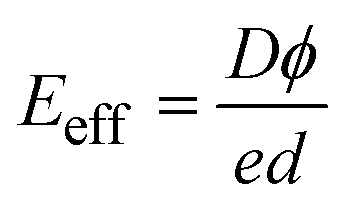 | (5) |
 . Thus, this indicates that the e−/h+ recombination will be suppressed to enhance the catalytic performance (Table S1 in the ESI†). It is important to note that WTeSe (H-II) exhibits two highly stable configurations with a small difference in the formation energies: −0.254 eV and −0.264 eV. The most stable configuration possesses a band gap value of 0.93 eV, while the second most stable configuration has a band gap of 0.66 eV (see Fig. S12 in the ESI†). Notably, the smaller band gap of the second configuration may lead to a faster rate of e−/h+ recombination at the interface of a heterostructure. The above results show that H-I is type-II, while the H-II heterostructure is a direct Z-scheme photocatalyst.
| Models |
|
|
E i 1a | E i 1b | C a /2D | C b /2D | μ a /2D | μ b /2D | |
|---|---|---|---|---|---|---|---|---|---|
| BAs | e | 0.173 | 0.256 | 2.00 | 2.02 | 156.09 | 155.69 | 23422.60 | 15475.30 |
| h | 0.172 | 0.260 | 3.01 | 3.02 | 156.09 | 155.69 | 10378.36 | 6808.04 | |
| WTeSe | e | 0.390 | 0.433 | 2.01 | 3.17 | 134.91 | 132.36 | 4543.00 | 597.77 |
| h | 0.535 | 0.675 | 5.22 | 4.91 | 134.91 | 132.36 | 337.21 | 296.29 | |
| BAs–WSeTe | e | 0.184 | 0.255 | 4.64 | 4.51 | 292.67 | 293.06 | 7468.53 | 5706.25 |
| (H-I) | h | 0.372 | 0.448 | 4.64 | 4.52 | 292.67 | 293.06 | 1961.31 | 1715.22 |
| BAs–WTeSe | e | 0.192 | 0.277 | 4.52 | 4.51 | 292.53 | 292.67 | 7071.91 | 4927.57 |
| (H-II) | h | 0.360 | 0.498 | 4.64 | 4.64 | 292.53 | 292.67 | 1953.07 | 1411.68 |
| BAs–WTeSe-v | e | 0.265 | 0.211 | 4.69 | 4.87 | 285.31 | 279.94 | 4528.44 | 5177.09 |
| (H-III) | h | 0.582 | 0.522 | 5.52 | 3.65 | 281.31 | 279.94 | 630.19 | 1598.54 |
| BAs–WSeTe-v | e | 0.271 | 0.213 | 3.11 | 5.13 | 281.91 | 276.14 | 3586.91 | 218.05 |
| (H-IV) | h | 2.488 | 1.601 | 3.66 | 4.04 | 281.91 | 276.14 | 2971.92 | 204.25 |
Water splitting requires a photocatalyst with band edges strategically positioned relative to the water redox potentials. Moreover, water splitting can only occur on the surface of heterostructures if the CBM of semiconductor-II is more positive than the reduction potential of H+/H2, and the VBM is more negative than the oxidation potential of O2/H2O. Therefore, the band alignments of H-I, H-II, and H-III were investigated, with the results presented in Fig. 5. The BAs and WTeSe monolayers are presented for comparison. The reduction potential of H+/H2 and the oxidation potential of O2/H2O at different pH values are given by6,62
 | (6) |
 | (7) |
At a pH of 7, the reduction and oxidation potentials are −4.03 eV and −5.26 eV, respectively. From Fig. 5, the CBM energies of the BAs and WSeTe monolayers and of the H-I and H-II heterostructures are higher than the reduction potential of H+/H2, while their VBM energies are lower than the oxidation potential of O2/H2O. This band alignment is favorable for photocatalytic water splitting. Fig. 6 also illustrates the photocatalytic reaction mechanism and the alteration of photoexcited carriers for H-I, H-II, and H-III heterostructures. Upon interaction with light, the heterostructure absorbs energy, causing electrons in the VBM to transition to the CBM, generating holes in the VBM and electrons in the CBM. Subsequently, the photoinjected electrons in the CBM of BAs transfer to the VBM of Janus WSeTe, as shown in Fig. 5(g)(iii). However, in this configuration, the interlayer band gap of 1.19 eV leads to a rapid electron–hole recombination process due to the small value of Δϕ (0.39 eV) and small difference between electron and hole carrier mobilities (Table 2).
 | ||
| Fig. 6 Charge density at the interfaces of pure BAs–Janus WTeSe (black) with vacancies (red) computed (a) with dipole correction and (b) without dipole correction. Vacancy defect models: (c) hexagonal and (d) orthorhombic for strain energy calculations. | ||
Swapping the Se atoms with Te atoms in the H-I heterostructure significantly reduces the interlayer band gap to 0.93 eV. This reduction in interlayer band gap slows down the e−/h+ recombination rate, facilitating charge accumulation at the VBM and CBM due to the higher value of Δϕ = 0.57 eV. This, in turn, enhances the catalytic efficiency of the heterostructure. Furthermore, introducing Te vacancies in the H-III heterostructure decreases the band gap to 0.59 eV as well as Δϕ = 0.42 eV. These vacancies generate electron and hole trapping states at the VBM and CBM, which effectively increase the mass of electrons and holes and suppress e−/h+ recombination at the interlayer, potentially influencing the catalytic performance. In Fig. 6(a), the charge density with dipole correction at the interface is presented to elaborate the Te vacancy defects in contact with BAs monolayer. As we increase the vacancy defects, the charge density flips and H-III gains a high e−/h+ recombination rate. Fig. 6 illustrates the dipole correction across the interface between BAs and the Te atom of Janus WTeSe. Without dipole corrections, the electron density difference (Δρ) appears delocalized in the middle of the interface (Fig. 6(b)). However, after considering the dipole correction term, Δρ becomes localized (Fig. 6(a)). Moreover, with Te vacancy defects, there is a flip in Δρ (Fig. 6(a)), shown in red. This flip in charge density significantly affects the built-in electric field, improving the Z-scheme heterostructure performance. Moreover, the charge carrier mobilities show that there is a large difference between electron and hole carrier mobilities that will improve the separation of e−h+ pairs (Table 2). This Z-scheme heterostructure works efficiently for water splitting due to suitable oxidation and reduction energy levels at −6.04 eV and −3.8 eV, respectively.
Further, climbing image nudged elastic band (CI-NEB) calculations were performed to investigate water splitting on BAs–WTeSe with and without Te vacancies. In both cases, the reaction from *H2O to (*H + *OH) is exothermic (ΔH = 0.06 eV and 0.16 eV), with activation energies of 0.63 eV and 0.66 eV, respectively. The presence of a Te vacancy slightly favors the water splitting reaction, as indicated by the lower activation energy (0.63 eV) compared to the pristine surface (0.66 eV). The saddle point was confirmed by frequency calculations for H-II and H-III, which showed only one imaginary frequency of 1237.6 cm−1 and 1238.0 cm−1, respectively. These imaginary frequencies correspond to the vibrational mode of the breaking H–O bond in water, confirming the reaction pathway (Fig. 7).
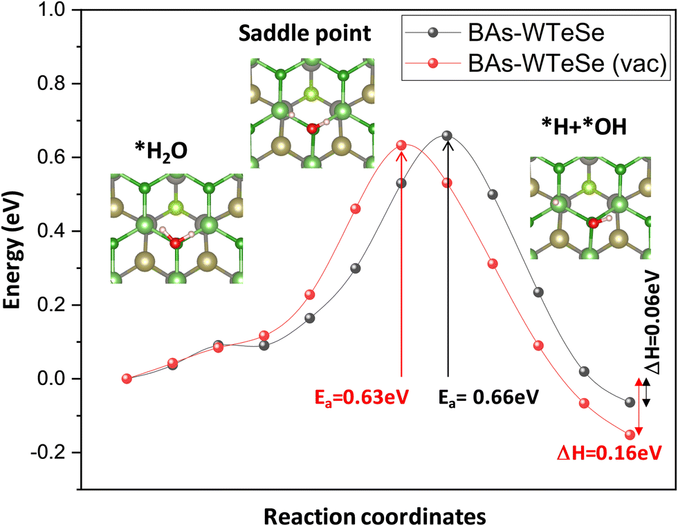 | ||
| Fig. 7 Reaction profiles for the water splitting on BAs–WTeSe without Te vacancies (black line) and BAs–WTeSe with Te vacancies (vac) (red line). | ||
Furthermore, to verify the stability of the BAs/WTeSe van der Waals heterostructures under reaction conditions, AIMD simulations of BAs–WTeSe, with and without Te vacancies, in contact with 90 water molecules were conducted. The simulations were performed in the NVT ensemble at 300 K for a total simulation time of 5 ps with a timestep of 1 fs. The structural integrity of the proposed heterostructures was maintained throughout the simulations, as evidenced in Fig. S10 (ESI†) by the well-preserved structure of the final configuration. Additionally, Fig. 11 (ESI†) demonstrates the stability of the total energy of the system over the simulation time, with no significant fluctuations observed. These results strongly suggest that the BAs/WTeSe heterostructures exhibit good stability in the presence of water molecules, making them promising candidates for water splitting applications.
Optical properties
The photocatalytic efficiency of a photocatalyst depends on its ability to capture photons in the visible region (380 to 760 nm). The light absorption coefficient is given as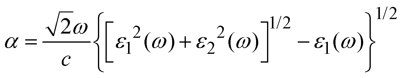 | (8) |
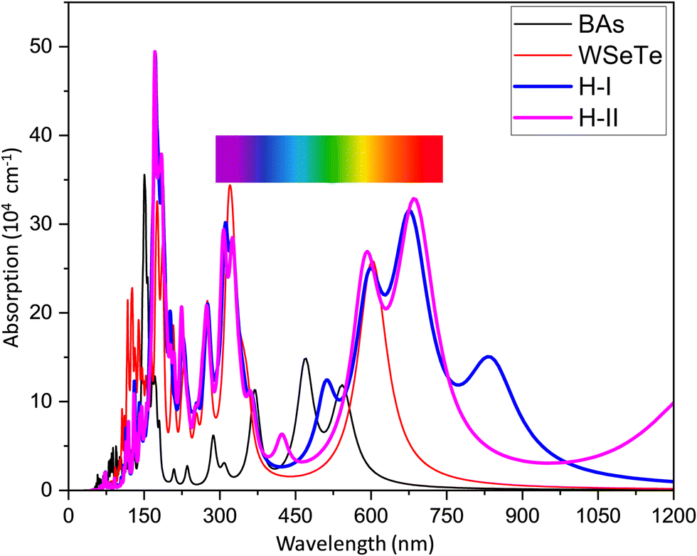 | ||
| Fig. 8 The absorption coefficient of the monolayers BAs, WSeTe, and two different heterostructures. | ||
Conclusions
In summary, DFT calculations were employed to investigate the electronic properties and photocatalytic mechanism of BAs/Janus-WSeTe and BAs/Janus-WTeSe heterostructures. The stability of these heterostructures was verified by phonon spectrum analysis and ab initio MD simulations. Our results revealed the formation of type-II and Z-scheme heterostructures with direct band gap values of 1.19 eV and 0.93 eV, respectively. Charge carrier mobilities calculated using DP theory reveal that electron–hole recombination is significantly suppressed in the Z-scheme heterostructure with Te vacancies, leading to a reduced interlayer band gap of 0.59 eV. Charge redistribution at the interface induced a built-in electric field. Upon interaction with visible light, this built-in electric field accumulated photoinjected holes in the VBM of Janus-WSeTe or Janus-WTeSe and photoinjected electrons in the CBM of BAs. Overall, the Z-scheme (BAs/Janus-WTeSe) heterostructure exhibited superior catalytic efficiency compared to the type-II (BAs/Janus-WSeTe) heterostructure, demonstrating its potential as a promising catalyst for water splitting.Author contributions
Conceptualisation of work: HBB, AJ, SZI, AGN and DDT; conducting of experiments: HBB and AGN; computations: HBB and AGN; data analyses: HBB, SZI, AGN and DDT; data dissemination and graphics: HBB, SZI, AGN, and DDT; writing of manuscript: HBB, AJ, AGN, and DDT; project support: DDT.Conflicts of interest
There are no conflicts to declare.Acknowledgements
Calculations were performed using the U.K. National Supercomputing Facility ARCHER2 (https://www.archer2.ac.uk) via our membership of the U.K.'s HEC Materials Chemistry Consortium, which is funded by the EPSRC (grants EP/L000202 and EP/R029431) and the Molecular Modelling Hub for computational resources, MMM Hub, which is partially funded by the EPSRC (EP/P020194/1). This research utilised Queen Mary's Apocrita HPC facility, supported by QMUL Research-IT (https://doi.org/10.5281/zenodo.438045). We acknowledge the assistance of the ITS Research team at Queen Mary University of London.References
- N. Raza, W. Raza, H. Gul and K. H. Kim, ZnO–ZnTe hierarchical superstructures as solar-light-activated photocatalysts for azo dye removal, Environ. Res., 2021, 194, 110499, DOI:10.1016/j.envres.2020.110499.
- R. M. Navarro Yerga, M. Consuelo Álvarez Galván, F. del Valle, J. A. Villoria de la Mano and J. L. G. Fierro, Water splitting on semiconductor catalysts under visiblelight irradiation, ChemSusChem, 2009, 2(6), 471–485, DOI:10.1002/cssc.200900018.
- S. Wang, C. Ren, H. Tian, J. Yu and M. Sun, MoS2/ZnO van der Waals heterostructure as a high-efficiency water splitting photocatalyst: A first-principles study, Phys. Chem. Chem. Phys., 2018, 20(19), 13394–13399, 10.1039/c8cp00808f.
- X. Ma, X. Wu, H. Wang and Y. Wang, A Janus MoSSe monolayer: A potential wide solar-spectrum water-splitting photocatalyst with a low carrier recombination rate, J. Mater. Chem. A, 2018, 6(5), 2295–2301, 10.1039/c7ta10015a.
- T. W. Kim, D. Kim, Y. Jo, J. Park, H. S. Kim and C. H. Shin, van der Waals Heteroepitaxy of Te Crystallites/2H-MoTe2 Atomically Thin Films on GaAs Substrates by Using Metal-Organic Chemical-Vapor Deposition, J. Korean Phys. Soc., 2020, 76(2), 167–170, DOI:10.3938/jkps.76.167.
- M. Cao, et al., DFT investigation on direct Z-scheme photocatalyst for overall water splitting: MoTe2/BAs van der Waals heterostructure, Appl. Surf. Sci., 2021, 551, 149364, DOI:10.1016/j.apsusc.2021.149364.
- A. Nabi, The electronic and the magnetic properties of Mn doped wurtzite CdS: First-principles calculations, Comput. Mater. Sci., 2016, 112, 210–218, DOI:10.1016/j.commatsci.2015.10.039.
- D. H. Lim, J. H. Jo, D. Y. Shin, J. Wilcox, H. C. Ham and S. W. Nam, Carbon dioxide conversion into hydrocarbon fuels on defective graphene-supported Cu nanoparticles from first principles, Nanoscale, 2014, 6(10), 5087–5092, 10.1039/c3nr06539a.
- M. Akhtar, et al., Recent advances in synthesis, properties, and applications of phosphorene, npj 2D Mater. Appl., 2017, 1(1), 5, DOI:10.1038/s41699-017-0007-5.
- S. Joseph, et al., A review of the synthesis, properties, and applications of 2D transition metal dichalcogenides and their heterostructures, Mater. Chem. Phys., 2023, 297, 127332, DOI:10.1016/j.matchemphys.2023.127332.
- Y. Gogotsi and Q. Huang, MXenes: Two-Dimensional Building Blocks for Future Materials and Devices, ACS Nano, 2021, 15(4), 5775–5780, DOI:10.1021/acsnano.1c03161.
- Y. Guan, X. Li, Q. Hu, D. Zhao and L. Zhang, Theoretical design of BAs/WX2 (X = S, Se) heterostructures for high-performance photovoltaic applications from DFT calculations, Appl. Surf. Sci., 2022, 599, 153865, DOI:10.1016/j.apsusc.2022.153865.
- A. Y. Lu, et al., Janus monolayers of transition metal dichalcogenides, Nat. Nanotechnol., 2017, 12(8), 744–749, DOI:10.1038/nnano.2017.100.
- A. Singh, M. Jain and S. Bhattacharya, MoS2 and Janus (MoSSe) based 2D van der Waals heterostructures: Emerging direct Z-scheme photocatalysts, Nanoscale Adv., 2021, 3(10), 2837–2845, 10.1039/d1na00154j.
- Z. Guan, S. Ni and S. Hu, Tunable Electronic and Optical Properties of Monolayer and Multilayer Janus MoSSe as a Photocatalyst for Solar Water Splitting: A First-Principles Study, J. Phys. Chem. C, 2018, 122(11), 6209–6216, DOI:10.1021/acs.jpcc.8b00257.
- Z. Chen, H. Liu, X. Chen, G. Chu, S. Chu and H. Zhang, Wafer-Size and Single-Crystal MoSe2 Atomically Thin Films Grown on GaN Substrate for Light Emission and Harvesting, ACS Appl. Mater. Interfaces, 2016, 8(31), 20267–20273, DOI:10.1021/acsami.6b04768.
- S. K. Jain, et al., 2D/3D Hybrid of MoS2/GaN for a High-Performance Broadband Photodetector, ACS Appl. Electron. Mater., 2021, 3(5), 2407–2414, DOI:10.1021/acsaelm.1c00299.
- A. Albar and S. A. Aravindh, Emergence of metallic states at 2D MoSSe/GaAs Janus interface: A DFT study, J. Phys.: Condens.Matter, 2021, 33(47), 475701, DOI:10.1088/1361-648X/ac2202.
- M. Moun, M. Kumar, M. Garg, R. Pathak and R. Singh, Understanding of MoS2/GaN Heterojunction Diode and its Photodetection Properties, Sci. Rep., 2018, 8(1), 11799, DOI:10.1038/s41598-018-30237-8.
- Z. Zhang, Q. Qian, B. Li and K. J. Chen, Interface Engineering of Monolayer MoS2/GaN Hybrid Heterostructure: Modified Band Alignment for Photocatalytic Water Splitting Application by Nitridation Treatment, ACS Appl. Mater. Interfaces, 2018, 10(20), 17419–17426, DOI:10.1021/acsami.8b01286.
- D. Xu, B. Zhai, Q. Gao, T. Wang, J. Li and C. Xia, Interface-controlled band alignment transition and optical properties of Janus MoSSe/GaN vdW heterobilayers, J. Phys. D: Appl. Phys., 2020, 53(5), 055104, DOI:10.1088/1361-6463/ab50f9.
- K. Manoharan and V. Subramanian, Exploring Multifunctional Applications of Hexagonal Boron Arsenide Sheet: A DFT Study, ACS Omega, 2018, 3(8), 9533–9543, DOI:10.1021/acsomega.8b00946.
- S. Han, Y. Li and Z. Wang, AlAs/SiH van der Waals heterostructures: A promising photocatalyst for water splitting, Phys. E, 2021, 134, 114869, DOI:10.1016/j.physe.2021.114869.
- Y. Sakuma, Effect of Substrate Orientation on MoSe2/GaAs Heteroepitaxy, J. Phys. Chem. C, 2020, 124, 5196–5203, DOI:10.1021/acs.jpcc.9b11278.
- F. Wen, J. Yuan, K. S. Wickramasinghe, W. Mayer, J. Shabani and E. Tutuc, Epitaxial Al-InAs Heterostructures as Platform for Josephson Junction Field-Effect Transistor Logic Devices, IEEE Trans. Electron Devices, 2021, 68(4), 1524–1529, DOI:10.1109/TED.2021.3057790.
- M. Xu, J. Yang, C. Sun, L. Liu, Y. Cui and B. Liang, Performance enhancement strategies of bi-based photocatalysts: A review on recent progress, Chem. Eng. J., 2020, 389, 124402, DOI:10.1016/j.cej.2020.124402.
- J. Heyd, G. E. Scuseria and M. Ernzerhof, Hybrid functionals based on a screened Coulomb potential, J. Chem. Phys., 2003, 118(18), 8207–8215, DOI:10.1063/1.1564060.
- G. Z. Wang, S. H. Dang, W. X. Zhao, Y. D. Li, S. Y. Xiao and M. M. Zhong, Tunable Photocatalytic Properties of GaN-Based Two-Dimensional Heterostructures, Phys. Status Solidi B, 2018, 255(8), 1800133, DOI:10.1002/pssb.201800133.
- C. Chen, et al., Ambient-Stable Black Phosphorus-Based 2D/2D S-Scheme Heterojunction for Efficient Photocatalytic CO2 Reduction to Syngas, ACS Appl. Mater. Interfaces, 2021, 13(17), 20162–20173, DOI:10.1021/acsami.1c03482.
- N. Su, Z. Zhang, P. Fay, H. P. Moyer, R. D. Rajavel, and J. Schulman, V© World Scientific Temperature-Dependent Microwave Performance of Sb-Heterostructure Backward Diodes for Millimeter-Wave Detection, 2007. Available: https://www.worldscientific.com.
- Z. Yang and J. Hao, Recent Progress in 2D Layered III–VI Semiconductors and their Heterostructures for Optoelectronic Device Applications, Adv. Mater. Technol., 2019, 4(8), 1900108, DOI:10.1002/admt.201900108.
- C. C. Liu, W. Feng and Y. Yao, Quantum spin Hall effect in silicene and two-dimensional germanium, Phys. Rev. Lett., 2011, 107(7), 076802, DOI:10.1103/PhysRevLett.107.076802.
- S. Kar, P. Kumari, M. V. Kamalakar and S. J. Ray, Twist-assisted optoelectronic phase control in two-dimensional (2D) Janus heterostructures, Sci. Rep., 2023, 13(1), 13696, DOI:10.1038/s41598-023-39993-8.
- A. Abid, M. Haneef, S. Ali and A. Dahshan, A study of 2H and 1T phases of Janus monolayers and their van der Waals heterostructure with black phosphorene for optoelectronic and thermoelectric applications, J. Solid State Chem., 2022, 311, 123159, DOI:10.1016/j.jssc.2022.123159.
- W. Yang, et al., III-V compound materials and lasers on silicon, J. Semicond., 2019, 40(10), 101305, DOI:10.1088/1674-4926/40/10/101305.
- L. V. Begunovich, et al., Triple VTe2/graphene/VTe2 heterostructures as perspective magnetic tunnel junctions, Appl. Surf. Sci., 2020, 510, 145315, DOI:10.1016/j.apsusc.2020.145315.
- Y. Guan, X. Li, Q. Hu, D. Zhao and L. Zhang, Theoretical design of BAs/WX2 (X = S, Se) heterostructures for high-performance photovoltaic applications from DFT calculations, Appl. Surf. Sci., 2022, 599, 153865, DOI:10.1016/j.apsusc.2022.153865.
- H. Ye, H. Sheng, D. Bai, J. Zhang and J. Wang, Strain and electric field tuned electronic properties of BAs/MoSe2 van der Waals heterostructures for alternative electrodes and photovoltaic cell in photocatalysis, Phys. E, 2020, 120, 114055, DOI:10.1016/j.physe.2020.114055.
- R. Q. Sheng, X. Q. Deng, Z. H. Zhang and Z. Q. Fan, Tunable electronic and optical properties of SnC/BAs heterostructure by external electric field and vertical strain, Phys. Lett. A, 2020, 384(7), 126150, DOI:10.1016/j.physleta.2019.126150.
- L. Jiankang, L. Cheng, L. Jie, J. Bing, J. Zhenyi and H. Sheng, Design of GaN/Janus-WSSe vdW heterostructure for photocatalytic water splitting: ab initio calculations, J. Korean Phys. Soc., 2023, 82(12), 1180–1186, DOI:10.1007/s40042-023-00782-1.
- G. Kresse and D. Joubert, From ultrasoft pseudopotentials to the projector augmented-wave method, Phys. Rev. B: Condens. Matter Mater. Phys., 1999, 59(3), 1758 CrossRef CAS.
- P. E. Blöchl, Projector augmented-wave method, Phys. Rev. B: Condens. Matter Mater. Phys., 1994, 50(24), 17953 CrossRef PubMed.
- J. P. Perdew, K. Burke and M. Ernzerhof, Generalized gradient approximation made simple, Phys. Rev. Lett., 1996, 77(18), 3865 CrossRef CAS PubMed.
- S. Grimme, J. Antony, S. Ehrlich and H. Krieg, A consistent and accurate ab initio parametrization of density functional dispersion correction (DFT-D) for the 94 elements H-Pu, J. Chem. Phys., 2010, 132(15), 154104 CrossRef PubMed.
- J. Heyd, G. E. Scuseria and M. Ernzerhof, Hybrid functionals based on a screened Coulomb potential, J. Chem. Phys., 2003, 118(18), 8207–8215 CrossRef CAS.
- R. Iftimie, P. Minary, and M. E. Tuckerman, Ab initio, 2005. Available: https://www.pnas.orgcgidoi10.1073pnas.0500193102.
- P. G. Risueño, P. Han, and G. Bester, “Frozen-phonon method for state anticrossing situations and its application to zero-point motion effects in diamondoids”.
- H. Ye, H. Sheng, D. Bai, J. Zhang and J. Wang, Strain and electric field tuned electronic properties of BAs/MoSe2 van der Waals heterostructures for alternative electrodes and photovoltaic cell in photocatalysis, Phys. E, 2020, 120, 114055, DOI:10.1016/j.physe.2020.114055.
- Z. Zhou, X. Niu, Y. Zhang and J. Wang, Janus MoSSe/WSeTe heterostructures: A direct Z-scheme photocatalyst for hydrogen evolution, J. Mater. Chem. A, 2019, 7(38), 21835–21842, 10.1039/c9ta06407a.
- Y. Sun, Z. Shuai and D. Wang, Janus monolayer of WSeTe, a new structural phase transition material driven by electrostatic gating, Nanoscale, 2018, 10(46), 21629–21633, 10.1039/c8nr08151d.
- L. Ruan and Y. Zhang, NIR-excitable heterostructured upconversion perovskite nanodots with improved stability, Nat. Commun., 2021, 12(1), 219, DOI:10.1038/s41467-020-20551-z.
- W. K. Chan et al. , Overcoming lattice mismatch for heterostructures, 2023 DOI:10.21203/rs.3.rs-2418339/v1.
- J. Hermann, R. A. DiStasio and A. Tkatchenko, First-Principles Models for van der Waals Interactions in Molecules and Materials: Concepts, Theory, and Applications, Chem. Rev., 2017, 117(6), 4714–4758, DOI:10.1021/acs.chemrev.6b00446.
- Y. Cai, et al., Band structure, effective mass, and carrier mobility of few-layer h-AlN under layer and strain engineering, APL Mater., 2020, 8(2), 021107, DOI:10.1063/1.5139664.
- I. Ahmad, I. Shahid, A. Ali, S. Zeb, L. Gao and J. Cai, The van der Waals CdO/PtS2 heterostructures for photocatalytic water splitting with excellent carrier separation and light absorption, New J. Chem., 2021, 45(37), 17699–17708, 10.1039/d1nj03232a.
- R. Zhang, et al., A black Phosphorus/BiVO4 (010) heterostructure for promising photocatalytic performance: First-principles study, J. Phys. Chem. Solids, 2020, 143, 109466, DOI:10.1016/j.jpcs.2020.109466.
- G. Zhang, Z. Wang and J. Wu, Construction of a Z-scheme heterojunction for high-efficiency visible-light-driven photocatalytic CO2 reduction, Nanoscale, 2021, 13(8), 4359–4389, 10.1039/d0nr08442e.
- A. Kahn, Fermi level, work function and vacuum level, Mater. Horiz., 2016, 3(1), 7–10, 10.1039/c5mh00160a.
- C. V. Nguyen, Electric gating and interlayer coupling controllable electronic structure and Schottky contact of graphene/BiI3 van der Waals heterostructure, Phys. Rev. B, 2021, 103(11), 115429, DOI:10.1103/PhysRevB.103.115429.
- C. Nguyen, N. V. Hoang, H. V. Phuc, A. Y. Sin and C. V. Nguyen, Two-Dimensional Boron Phosphide/MoGe2N4 van der Waals Heterostructure: A Promising Tunable Optoelectronic Material, J. Phys. Chem. Lett., 2021, 12, 5076–5084, DOI:10.1021/acs.jpclett.1c01284.
- Z. Zhou, X. Niu, Y. Zhang and J. Wang, Janus MoSSe/WSeTe heterostructures: A direct Z-scheme photocatalyst for hydrogen evolution, J. Mater. Chem. A, 2019, 7(38), 21835–21842, 10.1039/c9ta06407a.
- M. M. Obeid, A. Bafekry, S. Ur Rehman and C. V. Nguyen, A type-II GaSe/HfS2 van der Waals heterostructure as promising photocatalyst with high carrier mobility, Appl. Surf. Sci., 2020, 534, 147607, DOI:10.1016/j.apsusc.2020.147607.
Footnote |
| † Electronic supplementary information (ESI) available. See DOI: https://doi.org/10.1039/d3ma01065a |
| This journal is © The Royal Society of Chemistry 2024 |