
 Open Access Article
 This Open Access Article is licensed under a
 Creative Commons Attribution 3.0 Unported Licence
Age-induced excellence with green solvents: the impact of residual solvent and post-treatments in screen-printed carbon perovskite solar cells and modules†
Carys
Worsley
 *,
Sarah-Jane
Potts
,
Declan
Hughes
,
Wing Chung
Tsoi
and
Trystan
Watson
*
*,
Sarah-Jane
Potts
,
Declan
Hughes
,
Wing Chung
Tsoi
and
Trystan
Watson
*
Department of Materials Science and Engineering, Swansea University, Skewen, Wales SA18EN, UK. E-mail: c.a.worsley@swansea.ac.uk; t.m.watson@swansea.ac.uk
First published on 3rd April 2024
Abstract
Printable mesoscopic carbon perovskite solar cells (CPSCs) are cited as a potential frontrunner to commercialisation, as they are fabricated using low-cost screen printing. CPSCs produced using different perovskite precursor solvents benefit from different post-treatments. For example, cells made with DMF/DMSO precursors improve with light exposure, whereas γ-butyrolactone cells require humidity exposure for peak performance. Understanding the evolution of devices fabricated using different systems is therefore key to maximising PCE. This work examines the performance evolution of CPSCs and modules fabricated with low toxicity γ-valerolactone based precursors. It is found that PCE improves independently of humidity or light exposure due to gradual residual solvent loss and associated crystal realignment in the days following fabrication. In 1 cm2 cells significant Voc and FF produced an average increase of ∼15% on initial PCE, with some devices nearly doubling in performance. Similarly, 220 cm2 modules were also found to experience PCE increases. Critically, it appears this ageing step is essential for peak performance, as early encapsulation and extended heating impaired both performance and stability. This work may therefore help inform future work designing scaled-up processes for fabricating and encapsulating high performing CPSC modules.
1. Introduction
CPSCs are easily scalable and represent perhaps the most intrinsically stable PSC architecture, as the encompassing scaffold and thick, hydrophobic carbon contact limit moisture ingress and MAI escape.1–4 Stability can be significantly enhanced by adding 5-aminovaleric acid (AVA) to MAPbI3 precursors in γ-butyrolactone (GBL). AVA improves infiltration (the extent to which perovskite fills the stack), increases TiO2 contact, limits superoxide damage and passivates surface defects.2–4 Encapsulated devices with AVA0.03MAPbI3 precursors thus passed stringent IEC61215:2016 testing in 2020.5CPSC precursors most commonly use GBL, DMF/DMSO mixes or NMF. While GBL has lower toxicity than DMF or NMF-based precursors, it still presents several key issues for large-scale application. As a psychoactive substance banned in several countries, obtaining GBL for research or commercial application can be challenging and costly.6–8 GBL precursors are also prone to precipitation below 60 °C, producing equipment blockages and preventing effective module infiltration when applied at scale.9
Recent works have explored γ-valerolactone (GVL) as a less toxic, more sustainable and more accessible alternative to GBL for AVA0.03MAPbI3 devices.9–11 When combined with a MeOH additive, GVL cells exhibit enhanced crystallinity, better infiltration and improved performance.9–11 The GVL precursors are also stable towards room temperature precipitation, which has enabled superior reproducible production of 220 cm2 modules.10
Several studies have presented post-infiltration treatments for improving CPSC performance. For example, GBL devices require an additional step after perovskite annealing, wherein cells are kept in 70% RH for several hours prior to testing. Resultant humidity treated (HT) devices and modules typically exhibit improved PCE due to large increases in Jsc and FF.11–15 This is a consequence of humidity induced crystallite reorganisation and growth, which can be observed as changes in XRD spectra intensity.11
Interestingly, CPSCs fabricated with different perovskite precursor solvents appear to benefit from different post-treatments. Some work has found that HT do not benefit devices produced with more toxic DMF/DMSO or NMF precursors due to superior initial crystallinity.16,17 This is achieved through annealing under optimised physical cover for prolonged periods.18,19 Although DMF/DMSO samples do not undergo significant crystallinity changes post fabrication, some works have observed time-dependent Jsc increases in DMF/DMSO devices due to complex ion rearrangement at interfaces.17 Light exposure and bias treatments can also be applied to induce irreversible Voc increases in DMF/DMSO fabricated cells.17,37
CPSCs fabricated with different precursor solvents clearly exhibit different maturation behaviours, with GBL devices requiring HT and DMF/DMSO benefitting from light exposure.16,17,37 Understanding the evolution of devices fabricated using different systems is therefore key to maximising performance, and can help inform how best to treat, encapsulate or test devices. It has not yet been established whether this behaviour is demonstrated to the same extent at the module scale using any precursor solvent.
This work examines the performance evolution of devices fabricated with GVL-based precursors exposed to HT, light and bias. Despite a similar chemical structure to GBL, HT is not found to significantly impact GVL device performance, with cells and modules improving over a week of storage regardless of humidity exposure. Similarly, bias and light exposure do not significantly affect the cells, which improve over time regardless of the applied conditions. Unlike in GBL and DMF/DMSO CPSCs, the performance enhancement was not a consequence of Jsc increases, but of Voc and fill factor gains.14–17
CPSCs and modules fabricated with low toxicity, green GVL-based precursors do not therefore require HT or light exposure to attain peak performance. Instead, devices improve after fabrication due to slow residual solvent loss, which drives crystal realignment and associated reductions in non-radiative recombination. This phenomenon is also observed in 220 cm2 modules. This work could therefore inform future scaled initiatives in designing procedures for reproducibly fabricating and encapsulating high-performing modules.
2. Experimental
2.1. Materials
PbI2 (99%, Sigma-Aldrich), MAI (CH3NH3I, anhydrous, Dyesol), 5-ammonium valeric acid iodide (AVAI, Dyesol), γ-valerolactone (GVL, Sigma Aldrich) and anhydrous MeOH (Sigma Aldrich) were used as received.For device stacks, titanium diisopropoxide bis (acetylacetonate) (TAA, 75% in IPA, Sigma-Aldrich), anhydrous 2-propanol (IPA, 99.5%, Sigma Aldrich), TiO2 paste (30NR-D, GreatCell Solar), ZrO2 paste (GreatCell Solar), carbon paste (Gwent electronic materials) and terpineol (95%, Sigma-Aldrich) were used as received.
2.2. Precursors
AVA0.03MAPbI3 perovskite precursors were prepared to a concentration of 1.1 M in a solvent mix of 9![[thin space (1/6-em)]](https://www.rsc.org/images/entities/char_2009.gif) :1 GVL:MeOH in an N2 glove box. Precursors were stirred at room temperature (16–18 °C) overnight after fabrication and stored in ambient conditions (16–18 °C, 30–60% RH).
:1 GVL:MeOH in an N2 glove box. Precursors were stirred at room temperature (16–18 °C) overnight after fabrication and stored in ambient conditions (16–18 °C, 30–60% RH).
2.3. Devices and modules
Substrates were washed with Hellmanex and deionised water, rinsed with acetone and IPA, and dried with N2. They were then placed in a Nano plasma system (Diener Electronics) and plasma cleaned for five minutes in an O2 environment. The substrate was heated to 300 °C on a hot plate and a compact TiO2 blocking layer deposited by spray pyrolysis of 0.2 M titanium di-isopropoxide-bis(acetylacetonate) in IPA.To form the mesoporous TiO2 layer, the titania paste (30NRD) was diluted 1:1 by weight in terpineol, screen printed and sintered at 550 °C for 30 minutes after a slow ramp. Next, ZrO2 and carbon were printed and annealed at 400 °C for 30 minutes each. Layer thicknesses were 600–800 nm, ∼2.6 μm and ∼17 μm for TiO2, ZrO2 and carbon respectively. All layers were printed and annealed in ambient conditions.
Devices were cooled to room temperature in ambient conditions (30–50% RH, 18–21 °C), before drop casting of 20 μl room temperature precursor onto the stack. Devices were left for fifteen minutes in ambient conditions after drop casting precursor to ensure adequate infiltration, before annealing on a hot plate for 1.5 h at 45 °C.
Contacts were applied with an ultrasonic solder at 180 °C. Non-treated devices were stored in an airtight box in ambient conditions once soldered.
Humidity treatments were applied for 16 hours in a humidity oven at 25 °C and 70% RH and a subsequent 4–10 hours under vacuum to remove any adsorbed water and prevent water driven degradation during testing. We have not found the vacuum exposed time to have any significant impact on device performance. On removal from the vacuum, devices were stored alongside non treated samples in an airtight box in dark ambient conditions.
Module fabrication was carried out following previously established scribe method1 with scribe widths of 50 nm, 0.60 mm and 0.20 mm for P1, P2 and P3, respectively, resulting in an active area of 220 cm2 over 22 cells and geometric fill factor of 80%. Substrate area was 22.6 cm by 17.6 cm. Scribe P1 was created via a Nd:YVO4 laser, and the triple mesoporous layers were deposited via screen printing. The measured mesoporous layer thicknesses were 0.8, 1.9 and 12 μm for TiO2, ZrO2 and carbon, respectively. P2 and P3 scribes were created mechanically with a steel blade under 0.54 N mm−1 pressure. The precursor solutions were deposited into the module shells using a robotic head and syringe with a 30 ga blunt end needle tip at a deposition speed of 12 m s−1.
2.4. Device characterisation
Devices were unencapsulated during storage and testing, and stored in ambient conditions (18–20 °C, 30–60% RH) before and after all measurements.For IV testing the 1 cm2 active area was masked to 0.16 cm2 and placed under a fan for testing. A Keithley 2400 source meter and class AAA solar simulator (Newport Oriel Sol3A) at 1 sun were used, calibrated against a KG5 filtered silicon reference cell, Newport Oriel 91150-KG5. Devices were scanned at a rate of 0.126 V s−1 from Voc to Jsc and vice versa after a light soaking period of 180 s. For stabilised current measurements, devices were held at the maximum power point (as determined by the preceding IV scan) for a period of 200 s to account for slow device response times.
XRD measurements were performed on a Bruker D8 Discover diffractometer with a Bragg–Brentano geometry source and a Cu (λ = 1.54 Å) source was used to obtain 2θ scans between 10° and 65° using a step size of 0.03°. Devices were analysed the day after fabrication (after soldering), then subjected to HT or ambient storage before re-examination (18–20 °C, 30–60% RH).
Photoluminescence mapping measurements were done using Renishaw InVia confocal Raman microscope. Light was shined from the glass side on to the directly mounted samples on an X–Y scanning stage with a minimum step size of 100 nm. Measurement was done using 532 nm laser excitation source, the power of the which was adjusted using 1 OD neutral density filter to 0.0075 μW. Photoluminescence spectra was recorded at every 250 μm step using 50× objective lens with an acquisition time of 25 ms.
2.5. Electrochemical impedance spectroscopy (EIS)
Measurements were performed on unmasked devices using a Zahner CIMPS-X photoelectrochemical workstation. Measurements were performed over the frequency range 10 MHz to 1 Hz at open circuit under illumination from a red LED (630 nm) at intensities from 1 to 0.01 Sun equivalent intensity.2.6. FTIR samples
Mesoporous ZrO2 films were printed onto plain glass and annealed at 400 °C for 30 minutes. 10 μl of perovskite precursor was then drop cast onto the cooled layer and annealed at 45 °C for one hour.On day 1, half of the sample was scraped off onto the FTIR crystal using a razor blade for measurement. The remaining half of the sample was stored in dry ambient conditions until it was scraped off for the second measurement on day 7.
2.7. Encapsulation
Flat end wires were first soldered onto the cells to extend the contacts. To encapsulate, a polyurethane thermoplastic was first applied atop the carbon layer using a press at 120 °C for 30 seconds. A fast set two-part epoxy was then applied around the device edges, and cover glass applied on top. This was left to cure for 24 hours before testing.2.8. TGA samples
Mesoporous ZrO2 films were printed onto plain glass and annealed at 400 °C for 30 minutes. 10 μl of perovskite precursor was then drop cast onto the cooled layer and annealed at 45 °C for one hour. A mesoporous scaffold was required to mimic the conditions within a cell (bare perovskite may behave differently). ZrO2 was chosen for practicality, as the printed layer is thicker and larger than the TiO2 print, and thus contained enough material to split into two TGA samples.On day 1, half of the sample was scraped off using a razor blade for TGA measurements. The remaining half of the sample was returned to dry ambient conditions until it was scraped off for the second measurement on day 7.
3. Results and discussion
3.1. The impact of humidity treatment on GVL devices
CPSCs are known to be particularly resistant to humidity related degradation, as the encompassing mesoscopic scaffold slows ambient water ingress and MAI escape (Fig. 1(a)).11,12 Indeed, in CPSCs produced using GBL precursors, 70% relative humidity exposure significantly improves performance by inducing crystal realignment in the (110) direction.12,14 This is observable in XRD measurements by increases in the 2θ ∼ 14° relative peak intensity, not seen dry-stored devices.12,14 As a result, defect driven recombination is reduced, and bulk carrier transport and perovskite-electrode contact are improved.12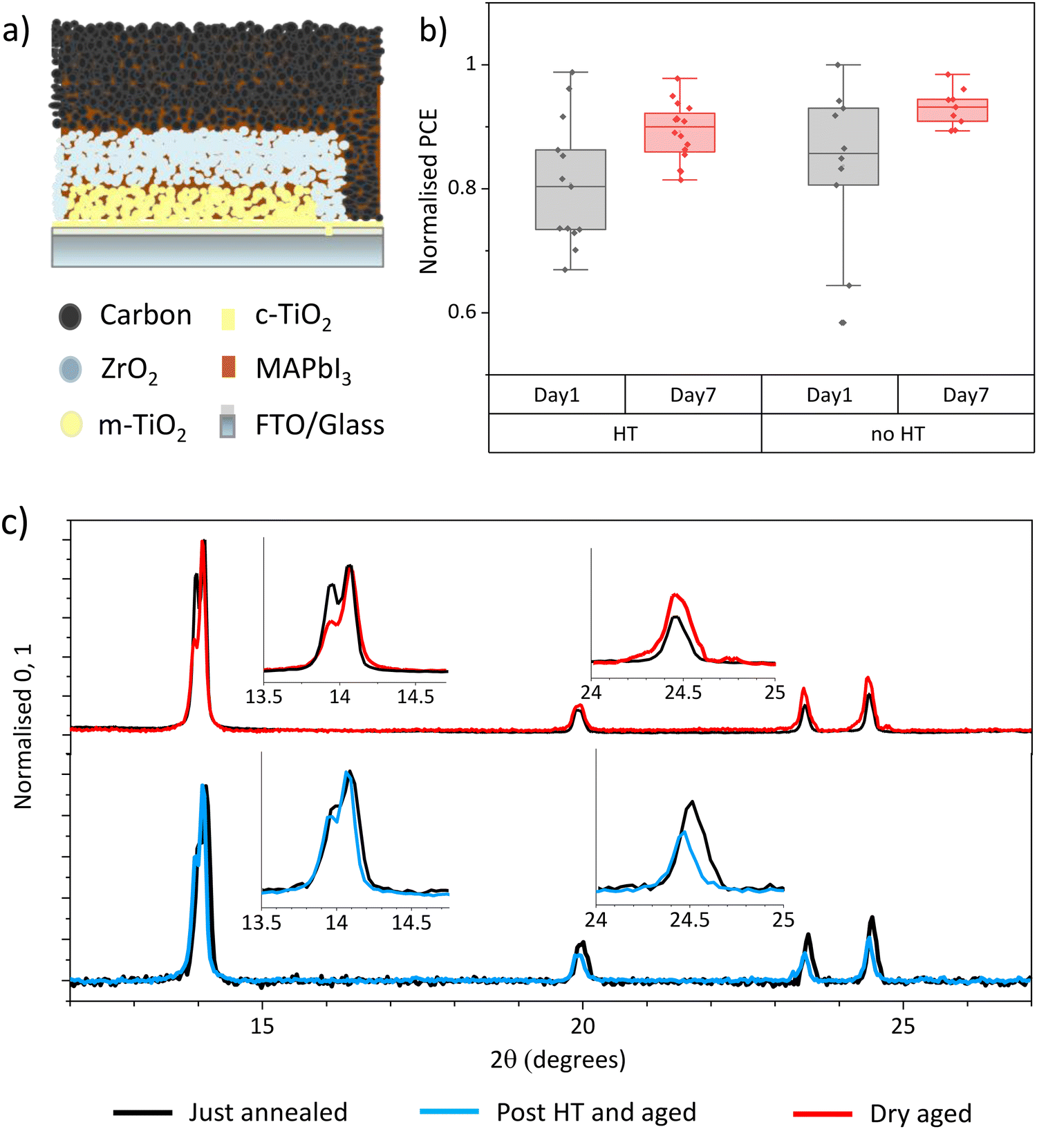 | ||
| Fig. 1 (a) Diagrammatic representation of a CPSC cross section. (b) Normalised PCEs of GVL CPSCs before and after HT or dry ambient storage. Samples were measured 1 day and 7 days after fabrication, with HT on days 2–3. 14–18 samples in each set. (c) XRD of AVA0.03MAPbI3 perovskites crystallised from GVL-based precursors in mesoporous ZrO2 scaffolds. Samples were examined directly after annealing (black) and again after exposure to dry ambient air (red) or 70% RH HT (blue). | ||
Previous work has found that MAPbI3 crystallised from GVL in mesoporous scaffolds is of superior crystallinity to similar samples crystallised from GBL.20 Cells fabricated using DMF/DMSO or NMF precursors with high initial crystallinity achieve high PCE without HT.16,17 It was therefore unknown whether HT would have an impact on GVL samples.
To thoroughly examine the impact of humidity on GVL cells, devices were made and split into two groups immediately following manufacture. Devices are printed in strips of four cells. To avoid print variations causing a misleading trend, devices were grouped to ensure an even mix of prints from each strip in each batch. One group was then subjected to a 24 hour HT and the other to dry ambient exposure (≤20% RH). After HT, devices from were stored in dry ambient conditions before remeasurement. To monitor any changes in perovskite crystallinity, XRD measurements were performed before and after humidity or dry ambient exposure.
Fig. 1(b) shows normalised PCEs of GVL devices before and after HT or dry storage. Non normalised data is presented in Fig. S1 (ESI†). The non-HT sample group tested slightly higher than those from HT on day 1 due to high variation between samples. Both groups of devices experienced similar performance improvements over time due to Voc and FF increases (Fig. S1, ESI†), resulting in a higher overall performance in the non-HT group. It is clear from these data that GVL devices improve over time regardless of humidity exposure. Another variable must therefore be causing this change.
Light and age related PCE increases In DMF/DMSO cells have been assigned to complex ion rearrangement at electrode interfaces.17 Conversely, in GBL devices, HT improves PCE through inducing crystallinity and orientation changes, Fig. S2 and S3 (ESI†).11,14 This can be observed in Fig. S3 (ESI†), where HT GBL samples show reorientation towards the (110) plane and dry stored cells remain unchanged.
Fig. 1(c) shows the XRD spectra of GVL devices before and after HT or dry storage, which show clear changes in perovskite orientation over time in both samples. As in the case of GBL, the HT sample realigned to favour the (110) = orientation with a 14° dominant peak.12,21 Conversely, the dry sample reoriented away from a (110) alignment, with other peaks increasing in relative intensity.
These results suggest that, like in GBL cells, perovskite crystallised from GVL can undergo significant changes that positively impact performance after annealing. However, this is occurring independently of humidity exposure in GVL cells, which has is not observed in the case of GBL.
3.2. Examining performance evolution in dry-ambient stored devices
To ascertain that changes were reproducible between batches and more closely examine the extent of performance changes under dry ambient storage, a more comprehensive study was undertaken.Fig. 2(a) shows the photovoltaic performance parameters of standard control devices from eight different experiments 1 day and 7 days post-infiltration. Each device was carefully marked prior to testing to ensure identical mask placement across multiple tests. Performance changes were also examined at an individual level, by calculating the % change of each photovoltaic parameter for each device over time. It should be noted that the initial batch also tested on day 4, but cells had not yet reached peak performance (Fig. S3, ESI†). The long time frame therefore appears necessary for achieving peak performance.
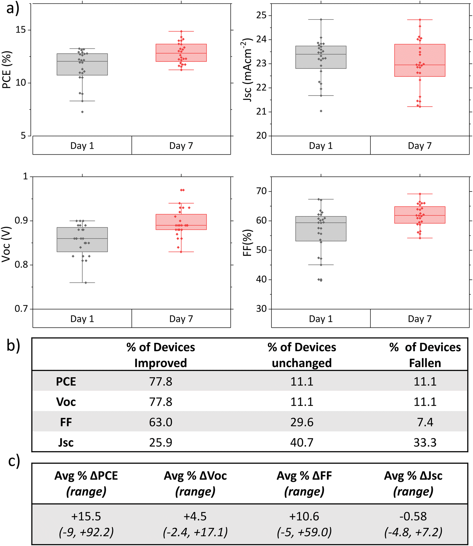 | ||
| Fig. 2 (a) PV parameters of 27 GVL AVA0.03MAPbI3 devices from various batches, 1 and 7 days after fabrication. (b) Table showing % of devices that experienced an improvement, no change, or fall in performance. (c) Table showing average and range % change in each PV parameter compared to initial values. | ||
A clear increase in PCE over time was observed in 78% of devices (Fig. 2(a) and (b)). The extent of this performance change was extremely varied, ranging from 7% to 92.2% improvement on the initial performance (average change 15.5%, Fig. 2(c)). 11% of devices showed no change, with the remaining 11% falling compared to the initial measurement. Devices that fell in performance did not show a drastic decrease, with a maximum decrease of 7% of initial PCE observed.
Overall, there is a clear time-dependent increase in performance driven primarily by the FF and Voc: 78% of devices experiencing a Voc increase (mean +5%, maximum +20%), and 63% improved FF (mean +10.6%, maximum +58%). On average, Jsc remained statistically similar between measurements, with a mean change of well below 1% over time.
This represents a key difference to the performance increases seen in GBL and DMF/DMSO devices examined in other works, where large Jsc improvements were the main contributor to PCE enhancement.11,14,17 Significant Voc changes were highlighted in these works only after light and bias exposure treatments.14,17 This suggests that the underlying mechanism behind PCE gains may be different in this case.
V oc and FF enhancements are respectively indicative of improved carrier lifetime and better charge extraction.22,23 This corroborates the crystallinity changes observed with XRD: greater crystal alignment has been shown to improve Voc in MAPbI3 devices.22,24–26
While the XRD measurements above showed crystallinity changes over time, this measurement only provides information about perovskite atop or within the carbon electrode. This may not represent the behaviour of perovskite deeper within the stack. Therefore, to examine perovskite properties within the TiO2 layer, photoluminescence (PL) and photocurrent (PC) maps were obtained.
Fig. 3(a)–(c) show PL, PC and PL peak position maps of the TiO2 layer of an infiltrated device obtained 1 day and 7 days after perovskite annealing, alongside concurrent device performance (Fig. 3(d)).
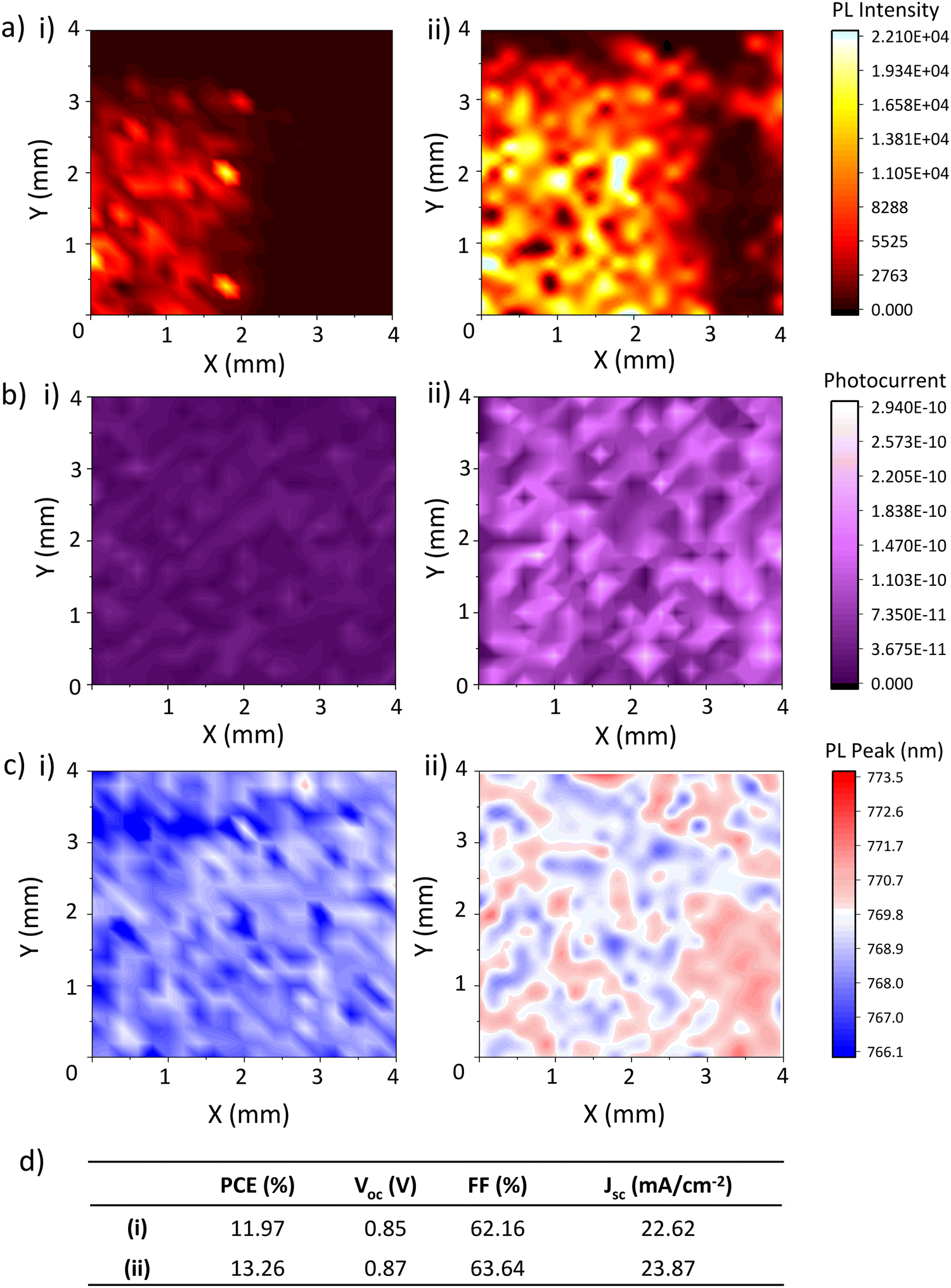 | ||
| Fig. 3 (a) Photoluminescence maps, (b) Photocurrent maps, (c) PL peak position maps, and (d) PV performance parameters of a device 1 (i) and 8 (ii) days after fabrication. | ||
Alongside device PCE, FF, Voc and performance increases, PL intensity (Fig. 3(a)) rose significantly between measurements, from 1620 average counts on day 1 to 8064 on day 7. Lower emission intensity is observed at the right of the sample, likely due to closer proximity to the carbon electrode.
PL intensity correlates positively with crystal quality, with larger more crystalline samples producing more intense emission due to lower levels of recombination.27–29 This large PL increase is likely indicative of a significant decrease in non-radiative recombination across the active area, which suggests some form of defect passivation is occurring. This would be consistent with the perovskite crystal realignment observed in Fig. 1.21,27,30 Although PL at the base of a cell could also indicate that perovskite-TiO2 contact is poorer in day 7 samples due to reduced PL quenching, improved device FF and PCE with on day 7 suggest the opposite is true.
A significant change in PC also occurred between days one and seven, increasing tenfold in the second measurement (Fig. 3(b)). However, IV results did not reflect this- although device Jsc improved slightly, the change was not particularly drastic. This discrepancy is likely due to differences in the IV and PL mapping testing setup. The IV results presented in this work were all obtained after three minutes of light soaking, required in CPSCs because the thick mesoscopic stack restricts ion movement and increases the distance across which carriers must travel.28,29 However, such light soaking is not possible with the low intensity, small spot size laser used for PL and PC mapping.
The PC measured during mapping is therefore more representative of device response during light soaking. A much higher photocurrent being generated during mapping is likely therefore due to faster response under illumination as opposed to increased steady state current output. This is typical of improved perovskite quality, where fewer shallow traps and improved charge transport result in faster current generation.26,27
Interestingly, PL redshifts were also observed with ageing (Fig. 3(c)). This was somewhat unexpected: crystal realignments and associated defect passivation was expected to cause a blue-shift due to a reduction in shallow traps increasing the optical bandgap. Although this could be an indication of early degradation, this was considered unlikely as device performance had significantly improved and aged XRD samples contained no sign of PbI2 formation (Fig. 1).
Some works have shown that perovskite crystallite size can impact PL peak position, with larger crystallites producing a redshifted emission peak.31,32 Similar claims have been made about crystal orientation.33 However, several conflicting studies show that grain size and orientation have no significant impact on PL emission wavelength.33 Therefore, while the redshift observed here may indicate some recrystallisation, it cannot by itself conclusively identify this as the cause. Alternatively, the crystal reorganisation observed in the XRD could passivate non-radiative deep traps, producing perovskite with a shallower trap population and thus increased, redshifted PL emission after 7 days.
It is clear from the changes in PL and PC data that significant changes are occurring at the base of the stack over time. This indicates that the observed perovskite crystallinity changes are consistent throughout the device, lowering non-radiative recombination and increasing device Voc.
The drastic increase in device PC response suggests that interfacial charge transfer is also impacted. To further examine this, electrochemical impedance spectroscopy (EIS) was therefore performed on cells on days 1 and 7 to examine whether interfacial charge extraction changes over time.
As CPSCs contain many complex interfaces, there is currently little agreement on detailed interpretation of EIS data, with 2, 3 and 4 equivalent electrical circuit diagrams presented in the literature.34–36 There is however some consensus that the high and upper intermediate frequency regions are respectively associated with carbon/perovskite and TiO2/perovskite interfacial charge transfer, while the area of the first Nyquist arc has been related to charge transfer resistance (RCT) in several works.34–36 Shifts in the size and position of this large arc are therefore indicative of changes in interfacial charge transfer and overall series resistance.32,35
Fig. 4 presents Nyquist impedance plots of the fresh and aged device. A large arc from the high to intermediate frequency region is evident in both devices, with additional features towards the low frequency region.
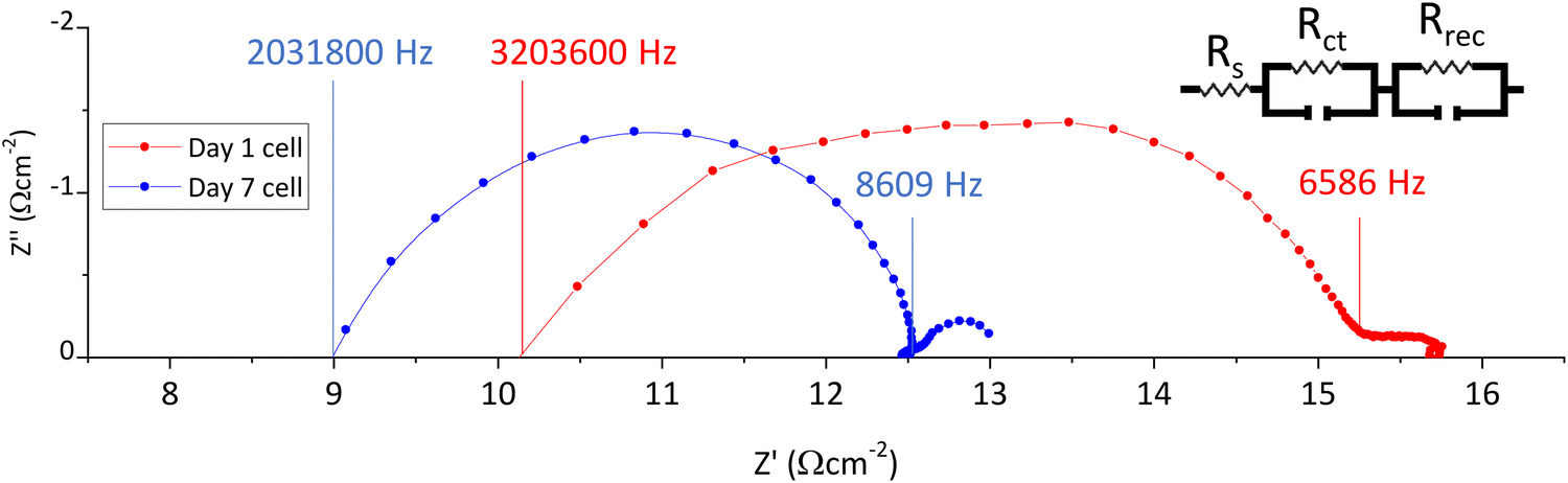 | ||
| Fig. 4 Nyquist plots of a cell on days 1 and 7, with relevant frequencies labelled for the start and end points of the large first arc. | ||
Both the high and intermediate frequency regions of the day 7 Nyquist curve in Fig. 4 are shifted to much lower values, indicating that perovskite-electrode charge transfer is superior at both electrodes after ageing. This csonfirms that the increased PL observed in Fig. 3 is not due to poorer perovskite contact in this sample and supports the conclusion that the increase in photocurrent is a consequence of faster device response (due to improved perovskite-electrode contact).32
3.3. Determining the cause of performance increases
It is clear that device performance improves under dry ambient conditions over the week following fabrication. Previous work has shown that light exposure can induce changes in perovskite crystal structure, resulting in irreversible Voc enhancements.37,38 Bias application can also induce structural changes.37 It was therefore posited that some element of the device testing process could be driving the observed performance increases.An experiment was therefore devised to determine whether IV testing was driving performance evolution. This is visually depicted in Table 1. After perovskite annealing, devices were split into four groups, with group 1 tested as usual, group 2 exposed only to testing bias sweeps, group 3 only to light and group 4 to dark storage. Should PCE increases be related to light exposure or bias, the untested dark storage samples will exhibit lower PCE upon testing on day 7.
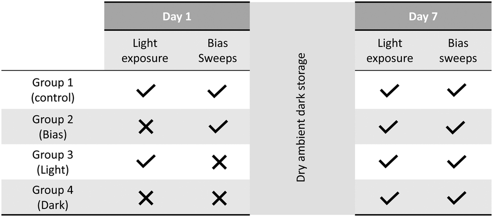
|
All samples exhibited similar performance on day 7 (Fig. S4, ESI†), indicating that performance enhancements were occurring independently of light or bias exposure.
Having eliminated the testing process as a cause of these changes, two potential causes of performance enhancement remain. It is possible that crystal realignment occurs spontaneously, as realignment to reduce strain may be energetically favourable. Alternatively, environmental exposure could be causing the change, as all data presented thus far were from unencapsulated devices stored in dry ambient (≤20% RH) environments. Although humidity exposure was not found to influence performance enhancements in Fig. 1, keeping devices unencapsulated allows potential ingress of other environmental species such as O2, as well as egress of internal components such as residual solvent or volatile MAI. Should such a process be causing the observed changes, early encapsulation to isolate the device from the surrounding environment should inhibit PCE improvements.
As shown in Fig. S5 (ESI†), encapsulated devices did not improve over time, remaining the same after encapsulation before falling in performance by day. On average, this was driven by losses in Jsc, with Voc and FF losses also observed in several samples (Fig. S5 and Table S1, ESI†). Each individual encapsulated device suffered some loss in performance between days 3 and 8, while unencapsulated controls improved as observed in previous batches (Table S2, ESI†).
Not allowing environmental exposure following fabrication not only prevented performance enhancement but induced significant Voc and FF losses. It appears that an ageing period where devices are left unencapsulated is required to ensure high performance and stability. This could be a critical consideration in potential scale-up settings, where completed devices are typically encapsulated immediately following fabrication.
Clearly, something must enter or exit the stack following fabrication to achieve peak performance. Previous work has revealed that significant amounts of solvent can remain in perovskite films after annealing, even in planar devices with no evaporation-limiting scaffold.39–41 While GVL has a high boiling point of 208 °C, CPSCs are annealed at 45 °C to slow crystal nucleation and promote high quality infiltration. GVL is clearly removed at this temperature, as crystallisation to the black phase occurs. However, residual solvent may remain- especially deep in the base TiO2 layer where microns of scaffold restrict solvent escape.
Recent work showed that ethylene carbonate additives remain in AVA0.03MAPbI3 CPSCs after annealing, coordinating to Pb centres via the carbonyl group.42 As a structurally similar compound, GVL could also interact with Pb centres and grain boundary iodide vacancy defects through its electron rich C![[double bond, length as m-dash]](https://www.rsc.org/images/entities/char_e001.gif) O group. This could further prevent solvent removal during annealing. To observe whether GVL could remain after annealing and identify any coordination to Pb centres, Fourier transform infrared (FTIR) spectroscopy was performed.
O group. This could further prevent solvent removal during annealing. To observe whether GVL could remain after annealing and identify any coordination to Pb centres, Fourier transform infrared (FTIR) spectroscopy was performed.
Fig. 5(a) shows FTIR spectra of pure GVL, pure PbI2 and PbI2 dried from a GVL suspension for an hour at 45 °C (reflecting a typical perovskite annealing procedure). FTIR comparisons of perovskites were not performed, as the organic groups and AVA COOH sections would likely mask any signals due to residual GVL. A table of identified major peaks is available in Table S3 (ESI†).
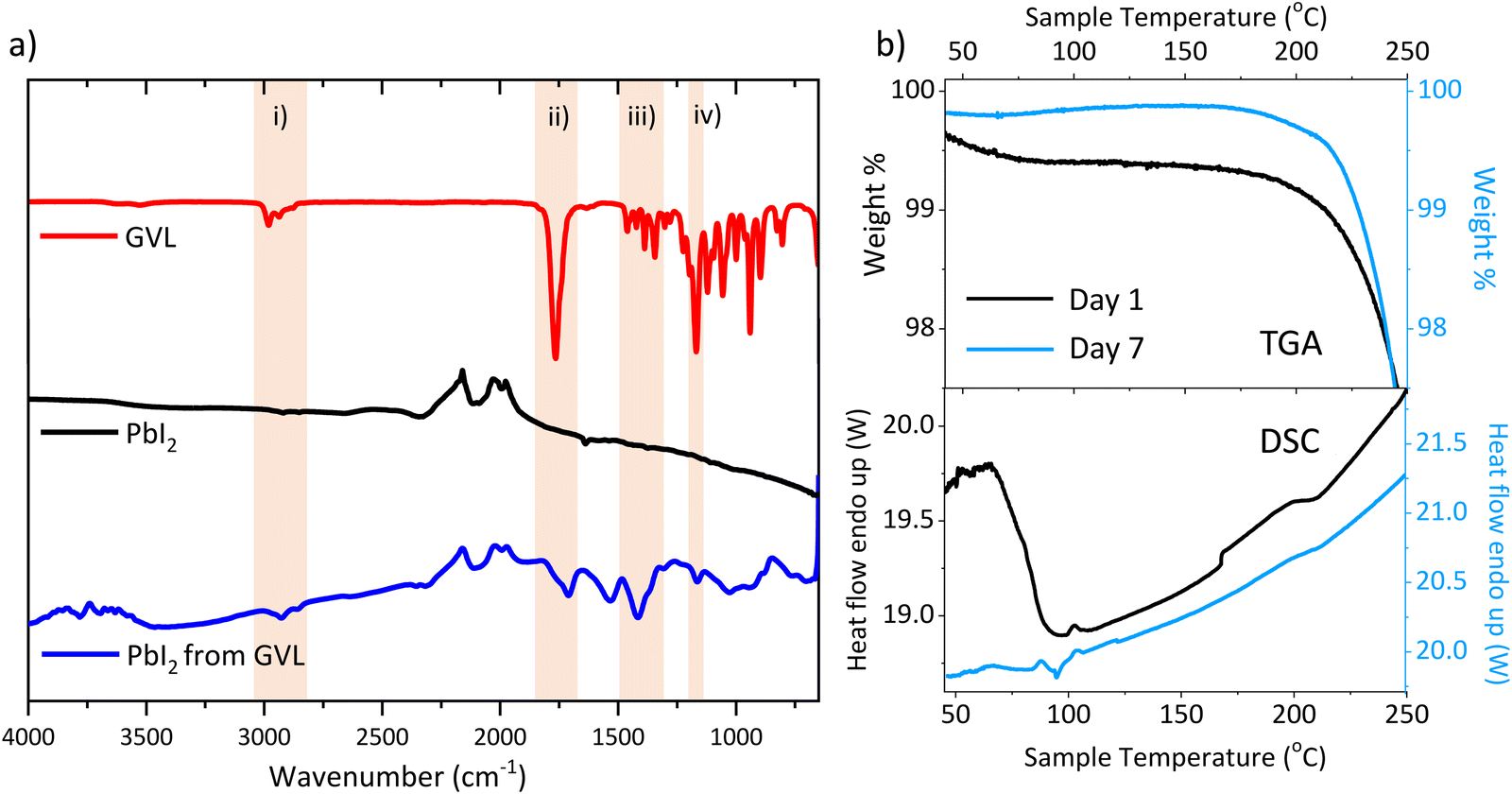 | ||
| Fig. 5 (a) FTIR of pure GVL, pure PbI2 and PbI2 after drying from GVL at 45 °C. Highlighted sections show notable characteristic GVL peaks, identified in Table S3 (ESI†). (b) TGA, derivative weight % and DSC of AVA0.03MAPbI3 in ZrO2 24 h (i) and 7 days (ii) after annealing. | ||
The pure GVL sample showed a clear sharp symmetric CO stretch at 1762 cm−1, as well as a group of C–H stretches at 2800–3000 cm−1, respectively representing the lactone group and hydrocarbon backbone. These peaks are also present in the dried GVL-PbI2 sample and absent in the pure PbI2. This indicates that the perovskite annealing process did not fully remove GVL from the PbI2.
Interestingly, the dried GVL-PbI2 CO peak shifted to 1710 cm−1 and presented with shoulder towards higher wavenumbers. Such a shift can be indicative of CO interaction with a metal centre, although the presence of a shoulder suggests that some uncoordinated GVL may also reside in the film.43 An O-H stretch at ∼3000–3500 cm−1 was also present in the dried GVL-PbI2 trace. While this could be evidence of GVL ring opening, this was considered improbable as such reactions generally occur in the presence of water and a catalyst.44 It is more likely due to ambient water adsorption, as samples were stored briefly in ambient air (∼55% RH) prior to measuring.
As annealing at 45 °C for an hour did not fully remove GVL from PbI2, and there is evidence of coordination to Pb centres, it is likely that it is also retained after perovskite annealing in devices. It was posited that slow residual solvent loss over time may therefore account for the observed crystallinity and performance changes.
To determine whether GVL was retained in annealed perovskite, thermogravimetric analysis (TGA) and differential scanning calorimetry (DSC) were performed on fresh and aged AVA0.03MAPbI3 in ZrO2 scaffolds, to mimic the conditions in a cell.
In accordance with previous studies, TGA showed a large loss from 200–300 °C comprised of two separate events, a smaller loss from 225–250 °C is also present likely AVA removal, followed by a much larger MAI loss (Fig. S6, ESI†).38
Critically, Fig. 5(b) reveals a 0.5% initial mass loss in the day 1 sample from 40–100 °C. This is accompanied by an endothermic DSC peak in the same temperature range and is typical of residual solvent loss.38,42 No such TGA loss is present in the day 7 data, and no endothermic DSC peak is observed, indicating that the retained solvent is no longer present. The residual solvent must therefore be leaving the stack during this period, which could drive the observed changes in perovskite crystallinity and device behaviour.
A long ageing period to allow slow recrystallisation over several days is not practical, especially from a commercial standpoint. Residual GVL could be removed by using a higher annealing temperature, however, this risks detrimentally fast crystallisation. Therefore, device annealing time was increased from one hour to 2.5 hours in an attempt to remove all solvent during the initial fabrication.
Presented in Fig. 6, long annealed samples did not exhibit higher initial performance, and also displayed limited performance enhancement over the week when compared to standard devices. It would appear that removing a greater proportion of solvent at the outset did not produce enhanced crystallinity, and furthermore limited the capacity for crystal reorganisation following fabrication.
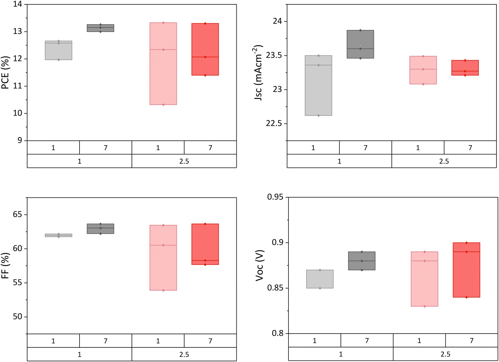 | ||
| Fig. 6 Performance of GVL-MeOH AVA0.03MAPbI3 devices annealed for 1 or 2.5 hours at 45 °C 1 day and 7 days after fabrication. Four samples in each set. | ||
It therefore seems that the slow loss of solvent over time is key to maximising performance in this case, as devices encapsulated early or exposed to greater annealing time do not improve after fabrication. An ageing period to enable residual solvent loss and crystal realignment is therefore advised prior to encapsulation of CPSCs or modules made using GVL precursors. It should be noted that this may also occur with other precursor solvents: CPSCs are generally infiltrated with high boiling point solvents (i.e. DMF, DMSO, GBL), but annealed at low temperatures of <100 °C to aid infiltration.43
4. Performance increases in modules
To ascertain whether similar performance increases occur at large scale, three 220 cm2 active area modules were fabricated and measured on days 1 and 7 after infiltration. Photovoltaic parameters are shown in Fig. 7.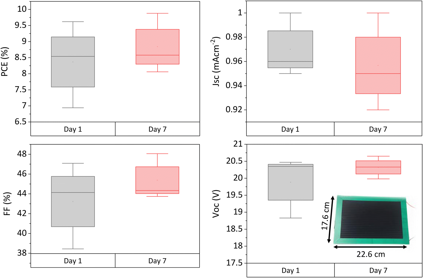 | ||
| Fig. 7 Photovoltaic parameters of 220 cm2 modules 1 and 7 days after infiltration. 3 modules tested. Inlaid photograph of a module with substrate measurements. | ||
Performance enhancement was observed in two of the three samples, with the third showing a negligible change. As in smaller cells, this was due to improvements in Voc and FF, while Jsc had a negligible change. The PCE increased by 6.44% on average, slightly less than in the small devices (which improved by 15.5% PCE on average). Average batch PCE was Improvements in crystal quality due to residual solvent loss may be having less impact on performance here due to the greater detrimental impact of the non-selective carbon electrode at scale. Therefore, as performance is more limited by factors such as series resistance, recrystallisation may have less of an impact.
However, as performance increases were still observed over time, residual solvent is likely still present in freshly infiltrated modules. To attain peak performance and prevent detrimental lifetime losses, modules should therefore be left post fabrication to allow time for residual solvent removal before encapsulation.
5. Conclusion
This work examines the performance evolution of CPSCs made using GVL-based precursors. Although similar GBL and DMF/DMSO cells are respectively known to benefit from humidity and light treatments, GVL devices improve over time regardless of humidity application. Increases in FF and Voc drive significant performance increases in 78% of devices following fabrication, with an average gain of 15.5% on the initial PCE. This was also observed at larger scale, with 220 cm2 modules experiencing a 6.4% PCE increase. This is a consequence of slow loss of residual solvent, which enables crystal reorientation without post treatment, evidenced by concurrent XRD peak ratio PL intensity changes.Crucially, early device encapsulation and long-annealing were found to reduce initial performance and hinder PCE improvements. Preventing solvent egress and the related crystal reorganisation during the ageing period is therefore detrimental to both performance and lifetime. A period of unencapsulated storage is therefore recommended prior to encapsulation to attain peak cell or module performance. This work may enable improved laboratory results using GVL precursors and could aid in designing scaled-up processes for fabricating high performing CPSC modules.
Conflicts of interest
We have no conflict of interest to disclose.Acknowledgements
This work was made possible by support from the Royal Society International Collaboration award (ICA\R1\191321) and the Newton Fund Impact Scheme (541128962). Additional support was received via the EPSRC Programme Grant ATIP (Application Targeted and Integrated Photovoltaics) (EP/T028513/1) and the SPECIFIC Innovation and Knowledge Centre (EP/N020863/1), Innovate UK (920036) and European Regional Development Fund (c80892) through the Welsh Government. Data is available upon request from the author.References
- Z. Ku, Y. Rong, M. Xu, T. Liu and H. Han, Sci. Rep., 2013, 3, 3132 CrossRef PubMed.
- A. Mei, X. Li, L. Liu, Z. Ku, T. Liu, Y. Rong, M. Xu, M. Hu, J. Chen, Y. Yang, M. Gratzel and H. Han, Science, 2014, 345, 295–298 CrossRef CAS PubMed.
- C.-T. Lin, F. De Rossi, J. Kim, J. Baker, J. Ngiam, B. Xu, S. Pont, N. Aristidou, S. A. Haque, T. Watson, M. A. McLachlan and J. R. Durrant, J. Mater. Chem. A, 2019, 7, 3006–3011 RSC.
- E. V. Péan, C. S. De Castro, S. Dimitrov, F. De Rossi, S. Meroni, J. Baker, T. Watson and M. L. Davies, Adv. Funct. Mater., 2020, 1909839 CrossRef.
- A. Mei, Y. Sheng, Y. Ming, Y. Hu, Y. Rong, W. Zhang, S. Luo, G. Na, C. Tian, X. Hou, Y. Xiong, Z. Zhang, S. Liu, S. Uchida, T.-W. Kim, Y. Yuan, L. Zhang, Y. Zhou and H. Han, Joule, 2020, 4, 2646–2660 CrossRef CAS.
- K. Knudsen, J. Greter and M. Verdicchio, Clin. Toxicol., 2008, 46, 187–192 CrossRef CAS PubMed.
- Gamma-butyrolactone (GBL) Pre-Review Report Expert Committee on Drug Dependence Thirty-fifth Meeting, World Health Organisation, 2012.
- GBL MSDS - B103608, https://www.sigmaaldrich.com/MSDS/MSDS/DisplayMSDSPage.do?country=GB&language=en&productNumber=B103608&brand=ALDRICH&PageToGoToURL=https%3A%2F%2Fwww.sigmaaldrich.com%2Fcatalog%2Fproduct%2Faldrich%2Fb103608%3Flang%3Den, (accessed 16 March 2020).
- F. Kerkel, M. Markiewicz, S. Stolte, E. Müller and W. Kunz, Green Chem., 2021, 23, 2962–2976 RSC.
- A. Kumar, A. Sharma, B. G. de la Torre and F. Albericio, Molecules, 2019, 24, 4004 CrossRef CAS PubMed.
- A. Osatiashtiani, A. F. Lee and K. Wilson, J. Chem. Technol. Biotechnol., 2017, 92, 1125–1135 CrossRef CAS.
- S. G. Hashmi, D. Martineau, M. I. Dar, T. T. T. Myllymäki, T. Sarikka, V. Ulla, S. M. Zakeeruddin and M. Grätzel, J. Mater. Chem. A, 2017, 5, 12060–12067 RSC.
- A. Karavioti, E. Vitoratos and E. Stathatos, J. Mater. Sci.: Mater. Electron., 2020, 1–9 Search PubMed.
- F. De Rossi, J. A. Baker, D. Beynon, K. E. A. Hooper, S. M. P. Meroni, D. Williams, Z. Wei, A. Yasin, C. Charbonneau, E. H. Jewell and T. M. Watson, Adv. Mater. Technol., 2018, 3, 1800156 CrossRef.
- S. G. Hashmi, D. Martineau, X. Li, M. Ozkan, A. Tiihonen, M. I. Dar, T. Sarikka, S. M. Zakeeruddin, J. Paltakari, P. D. Lund and M. Grätzel, Adv. Mater. Technol., 2017, 2, 1600183 CrossRef.
- Q. Wang, W. Zhang, Z. Zhang, S. Liu, J. Wu, Y. Guan, A. Mei, Y. Rong, Y. Hu and H. Han, Adv. Energy Mater., 2020, 10, 1903092 CrossRef CAS.
- S. Liu, Y. Sheng, D. Zhang, W. Zhang, Z. Qin, M. Qin, S. Li, Y. Wang, C. Gao, Q. Wang, Y. Ming, C. Liu, K. Yang, Q. Huang, J. Qi, Q. Gao, K. Chen, Y. Hu, Y. Rong, X. Lu, A. Mei and H. Han, Fundam. Res., 2021, 2, 276–283 CrossRef.
- C. Ling, Y. Xia, X. Xiao, X. Chen, Z. Zheng, M. Xia, Y. Hu, A. Mei, Y. Rong and H. Han, Small Methods, 2022, 6, 2200161 CrossRef CAS PubMed.
- Y. Cheng, Z. Zheng, S. Liu, J. Xiang, C. Han, M. Xia, G. Zhang, J. Qi, Y. Ma, K. Chen, Y. Tao, X. Lu, A. Mei and H. Han, Adv. Energy Mater., 2023, 14, 2303988 CrossRef.
- C. Worsley, D. Raptis, S. Meroni, A. Doolin, R. Garcia, M. Davies and T. Watson, Energy Technol., 2021, 9, 2100312 CrossRef CAS.
- Y. Rong, X. Hou, Y. Hu, A. Mei, L. Liu, P. Wang and H. Han, Nat. Commun., 2017, 8, 14555 CrossRef PubMed.
- T. Du, J. Kim, J. Ngiam, S. Xu, P. R. F. Barnes, J. R. Durrant and M. A. McLachlan, Adv. Funct. Mater., 2018, 28, 1801808 CrossRef.
- A. Bashir, J. H. Lew, S. Shukla, D. Gupta, T. Baikie, S. Chakraborty, R. Patidar, A. Bruno, S. Mhaisalkar and Z. Akhter, Sol. Energy, 2019, 182, 225–236 CrossRef CAS.
- J. Wu, W. Zhang, Q. Wang, S. Liu, J. Du, A. Mei, Y. Rong, Y. Hu and H. Han, J. Mater. Chem. A, 2020, 8, 11148–11154 RSC.
- C. M. Tsai, G. W. Wu, S. Narra, H. M. Chang, N. Mohanta, H. P. Wu, C. L. Wang and E. W. G. Diau, J. Mater. Chem. A, 2017, 5, 739–747 RSC.
- H. Lakhiani, T. Dunlop, F. De Rossi, S. Dimitrov, R. Kerremans, C. Charbonneau, T. Watson, J. Barbé and W. C. Tsoi, Adv. Funct. Mater., 2019, 29, 1900885 CrossRef.
- E. V. Péan, C. S. De Castro and M. L. Davies, Mater. Lett., 2019, 243, 191–194 CrossRef.
- K. P. Goetz, A. D. Taylor, F. Paulus and Y. Vaynzof, Adv. Funct. Mater., 2020, 30, 1910004 CrossRef CAS.
- M. Abdi-Jalebi, Z. Andaji-Garmaroudi, S. Cacovich, C. Stavrakas, B. Philippe, J. M. Richter, M. Alsari, E. P. Booker, E. M. Hutter, A. J. Pearson, S. Lilliu, T. J. Savenije, H. Rensmo, G. Divitini, C. Ducati, R. H. Friend and S. D. Stranks, Nature, 2018, 555, 497–501 CrossRef CAS PubMed.
- S. Jariwala, H. Sun, G. W. P. Adhyaksa, A. Lof, L. A. Muscarella, B. Ehrler, E. C. Garnett and D. S. Ginger, Joule, 2019, 3, 3048–3060 CrossRef CAS.
- V. D’Innocenzo, A. R. Srimath Kandada, M. De Bastiani, M. Gandini and A. Petrozza, J. Am. Chem. Soc., 2014, 136, 17730–17733 CrossRef PubMed.
- A. Ummadisingu, S. Meloni, A. Mattoni, W. Tress and M. Grätzel, Angew. Chem., Int. Ed., 2021, 60, 21368–21376 CrossRef CAS PubMed.
- L. A. Muscarella, E. M. Hutter, S. Sanchez, C. D. Dieleman, T. J. Savenije, A. Hagfeldt, M. Saliba and B. Ehrler, J. Phys. Chem. Lett., 2019, 10, 6010–6018 CrossRef CAS PubMed.
- S. M. Abdulrahim, Z. Ahmad, J. Bahadra and N. J. Al-Thani, Nanomaterials, 2020, 10, 1635 CrossRef CAS PubMed.
- Z. Ahmad, A. Mishra, S. M. Abdulrahim and F. Touati, J. Electroanal. Chem., 2020, 871, 114294 CrossRef CAS.
- Y. Yang, K. Ri, A. Mei, L. Liu, M. Hu, T. Liu, X. Li and H. Han, J. Mater. Chem. A, 2015, 3, 9103–9107 RSC.
- A. Schneider, S. Alon and L. Etgar, Energy Technol., 2019, 1900481 CrossRef.
- E. Kobayashi, R. Tsuji, D. Martineau, A. Hinsch and S. Ito, Cell Rep. Phys. Sci., 2021, 2, 100648 CrossRef CAS.
- A. E. Williams, P. J. Holliman, M. J. Carnie, M. L. Davies, D. A. Worsley and T. M. Watson, J. Mater. Chem. A, 2014, 2, 19338–19346 RSC.
- Y. K. Ren, S. D. Liu, B. Duan, Y. F. Xu, Z. Q. Li, Y. Huang, L. H. Hu, J. Zhu and S. Y. Dai, J. Alloys Compd., 2017, 705, 205–210 CrossRef CAS.
- Y. Zhou, A. Najar, J. Zhang, J. Feng, Y. Cao, Z. Li, X. Zhu, D. Yang and S. F. Liu, ACS Appl. Mater. Interfaces, 2022, 14, 28729–28737 CrossRef CAS PubMed.
- D. Bryant, N. Aristidou, S. Pont, I. Sanchez-Molina, T. Chotchunangatchaval, S. Wheeler, J. R. Durrant and S. A. Haque, Energy Environ. Sci., 2016, 9, 1655–1660 RSC.
- K. Chen, Z. Zhang, J. Liu, Y. Huang, D. Wang, B. She, B. Liu, X. Zhang and J. Zhang, Adv. Mater. Interfaces, 2022, 9, 2100395 CrossRef CAS.
- R. Pothu, R. Gundeboyina, R. Boddula, V. Perugopu and J. Ma, New J. Chem., 2022, 46, 5907–5921 RSC.
Footnote |
| † Electronic supplementary information (ESI) available. See DOI: https://doi.org/10.1039/d4ma00136b |
| This journal is © The Royal Society of Chemistry 2024 |