
 Open Access Article
 This Open Access Article is licensed under a Creative Commons Attribution-Non Commercial 3.0 Unported Licence
Low-temperature curable TiO2 sol for separator and HTM-free carbon-based perovskite solar cells†
Reshma Dileep
K
ab,
Thulasi Raman
Elumalai
a,
Easwaramoorthi
Ramasamy
 a,
S.
Mallick
b,
T. N.
Rao
a and
Ganapathy
Veerappan
*a
a,
S.
Mallick
b,
T. N.
Rao
a and
Ganapathy
Veerappan
*a
aCenter for Solar Energy Materials, International Advanced Research Center for Powder Metallurgy and New Materials (ARCI), Balapur PO, Hyderabad 500005, Telangana, India. E-mail: ganagv@arci.res.in
bDepartment of Metallurgical Engineering & Materials Science, Indian Institute of Technology, Bombay, Powai, Mumbai 400076, Maharashtra, India
First published on 26th September 2023
Abstract
In this study, we present the development of an ambient temperature curable TiO2 mesoporous layer for perovskite solar cells (PSCs), eliminating the need for a binder and enabling the use of environmentally friendly solvents. The TiO2 layer was synthesized via a hydrothermal method followed by minimal post-processing techniques. The resulting anatase TiO2 sol was optimized to be compatible with various coating techniques such as spin coating, dip coating, and spray coating, allowing for its application at sub-50 °C temperatures. A comprehensive investigation was conducted to study the effects of annealing temperatures ranging from 50 °C to 500 °C on the crystallographic, morphological, electrical, and surface properties of the TiO2 films derived from the TiO2 sol. Contact angle measurements were employed to analyse the change in surface energy resulting from different sintering temperatures and its influence on the growth of the perovskite film on the TiO2 films. To evaluate the performance of the TiO2 electron transport layers (ETLs) annealed at different temperatures, carbon-based perovskite solar cells (CPSCs) were fabricated. The results revealed that the CPSCs utilizing the TiO2 ETL annealed at 50 °C exhibited the highest efficiency of 11.1%, accompanied by an open circuit voltage of 0.98 V and a current density of 22.3 mA cm−2. Notably, the developed TiO2 ETL outperformed the commercial TiO2 ETL sintered at 500 °C in the same device architecture. These findings demonstrate the potential of the ambient temperature curable TiO2 ETL for large-area deposition and flexible PSCs.
Introduction
The use of renewable energy resources is shifting to high gears as a result of the depleting non-renewable resources. The Sun is the most extensively harnessed renewable energy source, in the form of solar photovoltaic and solar thermal energy. Among various photovoltaic technologies, perovskite solar cells (PSCs) have proved to be promising due to their high power conversion efficiencies (PCEs), low-cost, and facile fabrication techniques. Perovskite absorbers are of high interest due to their outstanding intrinsic properties, such as tunable band gap over a large range, high absorption coefficient, long diffusion length, ambipolar charge transport, etc.1 For photovoltaic applications, perovskite material (MaPbI3) was first used in 2009 to replace the absorber material in a dye sensitized solar cell, and an efficiency of 3.8% was reported.2 Though the PSCs were short-lived, this paved the way for a new class of solar cells. Various research groups carried out intense optimization around the world in material engineering, interface engineering, device architecture, optimization of various device fabrication steps, etc.,3 which rendered an unprecedented improvement in the stability and photovoltaic performance of the PSCs.Carbon based HTM-free PSCs (CPSCs) are one of the successful device architectures that circumvent the stability aspect as well as the cost of fabrication in a conventional PSC. CPSCs generally use the triple mesoscopic architecture (TiO2/ZrO2/perovskite/carbon), where TiO2 is the electron transport layer (m-TiO2), and mesoporous ZrO2 or Al2O3 is used as the separator layer, with a carbon cathode.4 The m-TiO2 and the ZrO2 layers require high temperature sintering, which increases the energy payback time, rendering the device fabrication process extensive and also limiting the usage of flexible polymer substrates. Another challenge in triple mesoscopic CPSCs is the perovskite infiltration, where the pore filling of the perovskite is a major limiting factor in the performance of the CPSCs.5 The ETL also plays a prominent role in dictating the performance of the CPSCs. The ETL facilitates the transport of the photogenerated electrons from the perovskite layer to the cathode. The conduction band edge conductivity, defects, lattice mismatch, etc.,6 present in the ETL impact the photovoltaic performance and stability of PSCs. In the n–i–p device architecture, the perovskite layer is coated on the ETL; hence the quality of the perovskite film and the growth characteristics often depend upon the quality of the underlying ETL. Various n-type semiconductor materials such as TiO2, SnO2, ZnO, BaSnO3, SrTiO3, etc.,7 have been used as an ETL in PSCs and the widely explored one is TiO2. CPSCs have explored m-TiO2, which is processed at temperatures >450 °C. SnO2 and ZnO are the most commonly used low temperature processed ETLs in CPCs.5,8,9 For low temperature curable TiO2 ETL development, vacuum-based deposition techniques such as atomic layer deposition,10 electron-beam evaporation,11 and magnetron sputtering12 are used. UV curing was also explored as a route to reduce the annealing temperature of m-TiO2.13 However, solution-based techniques are more cost-effective and scalable. Coning et al. developed a transparent, stable TiO2 dispersion that can be directly used without further processing where titanium diisopropoxide bis(acetylacetonate) was added to act as an electronic glue.14 The compact TiO2 layer processed by this method required low temperature annealing (150 °C).14 In 2015, Di Li et al. developed an annealing free TiO2 film for an electron collection layer in organic solar cells.15 TiO2 nanoparticles were synthesized via a hydrothermal method, and the nano particles were filtered out and then redispersed into solvents to obtain a colloidal solution of TiO2.15 Later in 2017, Yang et al. developed an annealing-free smooth anatase TiO2 film with high optical transparency via a sol–gel method and successfully used it as a compact layer in PSCs.16 Minghuang et al. used TiO2 mesocrystals synthesized by a hydrothermal method and redispersed in ethanol, which was used as a mesoporous layer in PSC; the films were sintered at 150 °C for 30 min.17 Though many solution processed low-temperature compact TiO2 layers are used in PSCs, low-temperature m-TiO2 films processed by a solution process are scarce.
Though various low temperature curable ETLs are used in CPSCs, solution processed ambient curable mesoporous TiO2 is less explored.18,19 In this regard, an ambient temperature curable anatase TiO2 sol was developed in this work, which is highly stable, crystalline, and compatible with various deposition techniques such as dip coating, rod coating, slot-die coating and conventional deposition techniques (spin coating). The TiO2 sol developed via hydrothermal synthesis with a yield >60% constitutes green solvents such as water and ethanol and is devoid of organic binders and it can be generated in large volumes.
This work fabricated separator and HTM free-CPSCs with ambient temperature curable TiO2 sol as the ETL, where MaPbI3 is the absorber layer. Except for a single high temperature step used in device fabrication, all the other layers were processed at temperatures less than 100 °C, which is promising as it can reduce the energy payback period and simplify the fabrication steps. The ambient temperature processed TiO2-based PSCs exhibited photovoltaic performance comparable to that of commercial TiO2 (high temperature processing) with an open circuit voltage of >1 V, which is higher than the commercial TiO2 devices. The effect of sintering TiO2 film at various temperatures on the photovoltaic performance was also evaluated. The PSCs with newly developed TiO2 exhibited a power conversion efficiency of 11.1% with an open circuit voltage of 0.98 V and a short circuit current of 22.3 mA cm−2.
Experimental methods
Synthesis of anatase TiO2 sol
Anatase TiO2 sol was synthesized via slight modifications in the synthesis procedure by Yang et al.20 120 mL of DI water was taken in a 250 mL beaker, into which 0.079 M of concentrated nitric acid was added. The beaker was set up in an ice bath and maintained under stirring. After cooling the solution to 0 °C, 0.347 M of glacial acetic acid and 0.341 M of titanium tetra isopropoxide (TTIP) were added dropwise into the solution under constant stirring and the solution was kept stirring for 1.5 h. The solution was heated to 80 °C and stirred for 3 h, after which it was cooled down to room temperature. The mixture was transferred into a Teflon lined autoclave and subjected to 180 °C for 12 h. The autoclave was cooled down to room temperature naturally. Then, the solution was divided into equal parts and centrifuged at 8000 rpm for 15 min several times. The supernatant was transferred into a separate container. The centrifugation was continued using ethanol and DI water. After each cleansing cycle, the supernatant was stored. This stored TiO2 supernatant solution with DI water and ethanol constituted 500 mL.Results and discussion
Fig. 1(a) represents the schematic diagram of TiO2 synthesis, and equation 1 gives the chemical reaction.| H2O + HNO3+ CH3COOH + Ti(C3H7O)4 = TiO2 + (C3H8O)4 + CH3COONO2 | (1) |
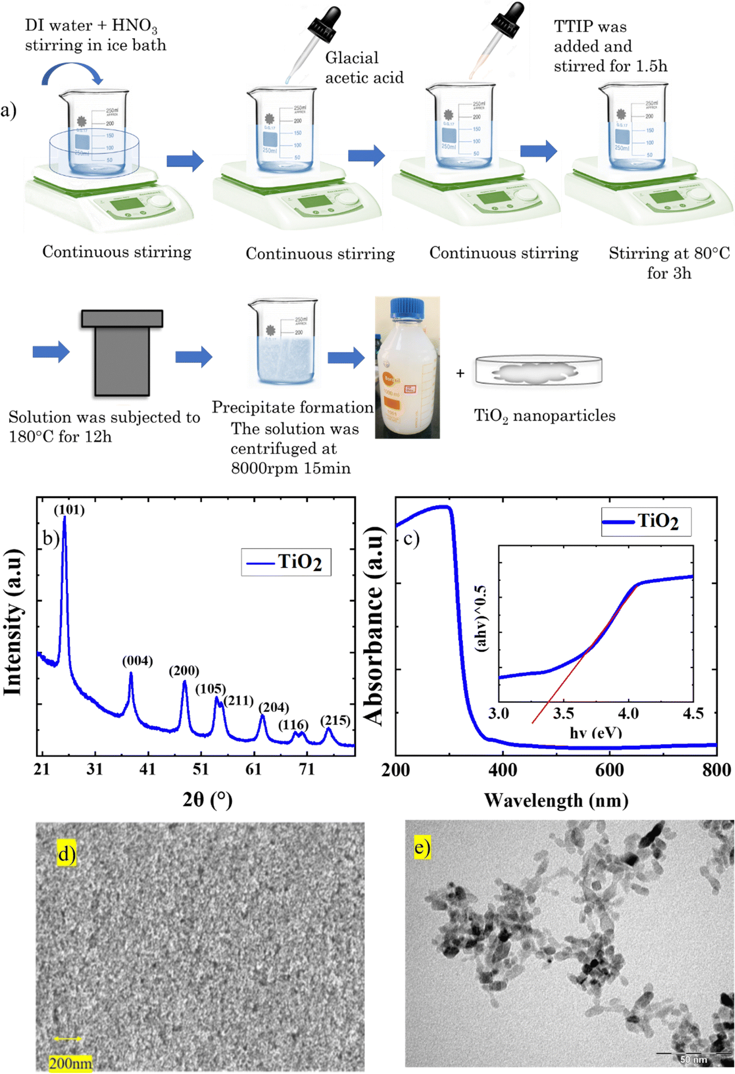 | ||
| Fig. 1 (a) Schematic representation of uniformly dispersed anatase TiO2 sol and nanoparticle synthesis, (b) XRD spectra, (c) absorbance spectra (d) FE-SEM images and (e) TEM of TiO2 films fabricated from TiO2 sol. | ||
TiO2 nanoparticles are instantaneously formed on the addition of TTIP due to the hydrolysis of the precursors in the presence of HNO3.16 The rapid nucleation leads to the formation of stabilized TiO2 nanoparticles. Subsequent aging at 80 °C triggers the formation of amorphous anatase TiO2 particles within the stabilized nuclei.16 The hydrothermal process utilizes high temperature (180 °C) and pressure aiding the formation of highly crystalline anatase TiO2 nanoparticles.
The stability of the sol was analysed by measuring the zeta potential of the dispersion. The sol exhibited a zeta potential value of 49.9 mV, which is greater than 30 mV, and hence the particles are highly dispersed in the solution medium. This suggests that the sol is a highly stable, homogeneous dispersion of TiO2 nanoparticles that can prevent the settling down of TiO2 particles for an extended period.
Crystallographic studies of the TiO2 film derived from the TiO2 sol were carried out using XRD. The XRD spectrum (Fig. 1(b)) consists of major diffraction peaks at 25.5°, 37.7°, and 48.5°, which are in agreement with the anatase phase (JCPDS 02-0406).20 The films formed are devoid of secondary phases and are highly crystalline in nature. The average crystallite size was calculated as 16.3 nm using the Scherrer equation. Fig. 1(c) represents the absorption spectra with Tauc's plot as an inset image and the yielded bandgap of 3.4 eV.
To gain further insight into the morphology and crystallographic features of the synthesized TiO2 sol, FESEM, and TEM analysis were carried out. Fig. 1(d) shows the surface morphology image of the TiO2 thin film. The films exhibit a uniformly distributed porous morphology. Fig. 1(e) represents the TEM image, which depicts the elongated TiO2 nanoparticles. As shown in Fig. S1(a) (ESI†), the sharp concentric circles from the SAED pattern were used to re-confirm the crystalline nature of the TiO2. The concentric circles of the diffraction from each plane are indexed with respect to the XRD spectra. Hence we can conclude that the highly crystalline anatase TiO2 mesoporous layer was derived from the TiO2 sol cured under ambient conditions.
Temperature dependence of TiO2 films
To evaluate the effect of temperature on the TiO2 films developed from the sol, the films were subjected to various annealing temperatures from 50 °C to 100 °C and 500 °C for 30 min, hereafter denoted as 50 TiO2, 100 TiO2, and 500 TiO2. Fig. 2(a) shows the XRD spectra of TiO2 annealed at various temperatures. The crystallinity of the films processed at 50 °C is in accordance with that of the 500 °C processed films; no significant change was observed from the XRD spectra. The absorbance (Fig. 2(b)) and transmission spectra (Fig. 2(b) inset image) also reveal identical properties for various annealing temperatures. It can be concluded that there is no notable change in the optical and crystallographic properties with a change in the temperature.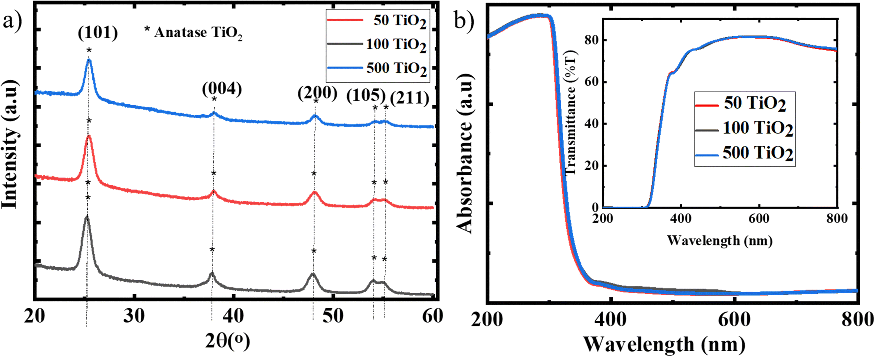 | ||
| Fig. 2 (a) XRD spectra and (b) absorption spectra with transmission spectra of 50 TiO2, 100 TiO2 and 500 TiO2 as the inset image. | ||
The variation in electrical properties with change in temperature, the direct current (DC) conductivity of the TiO2 films sintered at various temperatures were analysed by studying the current–voltage characteristics of FTO/TiO2/Au devices as shown in Fig. S2(a)–(c) (ESI†). The conductivities (σ0) were measured using the formula I = σ0Ad−1V, where A is the active area (0.12 cm2) and d (150 nm) is the thickness of the film.21 The conductivity was measured from the ohmic contact region of the IV spectra plotted in log–log scale as the TiO2 is a semiconductor material. 50 TiO2 exhibited a conductivity of 1.6 × 10⁻⁴ s cm−1, 100 TiO2-1.8 × 10⁻⁴ s cm−1 and 500 TiO2-1.6 × 10⁻⁴ s cm−1. The conductivity values of the film exhibited only a minor change. To further verify the quality of the TiO2 thin films, the trap density was calculated using the space charge limited current (SCLC) method (FTO/TiO2/PCBM/Ag) (Fig. S2(d)–(f), ESI†). The trap state density was found to increase with an increase in temperature; the values increased from 6.37 × 1017 cm−3 for 50 TiO2 to 6.97 × 1017 cm−3 for 100 TiO2 and 7.12 × 1017 cm−3 for 500 TiO2.
The effect of temperature on the surface properties of the TiO2 films was analysed by evaluating the surface roughness of the films with the help of a contact profilometer. 50 TiO2 exhibited an average roughness of 30.0 nm, 100 TiO2 35.1 nm and 500 TiO2 117 nm. The roughness of the 500 TiO2 films was very high compared to the 50 and 100 TiO2. The surface roughness of the ETL films is one of the critical factors determining the quality of the perovskite film that grows on it. To evaluate the effect of roughness on perovskite film growth, the surface morphology images of 50, 100 and 500 TiO2 before (Fig. 3(a)–(c)) and after perovskite film deposition (Fig. 3(d)–(f)) were recorded. It can be observed that the perovskite films formed on 50 TiO2 are free of pinholes and consist of well-interconnected perovskite grains. The perovskite films grown on 100 TiO2 consist of pinholes, whereas those grown on 500 TiO2 films show dendrite-like structures with many pinholes. Fig. 3(g)–(i) shows the cross section of perovskite films grown on TiO2 films. Dense MaPbI3 films were grown on 50 TiO2. Likewise, the perovskite film on 100 TiO2 is also dense, but the surface morphology shows pin holes. The MaPbI3 film grown on 500 TiO2 consists of large pin holes, which is quite evident from the cross-section and the surface image. Hence, it can be concluded that TiO2 films with lower roughness aid the growth of high-quality perovskite films.
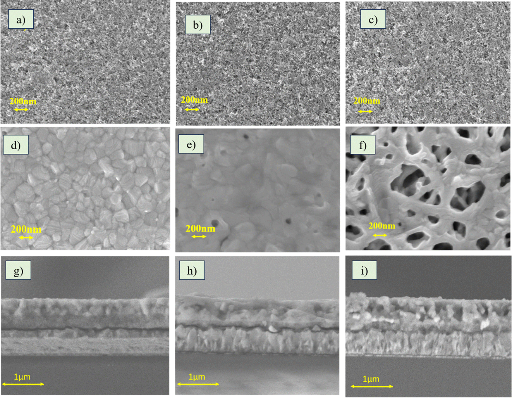 | ||
| Fig. 3 FE-SEM surface morphology images of (a) 50 TiO2, (b) 100 TiO2, (c) 500 TiO2, (d) MaPbI3 film on 50 TiO2, (e) MaPbI3 film on 100 TiO2 and (f) MaPbI3 film on 500 TiO2, and cross section image of MaPbI3 film on (g) 50 TiO2, (h) 100 TiO2 and (i) 500 TiO2. | ||
To ascertain the quality of the perovskite films formed on the TiO2 sintered at various temperatures, SCLC was carried out by constructing an electron only device (TiO2/MaPbI3/PCBM/Ag). The trap densities and the electron mobility of the perovskite deposited on 50, 100, and 500 TiO2 were calculated from the IV graphs (Fig. 4(a)–(c)), and Fig. 4(d) gives the schematic representation of the electron only devices fabricated for the analysis. Lower trap-filled limit voltage (VTFL) is obtained for 50 TiO2, indicating that the defect density has been cut down with respect to 100 and 500 TiO2.22 MAPbI3 deposited on 50 TiO2 exhibited a trap state density of 9.88 × 1017 cm−3 and mobility of 0.0124 cm2 V−1 S−1 100 TiO2 exhibited trap state density of 2.01 × 1018 cm−3 and mobility of 0.0108 cm2 V−1 S−1, and 500 TiO2 exhibited a trap density of 4.08 × 1018 cm−3 with a mobility of 4.66 × 10⁻³ cm2 V−1 S−1. Hence, we can conclude that the perovskite films formed on 500 TiO2 consisted of higher trap states and possess a lower electron mobility when compared to 50 and 100 TiO2.
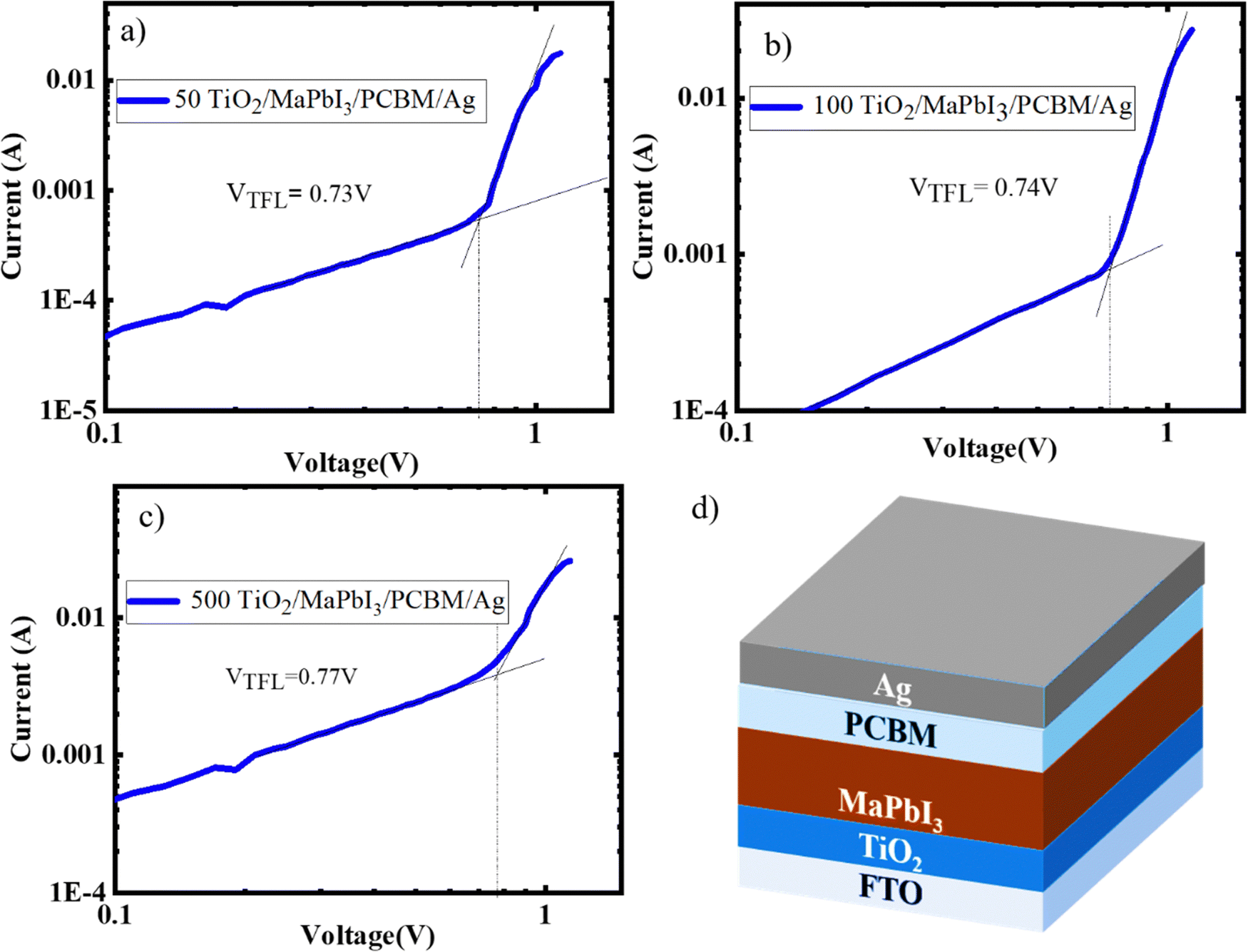 | ||
| Fig. 4 Trap density and electron mobility calculations from IV spectra using the SCLC method for MaPbI3 deposited on (a) 50 TiO2, (b)100 TiO2 and (c) 500. (d) Schematic diagram of the electron only device with device architecture TiO2/MaPbI3/PCBM/C. | ||
To probe the underlying reasons for the poor quality perovskite films grown on 500 TiO2, the surface energy of the TiO2 films was studied using the contact angle measurement (Fig. 5(a)–(c)). The high surface energy of the TiO2 surface is preferable for the wetting of the perovskite precursor.21 At the solvent–substrate interface, three forces are exerted by the surface tensions at three interfaces: liquid–surface (ls), liquid–vapour (lv), and solid–vapour (sv). At equilibrium, the forces are balanced and can be written as γsv = γls + γlv![[thin space (1/6-em)]](https://www.rsc.org/images/entities/char_2009.gif) cosθ, where cosθ gives the x-component of the liquid–vapour surface tension. Hence,
cosθ, where cosθ gives the x-component of the liquid–vapour surface tension. Hence,  can be written. If γsv > γls, cosθ is positive, and θ is <90°, which suggests that the surface is of high energy. At smaller contact angle values of the film, the surface energy of the films is higher rendering a lower critical free energy for nucleation of perovskite on the TiO2 films.
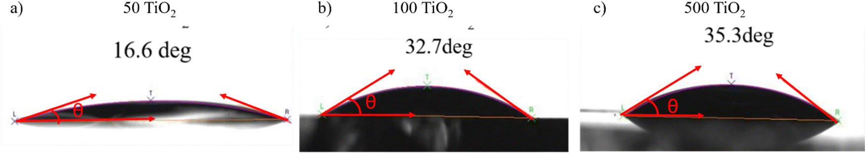 | ||
| Fig. 5 Contact angle measurements of (a) 50 TiO2, (b) 100 TiO2, and (c) 500 TiO2. | ||
The contact angle measurements help in determining the hydrophobicity/hydrophilicity of the TiO2 surface. A hydrophilic surface ensures a highly wettable surface, ensuring complete coverage of the perovskite film on the TiO2.21 The interface between the electrode and the precursor facilitates heterogeneous nucleation, which is governed by the contact angle. 50, 100 and 500 °C films exhibit hydrophilicity, with 50 °C having the highest surface energy,21 which can be co-related with the high-quality perovskite films formed on 50 TiO2.
Subsequently, the surface chemistry of the TiO2 films processed at various temperatures was analyzed using XPS to probe the variation in Ti valence states as a function of change in processing temperature. Fig. 6(a)–(c) represents the Ti2p spectra and Fig. 6(d)–(f) represents the O1s spectra of 50 TiO2, 100 TiO2, and 500 TiO2. 50 TiO2 exhibits a doublet peak at 458 eV and 463.8 eV corresponding to Ti2p3/2 and Ti2p1/2, which can be ascribed to Ti4+ in the TiO2 crystal lattice, along with a shoulder peak at 460.2 eV, which can be ascribed to Ti2p3/2, which corresponds to Ti3+ in the crystal lattice indicating the oxygen vacancies.23 Similar peaks were observed in 100 TiO2 and 500 TiO2 with slight displacement in the doublet peak towards the lower energy side of the spectra. The relative area of the Ti3+ [Ti3+/(Ti3+ + Ti4+)] peaks was calculated for 50 TiO2, 100 TiO2 and 500 TiO2, and it was observed that the lowest values were attained for 50 TiO2, indicating reduced oxygen vacancy defects in 50 TiO2 with respect to the other TiO2 electrodes under discussion.23 The same interpretation was applied to the O1s spectra, where the spectra were deconvoluted into three distinctive peaks where they can be ascribed to O–Ti4+ and the oxygen-deficient O–Ti3+ corresponding to 529.1 eV and 531.1 eV, respectively, while the –OH groups attached to TiO2 were present at 532.6 eV. A slight shift in the peaks towards high energy was observed with a change in the sintering temperatures. Notably, the relative density of –OH groups present at 50 TiO2 is higher than 100 TiO2 and 500 TiO2. The presence of –OH groups on the surface facilitates better interaction with the polar perovskite precursor, aiding improved wettability compared to 100 TiO2 and 500 TiO2. Also, the lower oxygen vacancies facilitate better conductivity, which is in accordance with the conductivity measurement data.
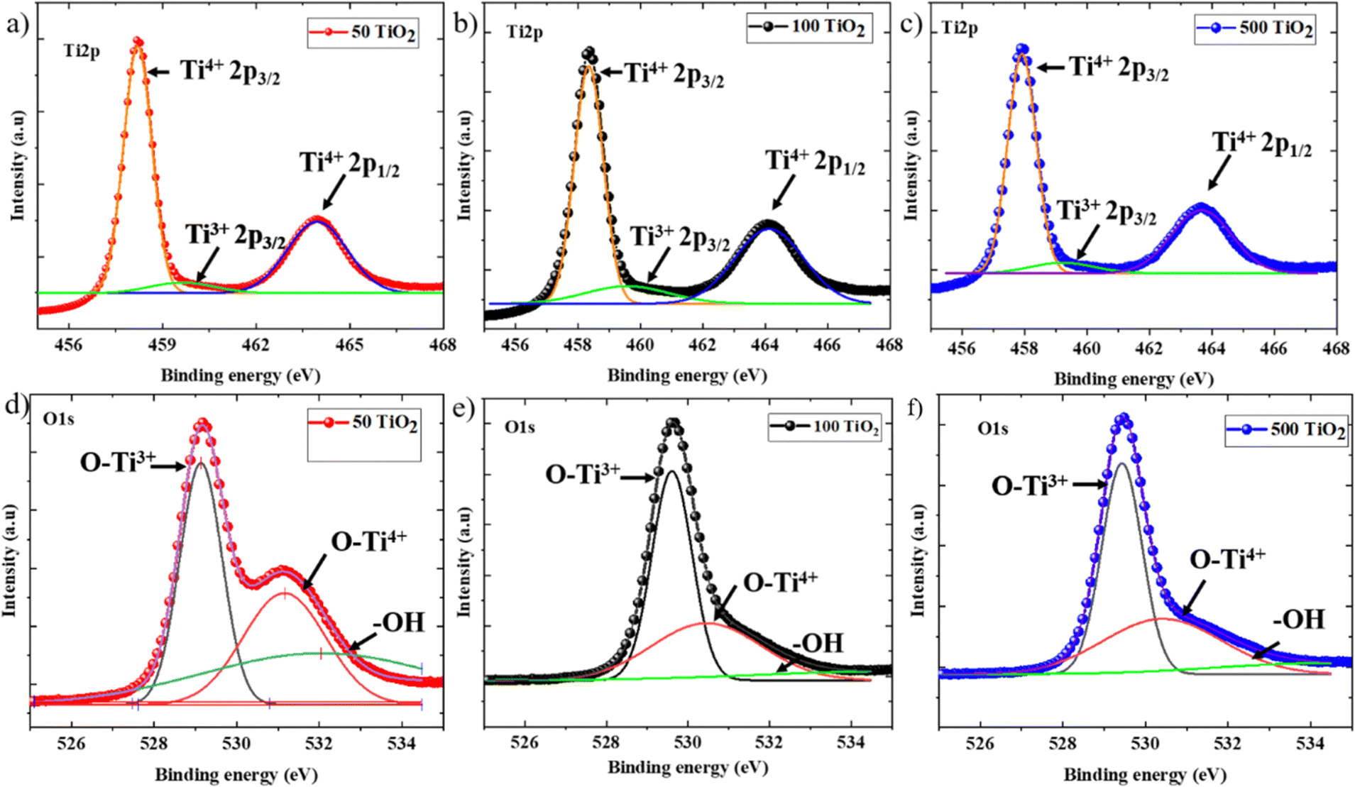 | ||
| Fig. 6 (a)–(c) Ti2p XPS spectra and (d)–(f) O1s XPS spectra of 50 TiO2, 100 TiO2 and 500 TiO2. | ||
CPSC performance
CPSCs were fabricated with various TiO2 sintering conditions. Fig. 7(a) shows the IV characteristics of the devices with the solar cell parameters tabulated in Table 1. 50 TiO2 exhibited the highest performance of 11.1% with a current density of 22.5 mA cm−2 and VOC of 0.98 V. The current density of other ETLs was found to decrease with an increase in the TiO2 sintering temperature. This decrement can be attributed to the poor coverage of the perovskite film due to the reduced surface energy of the TiO2 films. The series resistance of the devices increases with the sintering temperature of TiO2, which can be directly correlated with the changes occurring at the TiO2 electrode surface, as discussed in the above sections. Pinholes in the perovskite films, which can be observed from the FESEM images, can lead to considerable series resistance between the perovskite and carbon layer.24 50 TiO2 exhibited a higher fill factor and a lower series resistance due to the compact perovskite layer formed on the TiO2 and has a robust interface with the carbon layer, which can be observed from the CPSC device cross section image (Fig. S3, ESI†), facilitating efficient charge extraction. This clearly indicates that the entire solar cell performance is highly influenced by the properties of the ETL on which the perovskite absorber layer is coated. | ||
| Fig. 7 (a) IV characteristics of CPSCs with 50 TiO2, 100 TiO2 and 500 sintered TiO2 as the ETL; (b) PL spectra and (c) TRPL spectra of MaPbI3 films deposited on 50 TiO2, 100 TiO2 and 500 sintered TiO2. (d) Mott–Schottky analysis at 1 kHz for the TiO2/MaPbI3 carbon heterojunction solar cell. | ||
| Device id | V OC (V) | J SC (mA cm−2) | FF (%) | η (%) |
|---|---|---|---|---|
| 50 TiO2/MaPbI3/C | 0.98 | 22.3 | 49.0 | 11.1 |
| 100 TiO2/MaPbI3/C | 0.95 | 21.5 | 38.3 | 8.2 |
| 500 TiO2/MaPbI3/C | 0.95 | 19.2 | 39.0 | 7.5 |
The charge extraction properties were analysed with the aid of photoluminescence spectroscopy (PL) (Fig. 7(b)) and time resolved photoluminescence spectroscopy (TRPL) (Fig. 7(c)). MaPbI3 films deposited on 50, 100, and 500 TiO2 were excited at 540 nm, and the emission spectra were recorded. 50 TiO2 exhibited a high PL quenching followed by 100 TiO2 and 500 TiO2, indicating a fast charge extraction at the TiO2/MaPbI3 interface. A bi-exponential fit was used to extract the electron lifetime from the TRPL spectra and is recorded in Table 2. τ1, the fast decay component, is attributed to the injection of free carriers in the perovskite layer to the charge collection material, while τ2 indicated the recombination of the free carriers in the radiative channel.25 50 TiO2/MaPbI3 exhibits a faster decay (τ1) when compared to MaPbI3 on 100 and 500 TiO2. A lower τ2 value was recorded for 50 TiO2/MaPbI3, indicating lower recombination resulting in less VOC losses.
| Film | τ 1 (ns) | τ 2 (ns) | χ 2 |
|---|---|---|---|
| 50 TiO2/MaPbI3 | 5.43 | 18.7 | 1.08 |
| 100 TiO2/MaPbI3 | 6.16 | 56.3 | 1.09 |
| 500 TiO2/MaPbI3 | 5.6 | 41.0 | 1.01 |
To further understand the operation mechanism of the CPSCs with TiO2 sintered at various temperatures, capacitance–voltage measurement was carried out on TiO2/MaPbI3 heterojunction solar cells. The built-in potential was calculated to be 1.12 V, 1.06 V, and 1.04 V, respectively, for 50 TiO2, 100 TiO2, and 500 TiO2 (Fig. 7(d)) from the interception of the linear regime with the x-axis of the Mott–Schottky plot in Fig. 7(d), which helps to suppress the back reaction of electrons from the TiO2 film to the MaPbI3 film efficiently.26 50 TiO2 devices exhibited a larger built-in potential indicating a higher depletion width at the TiO2/MaPbI3 interface, successfully inhibiting the back reaction of electrons and preventing recombination, yielding a high functioning device compared to the 100 TiO2 and 500 TiO2.26 The thickness of various layers of the devices was analysed from the device cross-sectional images of the CPSCs given in Fig. S3 (ESI†).
To validate the superiority of the low temperature curable TiO2 sol, 50 TiO2 was compared with high temperature sintered commercial TiO2 (Fig. S4 and Table S1, ESI†). The device fabrication uses a simplified fabrication process with fewer fabrication steps with a single high temperature process compared to the general CPSC fabrication. The devices exhibited an enhancement in power conversion efficiency compared to the commercial TiO2 with an improved open circuit voltage and fill factor due to better TiO2 surface properties when compared to the commercial TiO2 surface.
Conclusion
A low temperature curable TiO2 sol, compatible with various coating techniques was used as the ETL in the separator and HTM-free CPSCs and was found to give an efficiency of 11% which was greater than the devices with commercial TiO2 as the ETL. The temperature dependence and changes in electrical, crystallographic, optical, and morphological properties were analysed. It was observed that the quality of the perovskite films is highly dependent on the surface energy and roughness of the TiO2 layer on which it is coated. Further optimization of the device architecture can yield a high performing device with a lower energy payback period. Since the sol can be generated in larger quantities, is compatible with various coating techniques, and can be processed at temperatures as low as ambient temperature, it can be used for flexible solar cell applications and also large-scale deposition techniques.Conflicts of interest
There are no conflicts to declare.Acknowledgements
The authors acknowledge the Department of Science and Technology, New Delhi, India, for the financial support through SERB Research Scientist (SB/SRS/2019-20/22PS), and TRC (AI/1/65/ARCI/2014).References
- H. S. Jung and N. G. Park, Perovskite solar cells: From materials to devices, Small, 2015, 11(1) DOI:10.1002/smll.201402767.
- A. Kojima, K. Teshima, Y. Shirai and T. Miyasaka, Organometal halide perovskites as visible-light sensitizers for photovoltaic cells, J. Am. Chem. Soc., 2009, 131(17), 6050–6051, DOI:10.1021/ja809598r.
- P. Roy, N. Kumar Sinha, S. Tiwari and A. Khare, A review on perovskite solar cells: Evolution of architecture, fabrication techniques, commercialization issues and status, Sol. Energy, 2020, 198, 665–688, DOI:10.1016/j.solener.2020.01.080.
- Z. Ku, Y. Rong, M. Xu, T. Liu and H. Han, Full printable processed mesoscopic CH3NH3PbI3/TiO2 heterojunction solar cells with carbon counter electrode, Sci. Rep., 2013, 3, 3132, DOI:10.1038/srep03132.
- T. Liu, L. Liu, M. Hu, Y. Yang, L. Zhang, A. Mei and H. Han, Critical parameters in TiO2/ZrO2/Carbon-based mesoscopic perovskite solar cell, J. Power Sources, 2015, 293, 533–538, DOI:10.1016/j.jpowsour.2015.05.106.
- M. Shahiduzzaman, S. Visal, M. Kuniyoshi, T. Kaneko, S. Umezu, T. Katsumata, S. Iwamori, M. Kakihana, T. Taima, M. Isomura and K. Tomita, Low-Temperature-Processed Brookite-Based TiO2 Heterophase Junction Enhances Performance of Planar Perovskite Solar Cells, Nano Lett., 2019, 19, 598–604, DOI:10.1021/acs.nanolett.8b04744.
- Z. Cao, C. Li, X. Deng, S. Wang, Y. Yuan, Y. Chen, Z. Wang, Y. Liu, L. Ding and F. Hao, Metal oxide alternatives for efficient electron transport in perovskite solar cells: Beyond TiO2 and SnO2, J. Mater. Chem. A, 2020, 8, 19768–19787, 10.1039/d0ta07282f.
- H. Zhou, Y. Shi, K. Wang, Q. Dong, X. Bai, Y. Xing, Y. Du and T. Ma, Low-temperature processed and carbon-based ZnO/CH3NH3PbI3/C planar heterojunction perovskite solar cells, J. Phys. Chem. C, 2015, 119, 4600–4605, DOI:10.1021/jp512101d.
- F. Deng, X. Sun, X. Lv, Y. Li, S. Li, Y. Z. Zheng and X. Tao, All room-temperature processing efficient planar carbon-based perovskite solar cells, J. Power Sources, 2021, 489, 229345, DOI:10.1016/j.jpowsour.2020.229345.
- J. P. Correa Baena, L. Steier, W. Tress, M. Saliba, S. Neutzner, T. Matsui, F. Giordano, T. J. Jacobsson, A. R. Srimath Kandada, S. M. Zakeeruddin, A. Petrozza, A. Abate, M. K. Nazeeruddin, M. Grätzel and A. Hagfeldt, Highly efficient planar perovskite solar cells through band alignment engineering, Energy Environ. Sci., 2015, 8, 2928–2934, 10.1039/c5ee02608c.
- Y. Li, J. K. Cooper, W. Liu, C. M. Sutter-Fella, M. Amani, J. W. Beeman, A. Javey, J. W. Ager, Y. Liu, F. M. Toma and I. D. Sharp, Defective TiO2 with high photoconductive gain for efficient and stable planar heterojunction perovskite solar cells, Nat. Commun., 2016, 7, 1–7, DOI:10.1038/ncomms12446.
- D. Yang, R. Yang, J. Zhang, Z. Yang, S. Liu and C. Li, High efficiency flexible perovskite solar cells using superior low temperature TiO2, Energy Environ. Sci., 2015, 8, 3208–3214, 10.1039/c5ee02155c.
- P. S. C. Schulze, A. J. Bett, K. Winkler, A. Hinsch, S. Lee, S. Mastroianni, L. E. Mundt, M. Mundus, U. Würfel, S. W. Glunz, M. Hermle and J. C. Goldschmidt, Novel Low-Temperature Process for Perovskite Solar Cells with a Mesoporous TiO2 Scaffold, ACS Appl. Mater. Interfaces, 2017, 9, 30567–30574, DOI:10.1021/acsami.7b05718.
- B. Conings, L. Baeten, T. Jacobs, R. Dera, J. D’Haen, J. Manca and H. G. Boyen, An easy-to-fabricate low-temperature TiO2 electron collection layer for high efficiency planar heterojunction perovskite solar cells, APL Mater., 2014, 2(8), 081505–081508, DOI:10.1063/1.4890245.
- D. Li, Y. Chen, P. Du, Z. Zhao, H. Zhao, Y. Ma and Z. Sun, An annealing-free anatase TiO2 nanocrystal film as an electron collection layer in organic solar cells, RSC Adv., 2015, 5, 88973–88978, 10.1039/c5ra16932a.
- C. Yang, M. Yu, D. Chen, Y. Zhou, W. Wang, Y. Li, T. C. Lee and D. Yun, An annealing-free aqueous-processed anatase TiO2 compact layer for efficient planar heterojunction perovskite solar cells, Chem. Commun., 2017, 53, 10882–10885, 10.1039/c7cc01104k.
- M. Guo, D. Shen, Y. Li, M. A. Akram and M. Wei, TiO2 Mesocrystals Processed at Low Temperature as the Electron-Transport Material in Perovskite Solar Cells, ChemSusChem, 2020, 13, 5256–5263, DOI:10.1002/cssc.202001486.
- B. Ding, S. Y. Huang, Q. Q. Chu, Y. Li, C. X. Li, C. J. Li and G. J. Yang, Low-temperature SnO2-modified TiO2 yields record efficiency for normal planar perovskite solar modules, J. Mater. Chem. A, 2018, 6, 10233–10242, 10.1039/c8ta01192c.
- T. Shi, S. Lin, M. Fang, D. Kong, Y. Yuan, Y. Gao, B. Yang, H. Han and C. Zhou, Low-temperature fabrication of carbon-electrode based, hole-conductor-free and mesoscopic perovskite solar cells with power conversion efficiency >12% and storage-stability >220 days, Appl. Phys. Lett., 2020, 117, 163501, DOI:10.1063/5.0025442.
- Y. Yang, K. Ri, A. Mei, L. Liu, M. Hu, T. Liu, X. Li and H. Han, The size effect of TiO2 nanoparticles on a printable mesoscopic perovskite solar cell, J. Mater. Chem. A, 2015, 3, 9103–9107, 10.1039/c4ta07030e.
- M. S. You, J. H. Heo, J. K. Park, S. H. Moon, B. J. Park and S. H. Im, Low temperature solution processable TiO2 nano-sol for electron transporting layer of flexible perovskite solar cells, Sol. Energy Mater. Sol. Cells, 2019, 194, 1–6, DOI:10.1016/j.solmat.2019.02.003.
- G. Liu, B. Yang, H. Chen, Y. Zhao, H. Xie, Y. Yuan, Y. Gao and C. Zhou, In situ surface modification of TiO2 by CaTiO3 to improve the UV stability and power conversion efficiency of perovskite solar cells, Appl. Phys. Lett., 2019, 115, 213501, DOI:10.1063/1.5131300.
- S. Ranjan, R. Ranjan, A. Tyagi, K. S. Rana, A. Soni, H. K. Kodali, V. Dalal, A. Singh, A. Garg, K. S. Nalwa and R. K. Gupta, Low-Temperature Microwave Processed TiO2 as an Electron Transport Layer for Enhanced Performance and Atmospheric Stability in Planar Perovskite Solar Cells, ACS Appl. Energy Mater., 2022, 5, 2679–2696, DOI:10.1021/acsaem.1c02675.
- A. Bahtiar, S. Rahmanita and Y. D. Inayatie, Pin-Hole Free Perovskite Film for Solar Cells Application Prepared by Controlled Two-Step Spin-Coating Method, IOP Conf. Ser.: Mater. Sci. Eng., 2017, 196, 012037, DOI:10.1088/1757-899X/196/1/012037.
- J. Yin, J. Cao, X. He, S. Yuan, S. Sun, J. Li, N. Zheng and L. Lin, Improved stability of perovskite solar cells in ambient air by controlling the mesoporous layer, J. Mater. Chem. A, 2015, 3, 16860–16866, 10.1039/c5ta02843d.
- F. Zhang, X. Yang, H. Wang, M. Cheng, J. Zhao and L. Sun, Structure engineering of hole-conductor free perovskite-based solar cells with low-temperature-processed commercial carbon paste as cathode, ACS Appl. Mater. Interfaces, 2014, 6, 16140–16146, DOI:10.1021/am504175x.
Footnote |
| † Electronic supplementary information (ESI) available. See DOI: https://doi.org/10.1039/d3ma00427a |
| This journal is © The Royal Society of Chemistry 2024 |