
 Open Access Article
 This Open Access Article is licensed under a
 Creative Commons Attribution 3.0 Unported Licence
Perovskite-inspired Cu2AgBiI6 for mesoscopic indoor photovoltaics under realistic low-light intensity conditions†
G. Krishnamurthy
Grandhi
a,
Sami
Toikkonen
a,
Basheer
Al-Anesi
 a,
Vincenzo
Pecunia
b and
Paola
Vivo
*a
a,
Vincenzo
Pecunia
b and
Paola
Vivo
*a
aHybrid Solar Cells, Faculty of Engineering and Natural Sciences, Tampere University, P.O. Box 541, FI-33014 Tampere University, Finland. E-mail: paola.vivo@tuni.fi
bSchool of Sustainable Energy Engineering, Simon Fraser University, 5118 – 10285 University Drive, Surrey, V3T 0N1, BC, Canada
First published on 9th November 2022
Abstract
The considerable potential of perovskite-inspired Cu2AgBiI6 (CABI) photovoltaics under both solar and artificial lighting has been recently highlighted. However, to realistically ensure the suitability of CABI-based indoor photovoltaics (IPVs) to power the Internet of Things (IoT) ecosystem, it is necessary to study how the device performance is affected by very low-light intensity conditions (200–50 lux illumination). In this work, we find that the fine-tuning of the mesoporous TiO2 (mp-TiO2) layer thickness is crucial to maximize the performance of mesoporous CABI-based IPVs at both high and very-low artificial light intensity as it directly affects the charge extraction and non-radiative charge recombination in the devices. An optimal mp-TiO2 thickness of ∼200 nm leads to an indoor power conversion efficiency (PCE(i)) of 5.52% and a fill factor of 69%, which are the highest values for perovskite-inspired based IPVs under 1000 lux white light-emitting diode lighting. Importantly, the devices keep a high fill factor also at very low-light intensity. This guarantees a noteworthy PCE(i) value of 4.64% at 200 lux and an open-circuit voltage (VOC) of 0.38 V even at 50 lux. Our work suggests that, upon further improvements in the short-circuit current and VOC values, low-toxicity mesoscopic CABI-based IPVs may approach their theoretical PCE(i) values of 50–60% even under very low-light intensity conditions.
Introduction
The demand for self-powered wireless sensors for the Internet of things (IoT) has been exponentially increasing over the last few years.1–3 Many of these devices are installed or used indoors, which make them particularly attractive to harvest artificial lighting via indoor photovoltaics (IPVs) for being sustainably powered.3–5 Given the limited power density emitted by common indoor light sources (in tens to a few hundred μW cm−2, i.e., orders of magnitude lower than outdoor terrestrial sunlight), it is crucial to develop IPVs that can efficiently function under such low-light conditions to be able to reliably power IoT devices. Moreover, typical artificial light sources, such as white light-emitting diodes (WLEDs), emit solely in the visible range, leading to the need for photovoltaic absorbers with a bandgap in the range of 1.9–2.0 eV for maximum IPV efficiency.4,6 Among emerging IPV light-harvesters, lead halide perovskites (LHPs) are advantageous because of their low-cost, solution processability, and favourable optoelectronic properties, which have recently led to the highest ever indoor power conversion efficiency (PCE(i)) of 40.1%.7 However, the lead in LHP devices raises toxicity concerns, which overshadow their impressive performance.8,9 Lead release from IPVs embedded within IoT devices represents a significant health risk since the devices are close to the human end-user, unlike the case of solar cells installed on rooftops or in solar farms. This calls for the design and development of IPVs based on lead-free halide perovskites and perovskite-inspired materials (PIMs).3,10 Amongst this broad family of lead-free compounds,3,11,12 pnictohalide-based embodiments (i.e., compounds comprising Bi or Sb alongside halide anions) are typically air-stable due to the inherent stability of the pnictogen 3+ cations.13–16 This property represents an added value for practical applications compared to the popular tin (Sn)-based halide perovskites, which, by contrast, suffer from the rapid oxidation of Sn2+.17 Furthermore, the bandgaps of pnictohalide-based PIMs often lie in the range of the optimum bandgap (1.9–2.0 eV) for IPVs, which could ultimately lead to a PCE(i) up to ≅60% in the radiative limit.3,10 Yet, the field is in its early infancy and only a few pnictohalides-based PIMs have been investigated for use in IPVs, such as antimony (Sb)-based PIMs and silver iodobismuthates.5,10,18 Notably, the IPV efficiencies of pnictohalides-based PIMs reported to date have been up to 5%,5,10,18 which is already in the range of mainstream commercial IPV based on amorphous silicon. Given the considerably higher maximum efficiency, these results prompt the investigation of materials and device engineering strategies to bridge the gap to their ultimate theoretical IPV efficiencies.For any IPV technology to serve the purpose of powering IoT sensor nodes, it is crucial to ensure that it functions efficiently under real-world conditions. Defining realistic indoor lighting conditions for IPV characterization is not trivial as indoor illumination may be direct or diffuse. Thomas et al. estimated that an IoT device could be illuminated by indoor light levels down to 100–150 lux.19 Importantly, reports on PIMs-based IPVs to date, as well as a wide number of other emerging IPV technologies, typically refer to their characterization at 1000 lux, thereby preventing a complete assessment of their realistic potential for powering IoT devices.
Cu2AgBiI6 (CABI) is a newly proposed PIM with favorable optoelectronic properties that has rapidly received great interest from the solar cell community.18,20–25 Very recently, we successfully improved the film morphology and increased the surface coverage of CABI films.18 As a result of the reduced interfacial recombination, we achieved IPVs with a promising PCE(i) of 4.7% under 1000 lux WLED illumination, which is already approaching that of commercially available a-Si:H IPVs.18 Nevertheless, the potential of CABI under very low illuminance, i.e., lower than 1000 lux, has not yet been evaluated.
Mesoscopic architectures of PIM-based devices have enabled superior charge extraction, in turn leading to the highest power conversion efficiencies compared to their planar counterparts.25–29 Herein, we investigate IPVs with mesoscopic architecture containing a CABI light-harvesting layer. We find that the thickness optimization of the mp-TiO2 layer is critical to maximize the PCE (1.26%) of hysteresis-free mesoscopic CABI solar cells under 1-sun illumination and the PCE(i) (5.52%) under 1000 lux, which is the highest reported to date for PIM-based IPVs. Importantly, we show that the introduction of a mp-TiO2 layer with an optimal thickness, by significantly reducing the shunt pathways, results in an unchanged fill factor (FF) also under very low-light intensity conditions (50–200 lux). Our study suggests that identifying ad hoc processing protocols and device architectures is paramount to fully exploit the potential of new PIMs under realistic low-light intensity conditions.
Results and discussion
CABI thin films were first deposited on c-TiO2 and mp-TiO2 surfaces in an inert environment and then heated in air by following an established two-step annealing process at 50 and 200 °C.18,20 The X-ray diffraction (XRD) patterns of the films (Fig. 1a) indicate the formation of CABI as the dominant phase, along with a small fraction of an impurity phase, in agreement with earlier findings.20 Detailed information on the crystal structure of CABI can be found in the first study by Sansom et al. on this layered material.20 Scanning electron microscopy-energy dispersive X-ray spectroscopy (SEM-EDS) analysis shows that CABI films on FTO|c-TiO2 and FTO|c-TiO2|mp-TiO2 substrates have average bulk compositions of Cu1.9AgBi0.7I4 and Cu2AgBi0.7I4, respectively. The lower bismuth and iodine compositional values can be partially attributed to the presence of Cu2BiI5 impurities (Fig. 1a) and the possible evaporation of iodine under strong electron beam exposure.18 The optical absorption spectra of the CABI films show a peak related to CABI at ∼580 nm and an unassigned peak at 420 nm (Fig. S1 of the ESI†).18 The films have a direct band gap of 1.91 eV, as extracted from their absorption edges in the Tauc plots of Fig. 1b. The examination of the emission properties of the films reveals their weak and broad photoluminescence (PL) signal that peaks at 715 nm (Fig. 1c). The emission appears only when the excitation energy is above 420 nm, and its origin is still unclear, as discussed in our previous work on CABI.18 One would expect PL quenching for CABI films on TiO2 due to the electron transfer from the CABI layer to TiO2, although the PL intensity is highest for the CABI film when deposited on mp-TiO2 than on c-TiO2 or glass. The time-resolved PL (TRPL) decay curves of the three samples of Fig. 1d are fitted with a bi-exponential function and the corresponding parameters are presented in Table S1.† All the three samples exhibit a relatively long radiative lifetime of 51 to 70 ns. The contribution of radiative component (Arad (%)) is considerably higher for mp-TiO2|CABI than the other two samples (see Table S1†). Furthermore, the distribution coefficient (β) (obtained by fitting the decay curve using a stretched exponential function) value of 0.62 is also higher for the CABI film on mp-TiO2 compared to the other samples (β = 0.46 and 0.49), which indicates a reduced heterogeneity (the number of the decay channels) of the excited state decay or the enhanced radiative recombination (Table S1†). Therefore, the improved radiative recombination (or high PL intensity) may be attributed to the formation of a high-quality CABI film on the mp-TiO2 surface with a reduced number of surface defects at mp-TiO2|CABI, which dominates the PL quenching effect. | ||
Fig. 1 (a) XRD patterns of CABI films deposited on FTO|c-TiO2 and FTO|c-TiO2|mp-TiO2 along with the reference pattern of CABI (CCDC code: 2![[thin space (1/6-em)]](https://www.rsc.org/images/entities/char_2009.gif) 013668). (b) Tauc plot of the CABI films. (c) PL spectra (which were obtained by dividing the corresponding as-measured PL spectra with the absorbance values at the excitation wavelength of 405 nm) with the x-axes on both wavelength (bottom) and energy (top) units and (d) TRPL decay curves of the CABI films. SEM top view images of CABI films deposited on (e) FTO|c-TiO2 and on (f) FTO|c-TiO2|mp-TiO2. 013668). (b) Tauc plot of the CABI films. (c) PL spectra (which were obtained by dividing the corresponding as-measured PL spectra with the absorbance values at the excitation wavelength of 405 nm) with the x-axes on both wavelength (bottom) and energy (top) units and (d) TRPL decay curves of the CABI films. SEM top view images of CABI films deposited on (e) FTO|c-TiO2 and on (f) FTO|c-TiO2|mp-TiO2. | ||
SEM top-view images in Fig. 1e and f present the morphology of the CABI films. The film on the c-TiO2 layer has micron-sized CABI domains separated by gaps (large pin holes). In the case of the film deposited on mp-TiO2, most of the CABI layer is infiltrated into the mesoporous layer; however, a thin CABI layer is still present outside the mesoporous structure (Fig. 1f and S2†). This capping layer is thick enough to prevent the direct contact between the TiO2 ETL and the hole-transport layer (HTL), as shown in the SEM cross-sectional image of the FTO|c-TiO2|mp-TiO2|CABI|Spiro-OMeTAD|Au (referred to as CABI-Meso in the following) solar cell shown in Fig. 2a. The same figure also contains the cross-sectional view of the FTO|c-TiO2CABI|Spiro-OMeTAD|Au (referred to as CABI-Planar in the following) device.
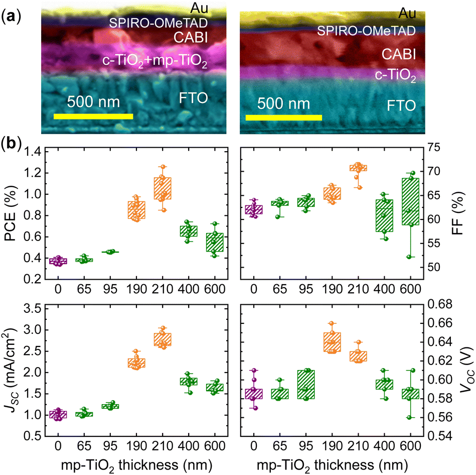 | ||
| Fig. 2 (a) Cross-sectional SEM images of CABI-Meso (left) and CABI-Planar (right) photovoltaic cells. (b) Statistical distributions of the photovoltaic parameters of CABI devices as a function of mp-TiO2 layer thickness, under 1-sun illumination. | ||
To maximize the performance of CABI-based IPV cells, we have optimized the thickness of the mp-TiO2 layer (from 0 to 600 nm) by simply controlling its precursor solution concentration in the range from 0.05 g mL−1 to 0.45 g mL−1 prior to the spin-coating of the layer. Complete details of the device fabrication can be found in the Experimental section. We first studied the device characteristics of mesoscopic CABI devices under AM 1.5 G 1-sun illumination to compare their performance with that of state-of-the-art CABI solar cells. The average power conversion efficiency (PCE) of the CABI solar cells gradually increases from 0.37% to 0.86% when the mp-TiO2 layer thickness varies from zero to 190 nm, and a further increase in the thickness value to 210 nm raises the average PCE to the highest value of 1% (Fig. 2b and Table S2†). Further increase in the thickness reduces the PCE of the devices. Therefore, 190–210 nm is the optimized thickness for the mp-TiO2 layer for the CABI devices fabricated in this work. The champion CABI-Meso device delivers a PCE of 1.26%, which is comparable with the highest PCE values reported for the CABI-planar and mesoscopic solar cells fabricated with the same metal electrode (i.e., Au).18,24,25 The FF value of 72% of the CABI-Meso device (Fig. 2b) is markedly the highest FF ever achieved for a CABI solar cell fabricated with the same metal electrode.18,20,24,25 The external quantum efficiency (EQE) values of this device are ∼29% and 18% at 370 nm and 580 nm, respectively (Fig. S3†), which are comparable to the values reported earlier for CABI.18,24 The short-circuit current density (JSC) value (from current density (J)–voltage (V) scans) of 3.0 mA cm−2 of the champion device closely matches the value extracted from its EQE spectrum (2.9 mA cm−2). While a significant hysteresis between the reverse and forward J–V scans is quite typical of pristine CABI-Planar devices,18,20,24 when adopting a mesoscopic architecture, the hysteresis is nearly suppressed (see Fig. 3a for the comparison). The minimization of J–V hysteresis by employing a mp-TiO2 layer has been already observed in the case of lead halide perovskite solar cells, and the reduction of mobile ion density or carrier trapping at the interface of the absorber layer of the device was provided as one of the plausible explanations for the hysteresis alleviation.30,31 The hysteresis of the CABI-Planar devices and the devices with a thicker or thinner mp-TiO2 layer than the optimized one gradually increases when lowering the light intensity (0.1–1.2 suns), as shown in Fig. S4.† This may be attributed to a pronounced ion migration or charge trapping effects at low-intensity illuminations.32 Yet, the best CABI-Meso devices exhibit negligible J–V hysteresis regardless of the illumination intensity.
 | ||
| Fig. 3 (a) J–V curves (reverse and forward bias scans) of the CABI-Meso and CABI-Planar champion cells. (b) Variation of the slope of VOC-suns (i.e., ideality factor) with the mp-TiO2 layer thickness. (c) Log–log plot of JSCversus 1-sun intensity for the devices. (d) FF variation with 1-sun intensity. | ||
More than two-fold improvement in the PCE of the CABI-Meso devices compared to that of their CABI-Planar counterparts is due to the increase in all three photovoltaic parameters (FF, JSC, and, open-circuit voltage (VOC)). The slope (in a semi-log plot) of VOC trend as a function of light intensity (0.1 to 1.2 suns) is equal to nIDkBT/q, where nID is the ideality factor (and kB, T and q are Boltzmann's constant, temperature, and elementary charge, respectively). The lower nID values (∼1.0) of the high-performing CABI-Meso device compared to the CABI-Planar device (nID = 1.6) or devices with a thinner mp-TiO2 layer suggests a reduced trap-assisted recombination under open-circuit conditions (see Fig. 3b).33,34 This can be supported by the high PL intensity and enhanced radiative recombination of mp-TiO2|CABI (Fig. 1c and d). Furthermore, the log–log plot of JSCvs. light intensity (I) (see Fig. 3c) determines the value of the exponent, α, as JSC ∝ Iα. The value of α ≈ 1 for the CABI-Meso device indicates a fixed number of carrier trapping centers through which the recombination takes place.26 On the other hand, 0.5< α < 1 in the CABI-Planar device specifies a broad (i.e., energy-dependent) distribution of defect states within the forbidden gap (Rose–Bube's one-center model).26 In other words, the trap-assisted recombination is higher in CABI-Planar devices under short-circuit conditions. Therefore, the enhancement in JSC and VOC in the high-performing CABI-Meso devices can be attributed to a lowered non-radiative charge-carrier recombination alongside the enhanced charge extraction inherent in mesoporous architecture. The high FF of the champion devices (Fig. 2b) indicates that the mp-TiO2 layer with an optimized thickness extracts the charges efficiently, thus minimizing the charge transport losses.35 This is consistent with the near linear growth of JSC with the 1-sun intensity (Fig. 3c). The FF values are reduced for the devices with thicker mp-TiO2 layers (>210 nm). These devices have the CABI layer completely infiltrated into the mp-TiO2 layer, enabling direct contact between the mp-TiO2 layer and the HTL, as shown in Fig. S5.† This leads to additional recombination pathways, and the non-linear (or dual-slope nature) JSC trend suggests the same (see Fig. S6†). The reduced amount of CABI in contact with the HTL also increases the recombination probability and hampers the photogenerated hole extraction to the HTL. A high FF of the devices with optimized mp-TiO2 thicknesses can also be partially ascribed to lower series resistance values (20 ± 4 Ω cm2) compared to CABI-Planar devices (51 ± 14 Ω cm2). However, the resistance values in both cases are still high enough to cause a gradual loss in the FF with 1-sun light intensity (Fig. 3d).34
The stability of an unencapsulated CABI-Meso device (stored in dry air with 15% RH at 25 °C) has been monitored for more than a month as shown in Fig. S7.† During this period, the device retains 99% of its initial PCE. At the beginning, a 6% drop in the PCE value is noted due to a loss in JSC. However, the small and gradual growth of VOC and the FF afterward compensates for the initial JSC loss, in turn guaranteeing a nearly unchanged PCE value after 35 days of air storage.
The good match between the EQE spectrum of CABI solar cells and the emission spectrum of a white light-emitting diode (WLED) (Fig. S8†) hints at a higher PCE under the WLED illumination.18 The statistical distributions of photovoltaics parameters of the optimized CABI-Meso devices obtained from the J–V scans recorded under WLED (1000 lux) illumination are shown in Fig. 4a. The champion device delivers a FF = 67%, VOC = 0.53 V, JSC = 72 μA cm−2, and a corresponding hysteresis-free indoor PCE (PCE(i)) of 5.52% (see Fig. 4b), which is the highest value ever reported for PIM-based photovoltaics under the same illumination conditions (1000 lux).5,10,18 On the other hand, CABI-Planar devices achieve a maximum PCE(i) of just 2.27%, closely matching with the value obtained in a previous work.18 The integrated JSC of 66 μA cm−2 of the champion device (see Fig. 4c) obtained based on its EQE spectrum and irradiance curve of the WLED is close to the value from the J–V measurement (JJ–VSC = 72 μA cm−2), thus validating our indoor photovoltaic measurements. CABI-Meso devices delivered an average FF of 65%, with the highest FF approaching 69%. These values are higher than those of the CABI-Planar devices (Table 1).18 The high FF, the linear trend of JSC with light intensity (see Fig. 3c), and the high radiative lifetime of the absorber layer (Fig. 1d) suggest better charge extraction and transport in CABI-Meso devices, which leads to the record PCE(i) among the PIM-based IPVs. A similar positive role of the mp-TiO2 layer under indoor illumination has been demonstrated previously for LHPs.36,37
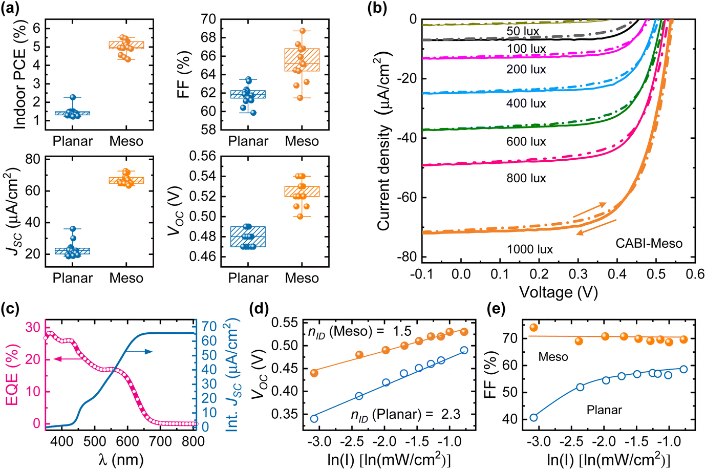 | ||
| Fig. 4 (a) The statistical distribution of the photovoltaic parameters of CABI-Meso and CABI-Planar devices under 1000 lux (WLED) illumination. (b) Reverse bias (solid curve) and forward bias (dotted curve) J–V curves (reverse bias scans) of the champion CABI-Meso device under varying WLED illumination (50 to 1000 lux). (c) EQE spectrum of the CABI-Meso device and its integrated JSC spectrum over the 4000 K WLED (1000 lux). (d) VOC-WLED light intensity trend for the CABI-Meso device. (e) FF variation with WLED light intensity for CABI-Meso and CABI-Planar devices. | ||
| Devices | PCE(i) % | FF % | J SC μA cm−2 | V OC V |
|---|---|---|---|---|
| CABI-Planar | 1.44 ± 0.23 (2.27) | 62 ± 0.9 (63) | 23 ± 4 (36) | 0.48 ± 0.01 (0.49) |
| CABI-Meso | 5.00 ± 0.36 (5.52) | 65 ± 0.9 (69) | 67 ± 3 (73) | 0.52 ± 0.01 (0.54) |
Typically, in the literature the PCE(i)s of PIM-based devices have been mostly reported under 1000 lux light illumination,5,10,18 except for the PCE(i)s of 4.75% (reverse bias scan) and 4.25% (forward bias scan) at 500 lux reported for silver iodobismuthates.5 However, the illuminance levels of typical indoor light sources lie in the 200–700 lux range.6 In this study, we have recorded the J–V curves of the champion CABI-Meso device also under very low WLED illuminations, i.e., down to 50 lux (Fig. 4b), to target realistic low-light intensity conditions of buildings.19 The device generates a PCE(i) of 4.64% under 200 lux illumination (see Table 2). Notably, VOC values of 0.48 and 0.44 V are obtained at 200 and 100 lux illuminations, respectively (see Table 2). Importantly, the VOC is 0.38 V (∼60% of its value under 1-sun) even when the illuminance is as low as 50 lux. As a result, the device can generate a reasonable power output even at 50 lux (see Table 2 and Fig. 4b). By contrast, the CABI-Planar device failed to generate any VOC or photocurrent at the illumination of 50 lux (Fig. S9†). A big drop in VOC values under such dim light conditions is usually unavoidable as the ratio between the number of charge carriers generated to the number of traps in the bulk of the material is small.38 In our case, the ideality factor value of the Meso device increases to only 1.5 (Fig. 4d) from 1.0 (Fig. 3b) even when the illumination intensities vary from very high (10 to 120 mW cm−2) to very low (0.046 to 0.46 mW cm−2). This suggests that the increase in trap-assisted recombination in CABI-Meso is small when lowering the light intensity, and thus the corresponding VOC drop is minimal. CABI IPV devices, compared to those based on other common PIMs (e.g. Sb- and Bi-based), exhibit a relatively stable trend of the VOCvs. indoor light intensity in the 100–1000 lux range.10 This is one of the requirements for effective low-light intensity harvesting.
| Light intensity | J–V scan direction | PCE(i) % | FF % | J SC μA cm−2 | V OC V |
|---|---|---|---|---|---|
| 1000 lux | Reverse | 5.52 | 67 | 72 | 0.53 |
| Forward | 5.51 | 66 | 71 | 0.54 | |
| 800 lux | Reverse | 4.73 | 69 | 49 | 0.52 |
| Forward | 4.57 | 65 | 49 | 0.53 | |
| 600 lux | Reverse | 4.71 | 69 | 37 | 0.51 |
| Forward | 4.48 | 65 | 37 | 0.52 | |
| 400 lux | Reverse | 4.66 | 71 | 25 | 0.49 |
| Forward | 4.30 | 65 | 24 | 0.50 | |
| 200 lux | Reverse | 4.64 | 69 | 13 | 0.47 |
| Forward | 4.20 | 63 | 13 | 0.48 | |
| 100 lux | Reverse | 5.07 | 74 | 7 | 0.45 |
| Forward | 3.68 | 57 | 7 | 0.44 | |
| 50 lux | Reverse | 1.50 | 49 | 2 | 0.38 |
| Forward | 1.00 | 40 | 2 | 0.34 |
A high and stable FF variation (in the 100–1000 lux range) is crucial for the IPV devices to produce comparable PCE(i) values at high (1000 lux) and low (100 to 200 lux) intensity illuminations. This is what takes place, for instance, in high-performing LHP and organic IPVs, where the difference in FF values between the high-light (1-sun or 1000 lux) and low-light intensity illuminations (200 lux) is small.39 The CABI-Meso device exhibits a stable FF trend as a function of light intensity, as shown in Fig. 4e. The shunt resistance is one of the key factors that affect the FF under low-intensity illuminations.40 The shunt resistance values are higher for the CABI-Meso devices (average = 8 ± 2 kΩ cm2; highest = 12 kΩ cm2) compared to the CABI-Planar ones (average = 5 ± 1 kΩ cm2; highest = 6 kΩ cm2). This suggests a low number of shunt paths across the CABI-Meso device that induce a minimal effect on the FF under low light conditions. On the other hand, the CABI-Planar device (Fig. 4e) and other reported PIM-based devices show a typical gradual drop in the FF when lowering the light intensity.10,18 The large pin holes observed from the SEM image of Fig. 1e can bring the ETL and HTL in direct contact in those areas of the CABI-Planar device and cause a shunting effect, which agrees with its low shunt resistance values. Increased trap-assisted recombination (as nID = 2.3 in this case as shown in Fig. 4d) also contributes to the observed gradual FF loss in the Planar devices.41 The stable FF trend of the CABI-Meso device, along with the variation of VOC with minimal losses in the typical indoor light intensity regime (100–1000 lux), precludes a sharp drop of its PCE(i) value at very low light intensities. This makes CABI a highly promising material among PIMs for indoor light harvesting.
The device exhibits negligible hysteresis in the 200–1000 lux intensity range, similar to its stable hysteresis behavior as a function of 1-sun intensity (Fig. S4†). However, the device at 100 lux illumination delivers PCE(i)s of 5.07% and 3.68% under reverse and forward J–V scans, respectively (see Table 2), suggesting some hysteresis for the device at this extremely low illumination. Ion migration in halide perovskite solar cells typically causes J–V hysteresis by modifying the electric field within the cells. The observed hysteresis at very low-light intensity illumination might be due to a change in the electric field screening behavior of the ions since the number of photogenerated charge carriers reduced (due to low-light intensity) compared to the number of ions that migrate under the applied voltage. Nevertheless, measurement artifacts associated with measuring very small photocurrents cannot be ruled out. A dedicated follow-up study will be necessary to investigate the origin of the observed hysteresis of CABI devices at 100 lux. The Meso device exhibits good FF values under both 1-sun and WLED illuminations; however, the corresponding VOC values (obtained herein and in earlier works)18,20,24 are very far from their theoretical maximum value (typically slightly less than the band gap value of 1.91 eV).42 The indoor JSC values are lower, for example, compared to those of Sb-based PIMs under similar indoor light intensity,10 despite the direct band gap nature and the large thickness (∼300 nm) of the CABI absorber layer. Nevertheless, we have achieved a very high indoor FF for CABI-based devices, compared to Sb-based (40%), Bi-based (40%), and silver iodobismuthates (56%) PIMs,5,10 with the help of an optimized mp-TiO2 layer thickness in the device. Therefore, significant improvements in both JSC and VOC are necessary for CABI to realize its PCE(i) limit of 50–60% at 100–1000 lux illuminations.18 The nature of the interface between the absorber and the charge transport layers is very crucial under low-intensity illuminations.43 Further engineering of the CABI|ETL interface aimed at decreasing the number of interfacial traps may be the key to enhancing the PCE(i) of the devices.
Experimental
Materials
Bismuth iodide (BiI3), copper iodide (CuI), chlorobenzene (extra dry, 99.8%), acetonitrile (99.9%), 4-tert-butyilpyridine (4-tBP), dimethylsulfoxide (DMSO), titanium diisopropoxide bis(acetylacetonate) 75 wt% in isopropanol, and bis(trifluoromethane)sulfonimide lithium salt (Li-TFSI, 99.95%) were purchased from Sigma-Aldrich. Alfa Aesar delivered silver iodide (AgI) and dimethylformamide (DMF). Dyenamo and Greatcell Solar Materials provided tris[2-(1H-pyrazol-1-yl)-4-tert-butylpyridine]cobalt(III)tri[bis-(trifluoromethane)sulfonimide] (FK209 Co(III), >98%) and TiO2 nanoparticle paste (30NRD, used for mp-TiO2 layer). All the chemicals were used without additional purification.CABI photovoltaic cell fabrication and characterization
Pre-etched FTO glass substrates (OPV Tech) of 2 cm × 2 cm dimensions were cleaned by sonicating them in an aqueous solution of Mucasol (2% v/v), deionized water, acetone, and 2-propanol for 15 min in each step, successively. A 70 nm thick c-TiO2 layer was deposited on the UV-ozone-treated (for 10 min) FTO substrates by spray pyrolysis of titanium di-isopropoxide bis(acetylacetonate) solution (0.38 M) at 450 °C.14 The films were sintered in air at 450 °C for 1 h and were then allowed to cool down to room temperature. The mesoporous TiO2 (mp-TiO2) layers of varying thicknesses were fabricated by spin-coating (4000 rpm per 10 s) varying concentrations of the 30NRD TiO2 nanoparticle paste/ethanol solution. The films were calcinated at 450 °C for 30 min in air. The mp-TiO2-coated substrates were immediately transferred into a N2-filled glove box when they were at 150 °C. CABI absorber layers were deposited on mp-TiO2 by spin-coating (at 3000 rpm for 60 s) inside the glove box and then annealed in air.18 The doped spiro-OMeTAD (28 mM) layer was deposited on CABI at 1800 rpm per 30 s.18 A 80–100 nm thick gold layer (back contact) was thermally evaporated (under 10−6 mbar) on top of the spiro-OMeTAD layer the next day (devices were stored overnight in a dry air atmosphere).A Keithley 4250 source-monitor unit measured the reverse and forward bias J–V sweeps. The air mass (AM) 1.5 G simulated sunlight (100 mW cm−2 irradiance) was illuminated by an AAA-solar simulator (SINUS-70 LED simulator from Wavelabs). The device position to 1-sun intensity was calibrated using a KG5 silicon reference cell. EQE spectra were collected using a quantum efficiency measurement device (QuantX-300, Newport). A Philips HUE WLED bulb with adjustable color temperature illuminated the CABI devices for their indoor PV characterization. Illuminance levels of 50 to 1000 lux from the WLED bulb were monitored using a lux meter (PeakTech 5065), which is equipped with automatic zero-point calibration and a silicon photodiode sensor. No additional calibration was conducted on the lux meter. A combination of an optical power measurement conducted with a Thorlabs S130VC and an optical spectrometer allowed us to determine the corresponding power density (e.g., 0.46 mW cm−2 at 1000 lux) on the photovoltaic device surface.44 Specifically, we employed the lux meter to achieve the desired illuminance. We then utilized a calibrated silicon cell (Thorlabs S130VC) to measure the intensity of the light source at a number of wavelengths within the responsivity range of the cell. Relying on the calibrated responsivity curve of the silicon cell, we could thus derive the total power of the indoor light source under the illumination conditions of interest. The WLED illuminates the device with a power density of 0.46 mW cm−2 under a 1000 lux illumination. Variable-light intensity (both under WLED and 1-sun) measurements of the PV parameters were conducted by changing the intensity of the illumination sources.
Characterization of CABI films
High-resolution XRD patterns (Cu Kα radiation and λ = 1.5406 Å) of the CABI films on various substrates were collected on a Malvern Panalytical Empyrean Alpha 1 high-resolution X-ray diffractometer (Malvern, UK). SEM images of the CABI films were obtained using a field emission scanning electron microscope (Carl Zeiss Ultra 55) operated at 5 kV. Energy dispersive X-ray (EDS) spectroscopy (Oxford Instruments X-MaxN 80 EDS) combined with Zeiss UltraPlus FE-SEM determined the elemental composition. UV-vis absorption and PL spectra were measured on a dual-beam grating Shimadzu UV-1800 absorption spectrometer (Shimadzu Corporation, Kyoto, Japan) and an FLS1000 spectrofluorometer (Edinburgh Instruments, Livingston, UK), respectively. Time-correlated single-photon counting measurements for collecting the TRPL decay curves were performed on an apparatus equipped with a Picoharp 300 controller. A PDL 800-B driver and a Hamamatsu R3809U-50 microchannel plate photomultiplier (instrument response time is 60 ps) were used for the excitation of the CABI films and detection (at 90°) of the signal, respectively.Conclusions
To summarize, we have developed mesoporous IPVs with a CABI light-harvester and fine-tuned the thickness of the mp-TiO2 layer therein. The optimal thickness ∼200 nm leads to hysteresis-free devices with a PCE up to 1.26% under 1-sun illumination and a PCE(i) of 5.52% under 1000 lux WLED illuminance. This PCE(i) is the highest reported to date for PIM-based IPVs. At very low-light intensity illumination, the mesoporous IPV device still produces a remarkable PCE(i) of 4.64% (200 lux WLED lighting), and it delivers a VOC of 0.38 V even under an extremely low light illumination of 50 lux. This is ascribed to a better charge collection efficiency, a linear variation of photocurrent with the light intensity, and unaffected trap-assisted recombination at very low-light intensity illuminations. The FF of 69% under WLED (1000 lux) illumination is the highest value ever achieved for PIM-based IPV cells.Conflicts of interest
There are no conflicts to declare.Acknowledgements
This work made use of Tampere Microscopy Center facilities at Tampere University. P. V. acknowledges the financial support of the Jane and Aatos Erkko Foundation (project SOL-TECH). This work is part of the Academy of Finland Flagship Programme, Photonics Research and Innovation (PREIN), Decision No. 320165.Notes and references
- M. Li, C. Zhao, Z. Wang, C. Zhang, H. K. H. Lee, A. Pockett, J. Barbé, W. C. Tsoi, Y. Yang and M. J. Carnie, Adv. Energy Mater., 2018, 8, 1801509 CrossRef
.
- H. Jin, T.-P. Huynh and H. Haick, Nano Lett., 2016, 16, 4194–4202 CrossRef CAS
- V. Pecunia, L. G. Occhipinti and R. L. Z. Hoye, Adv. Energy Mater., 2021, 11, 2100698 CrossRef CAS
- I. Mathews, S. N. Kantareddy, T. Buonassisi and I. M. Peters, Joule, 2019, 3, 1415–1426 CrossRef CAS
- I. Turkevych, S. Kazaoui, N. Shirakawa and N. Fukuda, Jpn. J. Appl. Phys., 2021, 60, SCCE06 CrossRef CAS
- K.-L. Wang, Y.-H. Zhou, Y.-H. Lou and Z.-K. Wang, Chem. Sci., 2021, 12, 11936–11954 RSC
- C. Dong, X. Li, C. Ma, W. Yang, J. Cao, F. Igbari, Z. Wang and L. Liao, Adv. Funct. Mater., 2021, 31, 2011242 CrossRef CAS
- A. Abate, Joule, 2017, 1, 659–664 CrossRef CAS
- J. Li, H.-L. Cao, W.-B. Jiao, Q. Wang, M. Wei, I. Cantone, J. Lü and A. Abate, Nat. Commun., 2020, 11, 1–5 CrossRef CAS PubMed
- Y. Peng, T. N. Huq, J. Mei, L. Portilla, R. A. Jagt, L. G. Occhipinti, J. L. MacManus-Driscoll, R. L. Z. Hoye and V. Pecunia, Adv. Energy Mater., 2021, 11, 2002761 CrossRef CAS
- Y.-T. Huang, S. R. Kavanagh, D. O. Scanlon, A. Walsh and R. L. Z. Hoye, Nanotechnology, 2021, 32, 132004 CrossRef CAS PubMed
- V. Pecunia, L. G. Occhipinti, A. Chakraborty, Y. Pan and Y. Peng, APL Mater., 2020, 8, 100901 CrossRef CAS
- Y. Peng, F. Li, Y. Wang, Y. Li, R. L. Z. Hoye, L. Feng, K. Xia and V. Pecunia, Appl. Mater. Today, 2020, 19, 100637 CrossRef
- A. Hiltunen, N. Lamminen, H. Salonen, M. Liu and P. Vivo, Sustainable Energy Fuels, 2022, 6, 217–222 RSC
- A. Chakraborty, N. Pai, J. Zhao, B. R. Tuttle, A. N. Simonov and V. Pecunia, Adv. Funct. Mater., 2022, 32, 2203300 CrossRef CAS
- Z. Jin, Z. Zhang, J. Xiu, H. Song, T. Gatti and Z. He, J. Mater. Chem. A, 2020, 8, 16166 RSC
- L. Lanzetta, T. Webb, N. Zibouche, X. Liang, D. Ding, G. Min, R. J. E. Westbrook, B. Gaggio, T. J. Macdonald and M. S. Islam, Nat. Commun., 2021, 12, 1–11 CrossRef
- G. K. Grandhi, B. Al-Anesi, H. Pasanen, H. Ali-Löytty, K. Lahtonen, S. Granroth, N. Christian, A. Matuhina, M. Liu, A. Berdin, V. Pecunia and P. Vivo, Small, 2022, 18, 2203768 CrossRef CAS PubMed
- S. K. Thomas, A. Pockett, K. Seunarine, M. Spence, D. Raptis, S. Meroni, T. Watson, M. Jones and M. J. Carnie, IEEE Internet Things J., 2022, 3, 109–121 Search PubMed
- H. C. Sansom, G. Longo, A. D. Wright, L. R. V Buizza, S. Mahesh, B. Wenger, M. Zanella, M. Abdi-Jalebi, M. J. Pitcher and M. S. Dyer, J. Am. Chem. Soc., 2021, 143, 3983–3992 CrossRef CAS PubMed
- L. R. V Buizza, A. D. Wright, G. Longo, H. C. Sansom, C. Q. Xia, M. J. Rosseinsky, M. B. Johnston, H. J. Snaith and L. M. Herz, ACS Energy Lett., 2021, 6, 1729–1739 CrossRef PubMed
- L. R. V Buizza, H. C. Sansom, A. D. Wright, A. M. Ulatowski, M. B. Johnston, H. J. Snaith and L. M. Herz, Adv. Funct. Mater., 2022, 32, 2108392 CrossRef
- H. C. Sansom, L. R. V Buizza, M. Zanella, J. T. Gibbon, M. J. Pitcher, M. S. Dyer, T. D. Manning, V. R. Dhanak, L. M. Herz and H. J. Snaith, Inorg. Chem., 2021, 60, 18154–18167 CrossRef CAS PubMed
- F. Zhang, Z. Hu, B. Zhang, Z. Lin, J. Zhang, J. Chang and Y. Hao, ACS Appl. Mater. Interfaces, 2022, 14, 18498–18505 CrossRef CAS PubMed
- N. Pai, M. Chatti, S. O. Fürer, A. D. Scully, S. R. Raga, N. Rai, B. Tan, A. S. R. Chesman, Z. Xu, K. J. Rietwyk, S. S. Reddy, Y. Hora, G. A. Sepalage, N. Glück, M. Lira-Cantú, U. Bach and A. N. Simonov, Adv. Energy Mater., 2022, 2201482 CrossRef CAS
- V. Pecunia, Y. Yuan, J. Zhao, K. Xia, Y. Wang, S. Duhm, L. Portilla and F. Li, Nano-Micro Lett., 2020, 12, 1–12 Search PubMed
- N. Pai, J. Lu, T. R. Gengenbach, A. Seeber, A. S. R. Chesman, L. Jiang, D. C. Senevirathna, P. C. Andrews, U. Bach, Y. B. Cheng and A. N. Simonov, Adv. Energy Mater., 2019, 9, 1–11 Search PubMed
- Y. Yang, C. Liu, M. Cai, Y. Liao, Y. Ding, S. Ma, X. Liu, M. Guli, S. Dai and M. K. Nazeeruddin, ACS Appl. Mater. Interfaces, 2020, 12, 17062–17069 CrossRef CAS PubMed
- B. Wang, N. Li, L. Yang, C. Dall'Agnese, A. K. Jena, S. Sasaki, T. Miyasaka, H. Tamiaki and X.-F. Wang, J. Am. Chem. Soc., 2021, 143, 2207–2211 CrossRef CAS
- H.-S. Kim and N.-G. Park, J. Phys. Chem. Lett., 2014, 5, 2927–2934 CrossRef CAS PubMed
- S. van Reenen, M. Kemerink and H. J. Snaith, J. Phys. Chem. Lett., 2015, 6, 3808–3814 CrossRef CAS
- J.-J. Zhou, R.-Z. Ding, Y.-Q. Peng, C.-F. Gu, Z.-L. Zhou, W.-L. Lv, S.-N. Xu, L. Sun, Y. Wei and Y. Wang, CrystEngComm, 2021, 23, 1663–1670 RSC
- W. Tress, M. Yavari, K. Domanski, P. Yadav, B. Niesen, J. P. C. Baena, A. Hagfeldt and M. Graetzel, Energy Environ. Sci., 2018, 11, 151–165 RSC
- D. Glowienka and Y. Galagan, Adv. Mater., 2022, 34, 2105920 CrossRef CAS
- Q. Cao, Y. Li, H. Zhang, J. Yang, J. Han, T. Xu, S. Wang, Z. Wang, B. Gao and J. Zhao, Sci. Adv., 2021, 7, eabg0633 CrossRef CAS
- J. Dagar, S. Castro-Hermosa, M. Gasbarri, A. L. Palma, L. Cina, F. Matteocci, E. Calabrò, A. Di Carlo and T. M. Brown, Nano Res., 2018, 11, 2669–2681 CrossRef CAS
- S. Castro-Hermosa, G. Lucarelli, M. Top, M. Fahland, J. Fahlteich and T. M. Brown, Cell Rep. Phys. Sci., 2020, 1, 100045 CrossRef
- J. Kim, J. H. Jang, E. Choi, S. J. Shin, J.-H. Kim, G. G. Jeon, M. Lee, J. Seidel, J. H. Kim and J. S. Yun, Cell Rep. Phys. Sci., 2020, 1, 100273 CrossRef CAS
- J. Dagar, S. Castro-Hermosa, G. Lucarelli, F. Cacialli and T. M. Brown, Nano Energy, 2018, 49, 290–299 CrossRef CAS
- L. K. Jagadamma and S. Wang, Front. Chem., 2021, 71 Search PubMed
- T. S. Sherkar, C. Momblona, L. Gil-Escrig, J. Avila, M. Sessolo, H. J. Bolink and L. J. A. Koster, ACS Energy Lett., 2017, 2, 1214–1222 CrossRef CAS
- R. He, S. Ren, C. Chen, Z. Yi, Y. Luo, H. Lai, W. Wang, G. Zeng, X. Hao and Y. Wang, Energy Environ. Sci., 2021, 14, 5723–5759 RSC
- M. H. Ann, J. Kim, M. Kim, G. Alosaimi, D. Kim, N. Y. Ha, J. Seidel, N. Park, J. S. Yun and J. H. Kim, Nano Energy, 2020, 68, 104321 CrossRef CAS
- Y. Cui, L. Hong, T. Zhang, H. Meng, H. Yan, F. Gao and J. Hou, Joule, 2021, 5, 1016–1023 CrossRef
Footnote |
| † Electronic supplementary information (ESI) available. See DOI: https://doi.org/10.1039/d2se00995a |
| This journal is © The Royal Society of Chemistry 2023 |