DOI:
10.1039/D3RA03766E
(Paper)
RSC Adv., 2023,
13, 21277-21282
Analytical expressions for spreading resistance in lossy media and their application to the calibration of scanning microwave microscopy
Received
5th June 2023
, Accepted 7th July 2023
First published on 14th July 2023
Abstract
This paper presents the analytical derivation of spreading resistance expressions for diverse geometries of a conducting probe submerged in a lossy medium. Resulting equations can be used to calibrate scanning impedance/scanning microwave microscopes operating in liquid. The expressions are systematically validated through numerical and experimental methods for the calibration of an inverted Scanning Microwave Microscope (iSMM) when operating in a lossy saline medium, such as Dulbecco's Modified Eagle Medium (DMEM), a widely used medium for supporting the growth of biological cells. The calibration process within DMEM plays an important role in the quantitative local evaluation of electromagnetic properties of biological samples under physiological conditions. Additionally, measurements are performed in distilled water for comparative analysis.
Introduction
Near-field Scanning Microwave Microscopy (SMM), sometimes also indicated as Scanning Microwave Impedance Microscopy, is a class of microscopes exploiting the short-range interaction between a probe and a sample at high-electromagnetic frequencies;1 the probe travels across the sample surface at a fixed distance enforced by mechanical interaction, namely exploiting an Atomic Force Microscope (AFM), or electrically, by exploiting a Scanning Tunnelling Microscope. SMM is extremely interesting for its capability to provide tomographic and quantitative measurements of sample properties in the electromagnetic spectrum. It complements the topographical information that can be obtained by the AFM. In a classical SMM setup, a microwave signal is guided through the metal probe (typically the AFM or STM tip). By measuring the reflection coefficient, it is possible to determine the sample's raw impedance. The measured data is then converted into its corresponding electromagnetic property after calibration to remove systematic errors. The elaboration involves establishing a relationship between integral quantities, such as the calibrated impedance, and point quantities, such as the dielectric constant or conductivity, enabling accurate analysis. The inverted SMM (iSMM)2 is a new variant of the SMM, where the propagation of the microwave signal occurs through a planar waveguide serving as the sample holder.
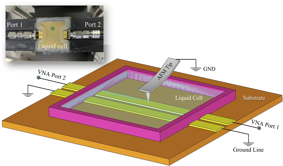
A schematic is reported in Fig. 1 for convenience, along which a picture of the slot-line used in the present paper. The slot-line is printed on a circuit board whose size is 3 cm × 3 cm; it is composed of two gold-coated copper traces 200 μm wide and spaced 100 μm. Electrodes are made of 15 μm of copper, 5 μm of nickel, and 0.03 μm of gold sitting on 512 μm of a low loss material featuring a 2.79 dielectric constant and 0.0019 tan![[thin space (1/6-em)]](https://www.rsc.org/images/entities/char_2009.gif) δ. The device is stacked on a ground plane and some FR4 is added to make the structure more rigid. The liquid container is a small plastic chamber containing liquid 0.3 cm in depth, and a total amount of 1.8 mL. The grounded metal microscope probe then perturbs the waveguide field as it scans the sample. Measurements on the waveguide are performed by a Vector Network Analyzer (VNA), a device able to recover the magnitude and phase of the scattering matrix S, whose elements Sij are the reflected (Sii) and transmitted (Sij) signals between ports i and j. By conducting a scan and recording the plane position of the probe (x,y) along with the corresponding reflected (S11(x,y)) and/or transmitted (S21(x,y)) signals at the waveguide ports, the sample electromagnetic properties can be extracted. In fact, the combined sample and grounded probe act as a shunt admittance function of (x,y) with respect to the transmission line that models the waveguide. iSMM has the advantage of being simple to implement since any existing scanning microscope can be converted into an iSMM by properly designing a sample holder. The method is especially appealing in scenarios where the sample is immersed in a liquid environment, as it does not need any specific probe requirements. It should be stressed that probes for standard SMM are often carefully micromachined microwave devices, incompatible with the in-liquid operation. In this framework, accurate calibration is a fundamental step for the quantitative characterization of both SMM and iSMM. Calibration is necessary to remove unwanted effects such as the probe feedline, the cables, and the connectors. The modeling of undesired phenomena involves the computation of an error matrix containing unknown elements, which necessitates the determination of these elements through a series of raw measurements conducted on known samples, commonly referred to as standards. The most precise approach is to use the capacitance of the probe tip over a ground plane as the known termination impedance of the microscope,3 the ending part of the tip assumed to be a metal sphere. Sometimes a more complex geometry, closer to reality, is assumed for the probe modeling.4 In a lossy liquid, a resistive element in parallel with the capacitor called “spreading resistance”, appears. This paper aims to characterize and illustrate the influence of this specific element on the calibration of microwave microscopy measurements in lossy liquid media. Although the presented results refer to our iSMM, the entire procedure works on standard SMM setups. The proposed expressions can be exploited in other fields than microscopy, such as sensor design.
δ. The device is stacked on a ground plane and some FR4 is added to make the structure more rigid. The liquid container is a small plastic chamber containing liquid 0.3 cm in depth, and a total amount of 1.8 mL. The grounded metal microscope probe then perturbs the waveguide field as it scans the sample. Measurements on the waveguide are performed by a Vector Network Analyzer (VNA), a device able to recover the magnitude and phase of the scattering matrix S, whose elements Sij are the reflected (Sii) and transmitted (Sij) signals between ports i and j. By conducting a scan and recording the plane position of the probe (x,y) along with the corresponding reflected (S11(x,y)) and/or transmitted (S21(x,y)) signals at the waveguide ports, the sample electromagnetic properties can be extracted. In fact, the combined sample and grounded probe act as a shunt admittance function of (x,y) with respect to the transmission line that models the waveguide. iSMM has the advantage of being simple to implement since any existing scanning microscope can be converted into an iSMM by properly designing a sample holder. The method is especially appealing in scenarios where the sample is immersed in a liquid environment, as it does not need any specific probe requirements. It should be stressed that probes for standard SMM are often carefully micromachined microwave devices, incompatible with the in-liquid operation. In this framework, accurate calibration is a fundamental step for the quantitative characterization of both SMM and iSMM. Calibration is necessary to remove unwanted effects such as the probe feedline, the cables, and the connectors. The modeling of undesired phenomena involves the computation of an error matrix containing unknown elements, which necessitates the determination of these elements through a series of raw measurements conducted on known samples, commonly referred to as standards. The most precise approach is to use the capacitance of the probe tip over a ground plane as the known termination impedance of the microscope,3 the ending part of the tip assumed to be a metal sphere. Sometimes a more complex geometry, closer to reality, is assumed for the probe modeling.4 In a lossy liquid, a resistive element in parallel with the capacitor called “spreading resistance”, appears. This paper aims to characterize and illustrate the influence of this specific element on the calibration of microwave microscopy measurements in lossy liquid media. Although the presented results refer to our iSMM, the entire procedure works on standard SMM setups. The proposed expressions can be exploited in other fields than microscopy, such as sensor design.
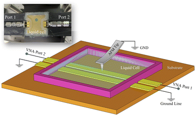 |
| | Fig. 1 Schematic of an AFM-based iSMM: a planar waveguide – either a coplanar waveguide or a slot line – is used as a sample holder. Reflection and transmission coefficients are measured while a conductive grounded tip is scanned across the sample perturbing the field. The whole AFM tip is immersed in liquid (note: several details are not shown to simplify the schematic). (inset) Picture of the slot-line used in the reported experiments, highlighting the plastic container for liquid. | |
Theory
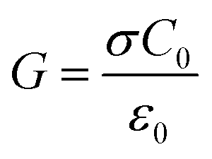
In the calibration procedure described in ref. 3 the known load was constituted by the capacitance of a sphere, modeling the ending part of the probe, over a metal plane evaluated by recursive images5| |
 | (1) |
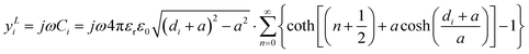
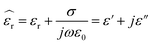
being a the radius of the sphere and di its i-th distance from the ground. Incidentally, the image method was also used by Gao and Xiang6 to relate the shift in the resonant frequency of a kind of SMM to the dielectric constant of the sample. Note, the quasi-static hypothesis holds by virtue of the “near-field” operation of the microscope. Here the dielectric constant εr is the one of the surrounding medium, and more generally, when a homogeneous medium with relative dielectric constant εr fills the space surrounding the probe, we will have simply,where C0 is the corresponding capacitance in vacuum. When the medium has a conductivity σ, the capacitance is no longer solely sufficient to accurately model the system, since a spreading admittance appears in parallel. Calculation of the spreading admittance would require solving a Laplace equation; however, the same equation and the same potential distribution is implied in the calculation of C0 so that C0 already embeds information about the spatial distribution of the electric field. In general, by fundamental electromagnetic theory, the relative dielectric constant can be replaced by the complex dielectric constant,| |
 | (3) |
and the spreading admittance G simply arises from the imaginary part of the complex capacitance (2) when (3) is used, namely,| |
 | (4) |
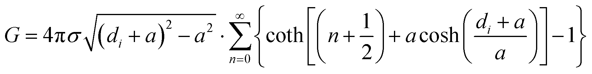
In the case of the sphere, by virtue of (1) we have
| |
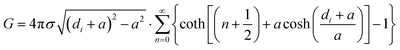 | (5) |
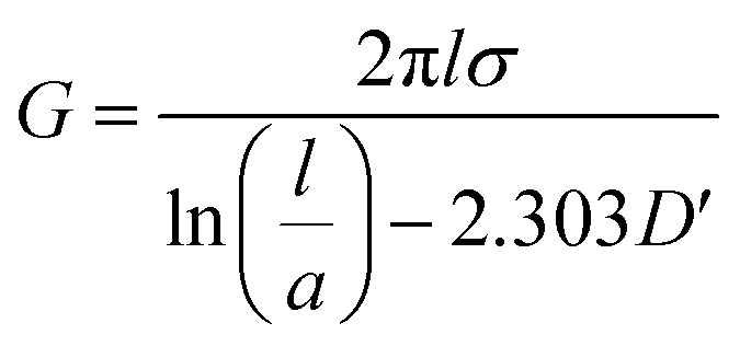
The above approach can be quickly extended to other shapes. For example, a set of approximate expressions is reported for different shapes,7 including a vertical finite wire of radius a and length l at distance d from the ground, so that by our approach we would get,
| |
 | (6) |
where
D′ is a numerical coefficient that can be interpolated from a table as a function of
d/
l. To simplify its use, we have calculated a possible polynomial interpolation, as
| | |
D′ = 0.411 − 0.746x + 1.346x2 − 1.355x3 + 0.731x4 − 0.204x5 + 0.027x6 − (1.228 × 10−3) x7
| (7) |
where
x =
d/
l.
Experimental
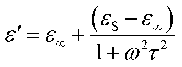
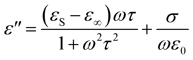
To calibrate SMM measurements in DMEM, we have fitted the measurements reported in ref. 8 in the frequency range of 1–9 GHz to a single-pole Debye model and extracted the conductivity from the imaginary part of the dielectric constant. Single-pole Debye model for salty liquid can be expressed as9| |
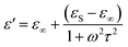 | (8) |
| |
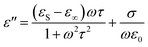 | (9) |
and results of fitting are shown in Fig. 2 with fitting parameters ε∞ = 10.752, εS = 75.142, σ = 1.412 [S m−1] and τ2 = 9.05 pS, valid at 23 °C.
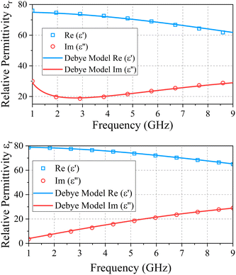 |
| | Fig. 2 Comparison between real and imaginary part of (top) DMEM and (bottom) distilled water permittivity as measured in ref. 7 and as fitted by eqn (8) and (9). Parameters in the text. | |
It appears that DMEM is strongly dispersive, especially in the lower frequency range, where ionic contribution is dominant.
Most importantly, the sensitivity of microwave microscopes appears generally at a much lower frequency in liquid, because of the reduction in wavelength, and consequently, a correct model of the dispersive behavior becomes relevant.
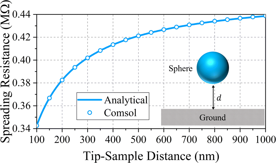
Results predicted by eqn (5) and a Finite Element Methodology (FEM) based 2D axis-symmetric simulation by the commercial software COMSOL are shown in Fig. 3; here the radius of the sphere is assumed to be 100 nm, and simulation is performed at 1.5 GHz where the DMEM medium is particularly highly dispersive and the conductivity is assumed to be σ = 1.732 S m−1; in the simulation, the distance between sphere and ground is varied from 100 nm to 1 μm.
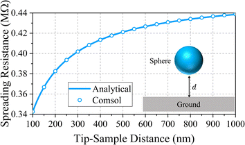 |
| | Fig. 3 Comparison of spreading resistance calculated from eqn (5) and from COMSOL for a sphere in DMEM at 1.5 GHz. | |
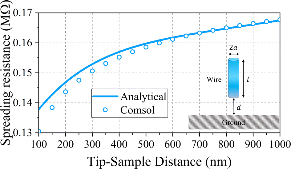
By the same token, Fig. 4 compares the COMSOL results with eqn (6) for a cylindrical wire 1 μm long, with a radius of 100 nm, and conductivity as in the previous example.
 |
| | Fig. 4 Comparison of spreading resistance calculated from eqn (6) and from COMSOL for a cylinder in DMEM at 1.5 GHz. | |
Note, while prediction for the sphere is extremely accurate, since eqn (1) is rigorous, the case for a cylinder was recovered from an approximate expression, and some deviation between COMSOL and the analytical model was expected. In accordance with the methodology described in ref. 3 and, ref. 10 the calibration of S11 measurements is performed on an inverted microscope configuration. The microscope consists of a slot-line structure, described in the introduction, serving as a sample holder for an AFM (NT-MDT SMENA, equipped with a in-liquid head) as shown in Fig. 1. Simultaneous recordings of S11 and S21 are conducted using a VNA (Keysight E8361A) operating at an intermediate frequency (IF) of 100 Hz and a power level of −15 dBm. Throughout the measurements, a platinum-coated cantilever AFM probe (Rocky Mountain Nanotechnology 12Pt400B) with a radius less than 8 nm is systematically displaced at various distances from the metal line. The probe tip is assimilated to a sphere (8 nm radius). Capacitance and conductance are calculated using expressions (1) and (5), considering the presence of DMEM liquid modelled by eqn (8) and (9). They are used as known loads at three distances to calibrate measurements at the remaining distances.
Results and discussion
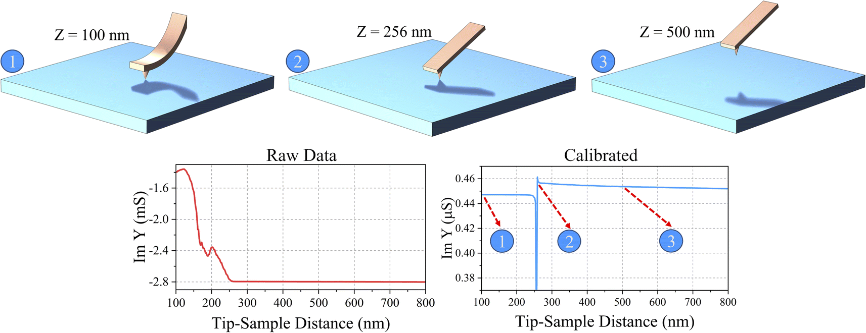
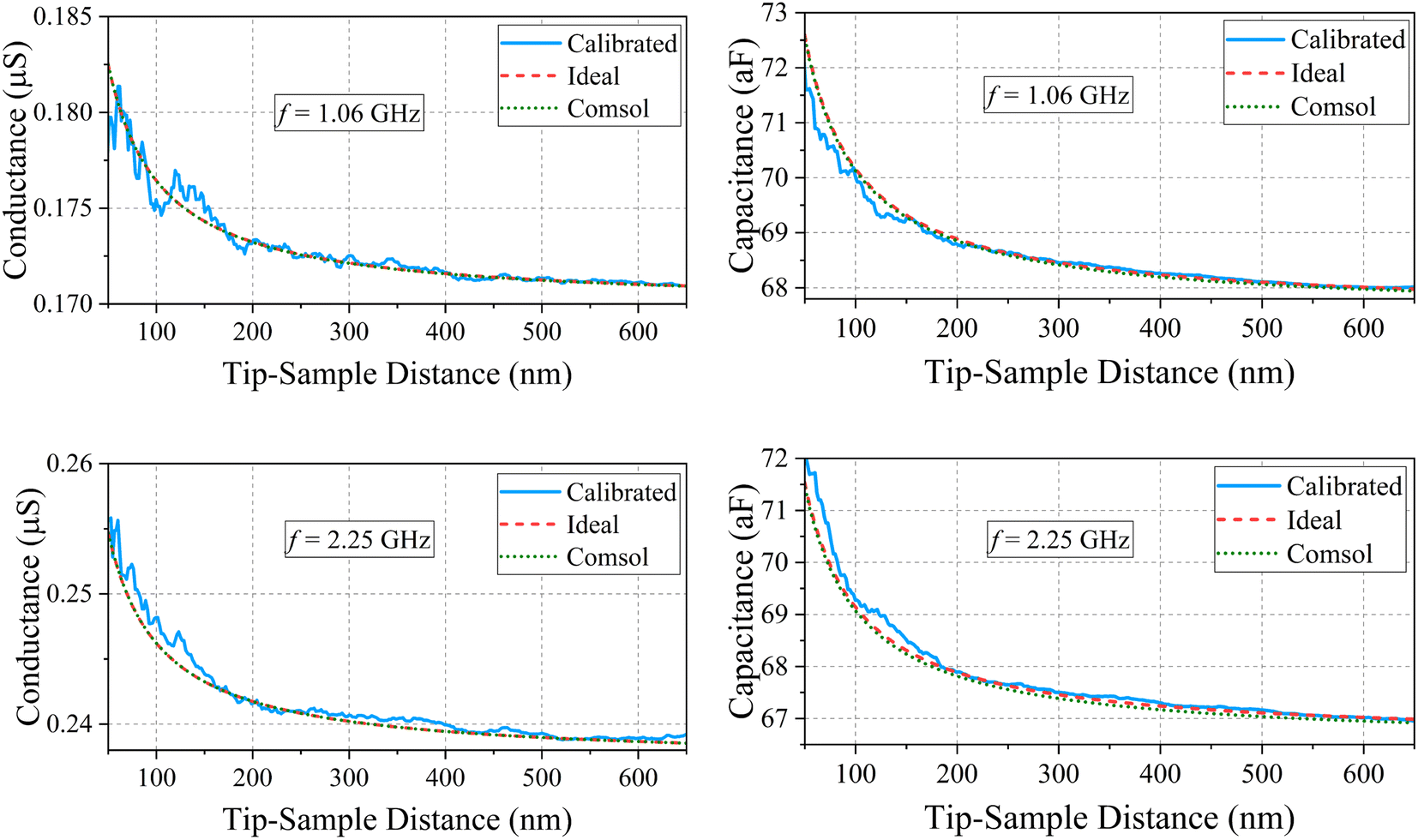
One of the main problems to evaluate the probe-sample admittance correctly and accurately is to understand at which distance the probe touches the sample holder, basically the “zero” of the measurement in terms of distance; in fact, the electrical effect of the contact seen at the input of a complex error network is not easily predictable at high frequencies. To further complicate the measurements, there are additional effects, such as the known hysteresis in tip approaching/retracting after contact, due to sticking effects, and the possible bending of the probe when close to the metal line, due to electric forces. Such effects are not an issue when calibrating STM-based microscopes, owing to the rigid probe, but can make useless the measurements of an AFM-based SMM. To the best of our knowledge, this problem has not been discussed before, and in the following, we introduce a possible solution. To locate the zero, we have made a first rough guess based on the nominal vertical position of the probe z = 0 (available from the AFM microscope and corresponding to the landing quote), and we have calibrated the input admittance using the admittance of a sphere at three probe-sample distances, measured assuming this zero. In this condition, depending on the AFM setting point, at z = 0 the cantilever is significantly deflected, as shown in the top left schematic of Fig. 5, position numbered 1; hence, after opening the feedback loop and retracting the probe, the latter will remain in contact with the sample even when the piezo actuator extends for tens to hundreds of nanometers (top center schematic of Fig. 5, position numbered 2). On the other hand, to correctly evaluate the sphere/metal distance, the zero must be located where the probe switches from a contact to a contactless condition. After this first tentative calibration, a strong discontinuity was clearly visible in the calibrated input admittance at some position z = z0. This is summarized in Fig. 5, where discontinuity is near 256 nm. Next step was assuming z0 as reference point, namely the actual zero, and raw data were calibrated again using the corrected distances. The final results are reported in Fig. 6 for both conductance and capacitance as function of the tip-line distance, at 1.06 GHz and 2.25 GHz. Note, this measurement was simultaneously performed at 100 frequency points between 1 and 3 GHz. If the calibration is correct, the behavior of the curve should perfectly follow the ones predicted by eqn (1) and (5). The obtained results are in excellent agreement, with the capacitance measurement exhibiting higher accuracy. This observation aligns with the fact that while losses are noticeable, they are not excessively high, resulting in slightly reduced accuracy in the measurements of the real part of the input admittance.
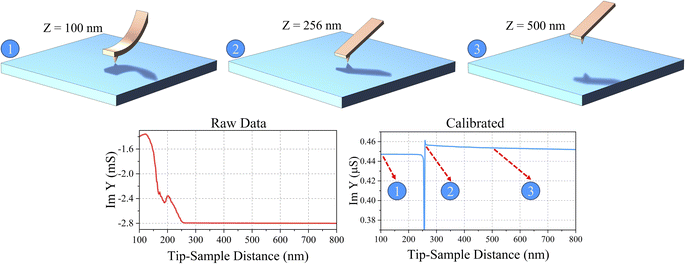 |
| | Fig. 5 Top: illustration of the three scenarios of the probe switching from a contact to a contactless condition; bottom left, raw input admittance; bottom right, (first attempt – see text for more details) calibrated input admittance. | |
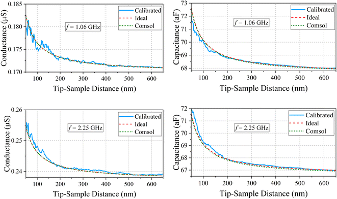 |
| | Fig. 6 Top left: comparison between expected ideal, COMSOL and measured conductance in DMEM with a sphere 8 nm of radius, after calibration at 1.06 GHz as a function of the probe-metal distance; top right, same comparison for the capacitance; bottom left, comparison for the conductance at 2.25 GHz and bottom right comparison for the capacitance. | |
Same measurements were performed for the distilled water, where Debye fitting parameters to ref. 8, that coincide remarkably with what reported in ref. 9 at 23 °C, are ε∞ = 5.14, εS = 79.11, σ = 0 and τ = 8.50 pS. Fitting parameters for both DMEM and distilled water are summarized in Table 1.
Table 1 Debye fitting parameters for DMEM and distilled water
| Material |
εs |
ε∞ |
σ [S m−1] |
τ [pS] |
| DMEM |
75.412 |
10.752 |
1.412 |
9.05 |
| Distilled water |
79.11 |
5.14 |
0 |
8.5 |
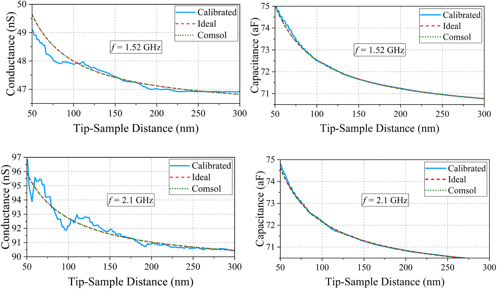
The final results are reported in Fig. 7 at 1.52 and 2.1 GHz. In this case, the conductance measurement is inherently noisier due to its lower value. Nonetheless, the reduced losses enabled a more precise measurement of the capacitance.
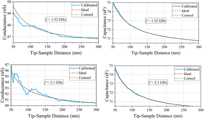 |
| | Fig. 7 Top left: comparison between expected ideal, Comsol and measured conductance in distilled water with a sphere 8 nm of radius, after calibration at 1.52 GHz as a function of the probe-metal distance; top right, same comparison for the capacitance; bottom left, comparison for the conductance at 2.1 GHz and bottom right comparison for the capacitance. | |
Conclusions
In conclusion, this study presents a straightforward yet effective approach for assessing the spreading resistance of electrodes with diverse shapes immersed in a lossy medium, specifically in saline liquids. In this framework, a Debye model for DMEM, a widely used medium for biological applications, is developed. The derived expressions for spreading admittances are rigorously validated against finite element simulations and subsequently employed in the calibration of probe measurements conducted within a lossy biological buffer, such as DMEM, using an inverted scanning microwave microscope. Results are useful for calibration of any kind of scanning impedance microscope and could be also used in domains different than microscopy, such as fluidic sensors.
Author contributions
Marco Farina conceptualization, investigation, methodology, software, supervision, validation, writing – original draft; C. H. Joseph formal analysis, visualization, investigation, writing – original draft; S. N. Afifa Azman data curation, investigation; Antonio Morini conceptualization, writing – review & editing; Luca Pierantoni funding acquisition, project administration; Davide Mencarelli supervision, investigation, writing – review & editing, Andrea di Donato writing – review & editing, Tiziana Pietrangelo resources, writing – review & editing; Richard Al Hadi investigation, writing – review & editing.
Conflicts of interest
There are no conflicts to declare.
Acknowledgements
This research was supported by the European Project H2020 FETPROACT- EIC-05-2019 “NANO-EH” under GA No. 951761.
References
- S. M. Anlage, V. V. Talanov and A. R. Schwartz, Principles of Near-Field Microwave Microscopy, Springer, New York, NY, 2007, pp. 215–253 Search PubMed.
- M. Farina, X. Jin, G. Fabi, E. Pavoni, A. di Donato, D. Mencarelli, A. Morini, F. Piacenza, R. Al Hadi, Y. Zhao, Y. Ning, T. Pietrangelo, X. Cheng and J. C. M. Hwang, Appl. Phys. Lett., 2019, 114(9), 093703 CrossRef.
- M. Farina, D. Mencarelli, A. Di Donato, G. Venanzoni and A. Morini, IEEE Trans. Microwave Theory Tech., 2011, 59(10), 2769–2776 CAS.
- G. Gramse, M. Kasper, L. Fumagalli, G. Gomila, P. Hinterdorfer and F. Kienberger, Nanotechnology, 2014, 25(14), 145703 CrossRef CAS PubMed.
- W. R. Smythe, Static and Dynamic Electricity, McGraw-Hill, New York, 2nd edn, 1950 Search PubMed.
- C. Gao and X.-D. Xiang, Rev. Sci. Instrum., 1998, 69, 1998 Search PubMed.
- J.-R. Riba and F. Capelli, Energies, 2018, 11(5), 1090 CrossRef.
- X. Jin, M. Farina, X. Wang, G. Fabi, X. Cheng and J. C. M. Hwang, IEEE Trans. Microwave Theory Tech., 2019, 67(12), 5438–5445 Search PubMed.
- Y. A. Gezahegn, J. Tang, S. S. Sablani, P. D. Pedrow, Y. K. Hong and H. Lin, et al., Innovative Food Sci. Emerging Technol., 2021, 74, 102837 CrossRef CAS.
- G. Fabi, X. Jin, E. Pavoni, C. H. Joseph, A. Di Donato, D. Mencarelli, X. Wang, R. Al Hadi, A. Morini, J. C. M. Hwang and M. Farina, IEEE Trans. Microwave Theory Tech., 2021, 69(7), 3348–3359 Search PubMed.
|
| This journal is © The Royal Society of Chemistry 2023 |
Click here to see how this site uses Cookies. View our privacy policy here. 
 Open Access Article
 This Open Access Article is licensed under a Creative Commons Attribution-Non Commercial 3.0 Unported Licence
 *a,
C. H. Joseph
*a,
C. H. Joseph