
 Open Access Article
 This Open Access Article is licensed under a Creative Commons Attribution-Non Commercial 3.0 Unported Licence
The role of lanthanide luminescence in advancing technology
Gabriella Tessitore†
 *ab,
Gabrielle A. Mandl†a,
Steven L. Maurizioa,
Mannu Kaura and
John A. Capobianco*a
*ab,
Gabrielle A. Mandl†a,
Steven L. Maurizioa,
Mannu Kaura and
John A. Capobianco*a
aConcordia University, Department of Chemistry and Biochemistry & Center for NanoScience Research, 7141 Rue Sherbrooke Ouest, Montreal, QC, Canada. E-mail: john.capobianco@concordia.ca
bDepartment of Chemistry, Université Laval, 1045 Av. de la Médecine, Québec, QC, G1V 0A6 Canada. E-mail: gabriella.tessitore@chm.ulaval.ca
First published on 13th June 2023
Abstract
Our society is indebted to the numerous inventors and scientists who helped bring about the incredible technological advances in modern society that we all take for granted. The importance of knowing the history of these inventions is often underestimated, although our reliance on technology is escalating. Lanthanide luminescence has paved the way for many of these inventions, from lighting and displays to medical advancements and telecommunications. Given the significant role of these materials in our daily lives, knowingly or not, their past and present applications are reviewed. A majority of the discussion is devoted to pointing out the benefits of using lanthanides over other luminescent species. We aimed to give a short outlook outlines promising directions for the development of the considered field. This review aims to provide the reader enough content to further appreciate the benefits that these technologies have brought into our lives, with the perspective of travelling among the past and latest advances in lanthanide research, aiming for an even brighter future.
1 Introduction
For a long time after their discovery, lanthanides did not initially find a suitable application, despite their far-reaching technological use in our quotidian.1–4 The first real barrier to any practical use of such elements was their similar ionic radii in their most common trivalent form. Their similar sizes impacted each step of their discovery process, even during the initial attempts to simply identify the whole lanthanide series upon their extraction from minerals like gadolinite, first discovered in the 1790s. Due to the similarities between these elements, some of their mixtures were initially confused for a single new element. It took almost two centuries of research to finally confer these elements their rightful place on the periodic table.Their reputation as rare earths is also somewhat misleading. Most of the lanthanides are indeed among the least abundant metals on Earth, but they are all more abundant than gold.5 Moreover, the presence of some of the lanthanides in minerals is far from scarce, such as cerium, neodymium and lanthanum. Cerium is almost as abundant as zinc, which is considered a relatively abundant element. The label “rare” confers a sense of preciousness to the lanthanides, which is well represented by their relatively high cost compared to other elements of similar abundance. Because lanthanides are not concentrated in a single ore, their extraction is difficult, resulting in supply chain disruptions in past decades.6 These factors, more than their relative abundance, brought about a sense of uncertainty in the industries relying on them. This uncertainty, in combination with their relatively high cost, resulted in industries seeking out alternative elements.
Financial factors have a significant impact on the commercialization of a novel technology. From a cost-benefit aspect, the inclusion of lanthanides into otherwise affordable and functioning technologies might not represent an advisable route to improving them. For example, cost-benefit concerns for using lanthanides are probably not a significant issue for a billion-dollar aerospace mission, while the benefits achieved by a lanthanide-based photocatalyst in wastewater treatments may not be enough to counterbalance the cost of the proposed purification system. This review focuses on applications in which the technologies benefitting from lanthanide luminescence reached widespread commercial use.
Despite their drawbacks, lanthanides are part of multiple inventions which have become essential in modern society.7–11 More common applications of the pure lanthanide metals are in metallurgy, ceramics, and catalysis, while the magnetic and optical properties of the di-, tri- and tetravalent ions are exploited in various industries. The versatility of lanthanide-based luminescent materials in terms of the possible excitation sources and luminescence wavelengths, lifetimes and band characteristics explains the reasons behind their broad use in many fields that rely on light.12–15 Extensive reviews about the luminescence mechanisms of lanthanide ions in different oxidation states can be found elsewhere.7,10
Importantly, the reported technologies are in actual use or, at minimum, their use in patented prototypes has already been demonstrated. Although there are many prospective new technologies reported in the academic literature that may one day become staples in future society, the aim of this review is to outline the advancements that have made our current lanthanide-based technologies possible. Nevertheless, prospective promising applications are provided for each section. Finally, we provide in-depth descriptions only of technologies relevant to modern times, with the ambition to inspire the future of the field by providing the most successful examples of our era.
2 Lanthanides in lighting and displays
2.1 Early uses of phosphors: incandescence, fluorescence and cathodoluminescence
The beginning of the modern era is often thought to coincide with the advent of artificial, or electric, illumination in the 19th century. The creation of the first light bulb was developed by Joseph Wilson Swan, and improved upon by the likes of Edison, Thompson, and Tesla among others.16 The electric arc light was also introduced around this time.17Simultaneously, there were other types of electrical lighting being explored, as the efficiency of the incandescent lamp is limited by its own resistive nature: incandescence occurs by thermal conversion of electricity caused by the resistance of the material. Thus, much of the energy is dissipated as heat rather than light. Electrical lighting based on gas-discharge was first observed during the 17th century and was continually studied and improved upon because of its higher efficiency than incandescence.18 Moreover, the invention of the discharge lamp resulted in less dissipative and more efficient light conversion, at the initial disadvantage of producing light at hues not suitable for indoor illumination.19 For example, mercury lamps give off a strong blue-green light, along with UV light. In order to further their commercialization, it was necessary to first correct the emission chromaticity by the use of luminescent materials, known as phosphors (Fig. 1). To achieve this, the blue-green emissions of mercury lamps were combined with red phosphors to achieve white light by means of exciting the red phosphors with the residual UV emissions from mercury.19 Thus, the fluorescent lamp was born, consisting of a lamp made by combining a UV-emissive metal (typically mercury vapor), a noble gas (argon at first) to generate current through, and a visible-luminescent phosphor. The first versions were patented by Edmund Germer in 1927, who later licensed his invention to the General Electric Company.20 The possibility to harness the UV emissions from gas discharge lamps and further convert them to visible emissions has kept these types of lamps in widespread use, even after the commercialization of more efficient technologies, like light-emitting diodes (LEDs). It is in the search for efficient and appropriate lighting that lanthanide-based phosphors became an important part of fluorescent lighting technologies.
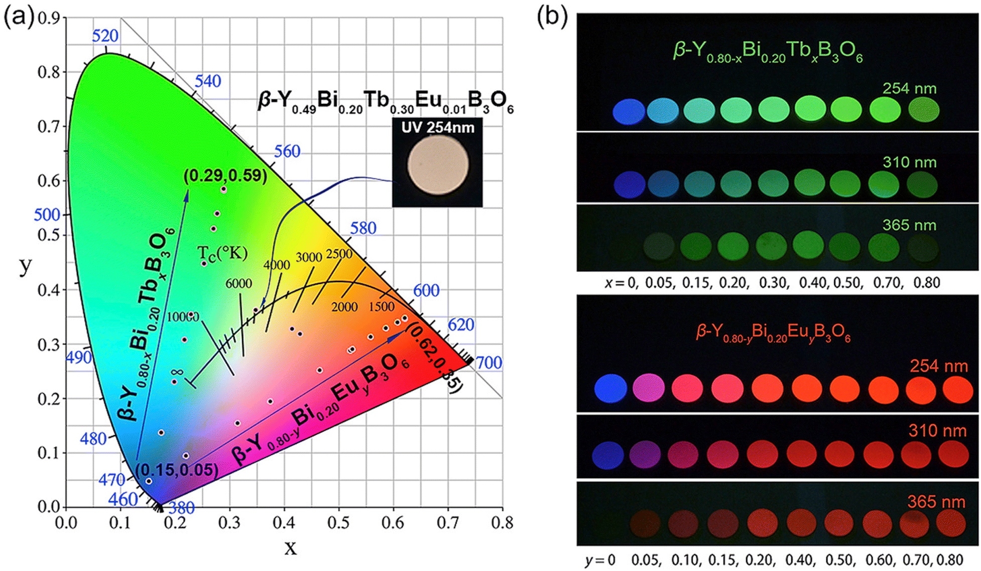 | ||
| Fig. 1 (a) 1931 Commission Internationale de l'éclairage (CIE) diagram and corresponding positions of Eu3+ and Tb3+-doped phosphors as a function of colour temperature and purity. The inset shows a white light phosphor under UV excitation at 254 nm. (b) The range of emission colours achieved by doping β-YBiB3O6 with different amounts of Tb3+ (top) and Eu3+ (bottom) under 254, 310 and 365 nm UV wavelengths. Reproduced with permission from ref. 29. | ||
Similarly, conversion to visible light is required when using a cathode-ray tube (CRT).21 In a CRT, an electron gun generates a flow of charges, which can be deviated by the use of magnetic fields to hit a specific target on a screen. Such technology was mainly exploited in the production of televisions and instruments for the determination of wave behaviour, e.g. the oscilloscope. The conversion of the electron beam into luminescent signal on the screen must be achieved by the use of materials capable of generating charge carriers whose recombination provides luminescence, like in the LEDs described in Section 2.3. Lanthanide-based phosphors were particularly instrumental in bringing about CRT display technologies, especially in colour. Cathodoluminescence involves the transformation of electrons with high energy to light.19
Although the application of the phosphors in fluorescent lamps and CRT take advantage of different luminescence phenomena, the choice of the lanthanide phosphors is similar among all the different applications. The first commercial lanthanide-based phosphor was YVO4:Eu3+, introduced in 1965 by General Telephone & Electronics laboratories, for the purpose of using it in CRT-based colour television.22 The 1960s have been referred to as the “golden age” of lanthanide phosphors, as most of the commercial ones were discovered during that time.23 The production of lanthanide-based phosphors has not changed significantly over time, both because of the relative recency of their commercialization, and also because of the recent efforts to replace such phosphors with ones that are less affected by supply chain issues. When these technologies were proposed, lanthanides were still easily and reliably obtained.
The lanthanides played an undeniable role in producing CRT colour displays using a triphopshor system.24 In this technology, the lanthanides brought about a high degree of colour purity, essential for producing realistic images. Briefly, in such an invention, a combination of three separate blue, green, and red phosphors are used in tandem to allow for a better colour rendering by taking into account the trichromatic perception of the human eye. The red-green-blue principle is still applied in the most recent display technologies.
Lanthanide phosphors can be made from a variety of different host materials.21,25–29 The majority of blue light phosphors are based on the emissions from Eu2+ in several host materials, such as aluminates and chloroapatites. Green phosphors rely on the emissions from Tb3+ in oxysulfides and garnets, while red phosphors are commonly Eu3+-doped oxides, phosphates, aluminates, oxi-chalcogenides, borates and sulfates. The phosphor set known as P22 was perhaps the most widely used tricolour set in commercial CRT monitors, where Y2O2S:Eu3+ represented the red component of the set.30,31 In the decades since their introduction, CRT displays currently occupy a niche market, owing to the relative bulkiness of such devices. Notably, Thomas Electronics currently produces CRT displays and specify YAG:Tb3+, better known as P53, as their default phosphor.32 Since the eyes are well-adapted to detecting green light, monochromatic displays often use simple green phosphors for such a purpose. Most of their CRTs are developed for avionics and marine radar use.
2.2 Lanthanides in light-emitting diodes (LEDs)
Light-emitting devices are all based on the principle of electrical pumping into semiconductor materials, with conversion of electric energy into luminescence.33–35 Charge carriers can recombine as an excitonic emission, or via luminescent centers, which can be intrinsic to the semiconductor material or added as a dopant in the emissive layer; lanthanides have been used as dopants for this purpose.34–36 The first blue LED was patented in 1973, based on GaN.37 Today, the blue light from LEDs is mostly based on InGaN, which is in widespread use. This is what gives rise to the predominant blue emissions in modern colour displays. Rather than developing LEDs with intrinsic emissions of different colours, research has been devoted to finding ways to alter blue LEDs to emit other colours simultaneously, generating white light. The use of luminescent centers capable of such a conversion is the reason for the massive use of lanthanides in modern displays and LED lighting.Lanthanides are used in LEDs either by doping the semiconductor active layer to transform its emission wavelength, or by coating the layers with lanthanide-based phosphors that are capable of absorbing the light emitted by the chosen LED and emitting a desirable visible wavelength.34–36 The latter strategy was predominately used for the development of white light LEDs, which currently relies on lanthanide phosphors to achieve a range of white light colour temperatures.38
LEDs produced by direct doping of the semiconductors take advantage of the sharp emission lines of Eu3+ and Tb3+ to achieve colour purity, or the broadband emissions from Eu2+ and Ce3+ to obtain white emissions.34–36 More commonly, phosphors are coated on top of the LEDs, avoiding direct contact with the active layer. In such a system, the phosphor simply re-absorbs the emitted light, which reduces the loss of the intrinsic emission from the semiconductor material. However, the spatial separation between the emitting semiconductor material and the lanthanide phosphor results in a lower absorption efficiency, dictated by the limited extinction coefficients of the lanthanide ions. If the two were in closer proximity, such limitations could be overcome by non-radiative energy transfer among the semiconductor and lanthanide ions, but it would change the semiconductor bandgap, leading to a less efficient intrinsic emission from the LED. Coating is consequently favored over co-doping.
Ce3+-based phosphors present mainly green-yellow emissions, when singly-doped in aluminium garnets, aluminates, silicates and silico-nitrides.39–41 Nitrides,42 sulfides,43 oxynitrides44 singly doped with Eu2+ exhibit blue-green emissions depending on the chosen host. Ce3+ and Eu2+ co-doped silico-nitrides directly allow for the achievement of white light by combining blue light and these broadband emitters in multiple lumiphore layers.64 The proposed structure allows for the interactions between successive layers, with the possibility to change the obtained colour chromaticity by varying the layer thicknesses.
The most efficient LEDs on the market are all based on lanthanide luminophores. Both Creed Inc and Philips reported LED efficiencies higher than 200 lm W−1 by the use of the very same technology described herein.38 With respect to the common layering approach of different phosphors, Philips took a different approach to obtain its most efficient LED.45 Using the light from InGaN, the blue emission is converted to green light by a luminophore containing Eu2+ and Ce3+. Separately, a red LED is stacked, to achieve the final white emission with ultra-high intensity. The proposed architecture differs significantly from the others, which reported layering luminophores rather than alternating LED and luminophore layers. Such a successful case might move the industry in combining multiple point sources rather than using individual luminophores, which are still crucial for the LED industry.
With regard to displays, the Eu3+-based red LEDs have become prominent. Even with the advent of liquid crystal displays (LCDs), incorporated lanthanide phosphors were still based on the same materials previously in development, with particular interest in vanadates and oxysulfides.46 The further development of display technology is currently pointing towards organic materials, which results in the tendency to dismiss inorganic-based lumiphores for LED displays.
Despite these advancements, lanthanide luminescence is hindered by their intrinsic low absorption cross-sections. Current research is being carried out towards improving this by taking advantage of the antenna effect, through the use of ligands capable of absorbing the LED light and transferring it to the lanthanide luminescent center.47,48
2.3 Future perspectives on lighting and phosphors
Hybrid organic-LEDs (OLEDs) based on lanthanides are surely interesting materials for applications in lighting and displays.49–51 The OLEDs have almost completely replaced LEDs, due to their higher performance in terms of resolution and colour rendering. Considering the strong electroluminescence efficiency of many lanthanide complexes, it seems counterintuitive that the OLED industries do not yet employ lanthanide-OLEDs in their current products on the market.52–54 Likely, this is due to supply chain insecurities, though this may be remedied in the future as more lanthanide mining operations become active worldwide.9 Regardless, lanthanides are uniquely able to achieve high colour purities due to their energy level structure, while obtaining high quantum efficiencies of the photon conversion process. These particularities are unique to the lanthanide series, which renders an auspicious future for the development of this sector.3 Light amplification by the stimulated emission of radiation (LASER)
Trivalent lanthanides have constituted the luminescent center in the gain medium of many solid-state lasers. Introduced in 1962, the third laser produced was based on Nd3+ ions.55 The development and applications of lasers, both on Earth and in space, are continuously booming, with a widespread involvement of the lanthanide ions in these technologies. The use of non-linear optics, different hosts, and activators produced a plethora of available laser technologies, with emissions ranging from the VUV to the NIR.56,57Independently of the pumping source, whether electrical or photonic in nature, the functioning of a laser requires the excitation of the activator in the gain medium, which can either relax radiatively via spontaneous or stimulated emission.57,58 Stimulated emissions require a photon of the pumping source to interact with photons in an excited state to obtain an emission, coherent with the pumping source. Both spontaneous and stimulated emissions can occur in an activator, and the probability of obtaining the required stimulated emission increases with the lasing wavelength.59 Thus, lanthanides with emissions in the NIR represent the most efficient activators for lasers, with Nd3+-doped yttrium aluminum garnet (Nd:YAG) being one of the most commonly used lasers since its invention in 1964 by Joseph Geusic and LeGrand Van Uitert at Bell Telephone Laboratories.60 As shown in Fig. 2, the Nd:YAG laser has a main emission at 1064 nm, but is also used in its frequency doubled, tripled and quadrupled forms at 532, 355 and 266 nm, respectively.
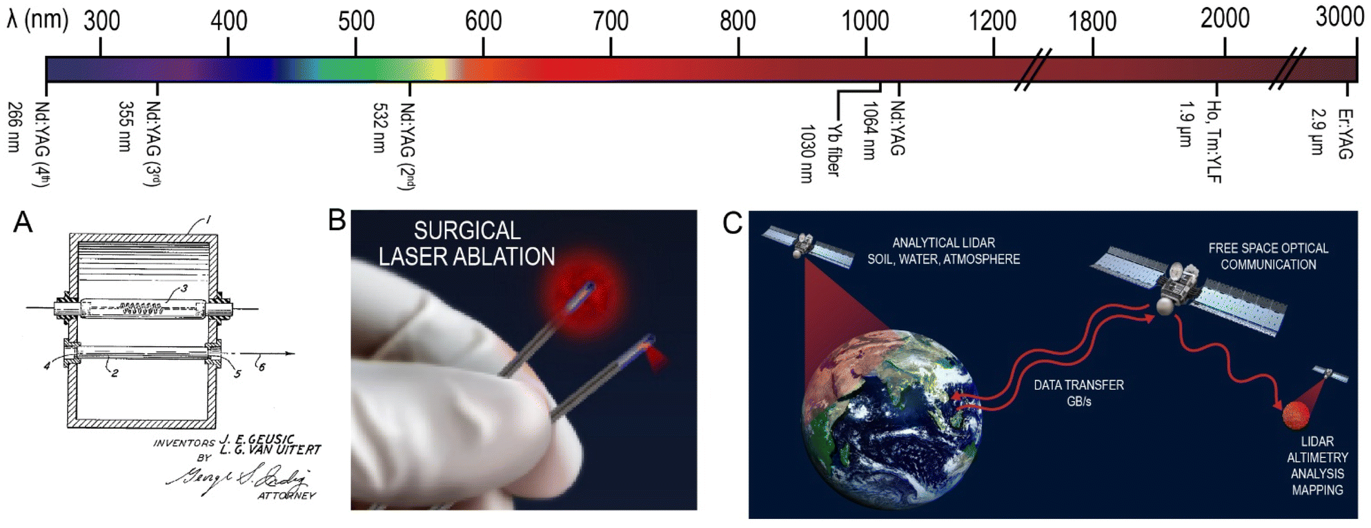 | ||
| Fig. 2 (A) Original schematic of the Nd:YAG laser in the 1964 patent filed by Geusic and Van Uitert. (B) Photograph of the NeuroBlate® system by Monteris, which uses a Nd:YAG laser at 1064 nm for stereotactic laser ablation in neurosurgery. (C) Graphical depiction of the various ways infrared lasers are used in LIDAR and free space optical communication. Figures reprinted from ref. 55 and 82 with appropriate permissions. | ||
The advancements of laser technologies resulted in shortening of the pulse times to the femtosecond range. The superposition of the waves from the pumping laser and the activator emission during lasing determines the laser pulse width. A perfect superposition of the two waves corresponds to continuous conditions, while inversion of the population in a single shorter pulse can be obtained by allowing the build-up of the energy (Q-switching), by the interferences of multiple laser modes (mode locking), by external pumping with a shorter pulse width or by miniaturization of the laser cavity through the use of diodes or optical fibers.61–63 These last two approaches are particularly interesting in view of the opportunity to release high power densities in an ultrafast time span. Nd:YAG lasers are still the most commonly encountered lasers in laboratories worldwide, particularly for their use in spectroscopy. Despite being one of the earliest lasers ever produced, the innovations discussed below promoted further applications than the simple spectroscopic analyses of luminescent materials. Shorter pulses can be achieved in Q-switching mode with the confinement of the cavity offered by the use of fibers or a pumping diode.
The obtained enhanced power and smaller size of the devices are particularly interesting with respect to one of the most common uses for lasers in industry: material ablation. With respect to large-scale ablation, the CO2 lasers are most appropriate. However, the Nd3+ and Yb3+-based lasers have recently received attentions in view of the possibility of using ultrafast lasers, which have been successfully applied to ablation in the micron and nano scale, applied in several industrial production sectors.64–70
3.1 Lasers in surgical procedures
Further opportunities in the medical surgical sector exploit the short pulses as a means of avoiding prolonged invasive treatments by the administration of high-power densities in short, single pulses. Laser ablation is one of the most important surgical advances, taking advantage of a variety of lasers ranging from the UV to NIR. Lasers for ophthalmic surgeries for cataracts were first patented in 1984, and relied on the emissions from nanosecond pulsed Nd:YAG lasers at 1064 nm.71 Since then, femtosecond lasers based on Yb3+ have dominated the market for ophthalmic surgeries, as the faster pulses further minimize tissue damage, at a similar wavelength of 1030 nm.72–75 Skin ablation for possible treatment of epithelial anomalies can also take advantage of Nd3+ and Er3+ NIR lasers at 1064 nm and 2.94 μm, respectively.76–81 The laser irradiation can treat relatively deep tissues, by eliminating the problematic cells, such as in tumor removal (Fig. 2B).82 The same medical approach can be applied to different body areas, as long as the penetration depth of the intervention allows the laser to reach it. Additionally, cosmetic surgeries also exploit laser treatments for ameliorating the appearance of bodily imperfections. Tattoo removal can be achieved through pulsed laser irradiating the area, showing particularly better results when the area is treated with shorter pulses. Notably, the different tattoo pigments are cleared by different laser wavelengths. In this respect, the frequency-doubled 532 nm emission from the Nd:YAG laser has been essential for removing red pigments, while the 1064 nm emission is used for blue and black pigment removal.83,84 Cellulite, aging and scarring are other problems that these approaches are trying to improve, mostly by inducing minor damage to the skin to obtain a boosted production of collagen, which can help with each of these problems; Nd and Er:YAG lasers are primarily used for this purpose in a similar fashion to skin ablation discussed above.85,86 Other aesthetic laser procedures are also available, such as aesthetic dentistry, ablation or hair laser removal.87,883.2 Free space optical communication
Free space optical (FSO) communication also exploits lanthanides for signaling within servers on Earth, or single and bi-directional communication from space. Wireless communications have enabled a global societal connection and facilitated space exploration. To achieve communication of information in free space, NIR laser diodes have been employed in the past, with the aim to transmit an optical signal among relatively close servers.89 Although this technology has been replaced by fiber-coupled systems which guarantee a lower dissipation of the emitted light by amplification of the signal, as presented in Section 6, the reported example resulted in significant implications for achieving communication in space.The advent of laser communication from space began from a simple experiment: the light from an argon laser sent from Earth was detected on the Moon.90 Following this achievement, satellites and Earth bases were equipped with communication systems including lasers, which were devoted to wireless, free-space data transmission. Notably, the 1550 nm emission band from Er3+ is useful for optical communication between bases on earth, but is not ideal for communication to space due to meteorological intereferences.91 With respect to deep space communication, however, the 1064 nm emission from Nd:YAG lasers have been used for communication between NASA terrestrial bases and spacecrafts orbiting Mercury and Mars.92,93 Surprisingly for the time, the emission from the laser was detected at 24![[thin space (1/6-em)]](https://www.rsc.org/images/entities/char_2009.gif) 000000 km from the source, proving that lanthanide NIR lasers could be used for communication in deep space.94 Bidirectional communication was first established using Nd3+-doped lasers for communication, and signals were amplified using Er3+-doped fibers at 1550 nm (see Section 6).95,96
000000 km from the source, proving that lanthanide NIR lasers could be used for communication in deep space.94 Bidirectional communication was first established using Nd3+-doped lasers for communication, and signals were amplified using Er3+-doped fibers at 1550 nm (see Section 6).95,96
Since these first missions, a plethora of satellites equipped with lasers have been sent to space. New challenges arose due to the need to move from near-Earth systems to technologies allowing deep-space communication, which requires high-power lasers designed to achieve long-distance transmissions.97–103 Moreover, the need for the transmission of large amounts of data resulted in the requirement for the lasing transmitting system to achieve a high signal rate. This requirement in part facilitated the creation of high-power and ultrafast laser facilities, like the Shanghai Superintense Ultrafast Laser Facility (SULF).101,102 Similarly, scientists tried to enhance the data transmission rate, which achieved 319 TB s−1 as of 2021 between earth transmission bases.104 Currently, the fastest commercial laser data transmission rates from space are in the GB s−1 range, still employing Nd:YAG lasers.105,106 Only a few of the existing lanthanide-based lasers can fulfil the requirements in terms of power and rate of the signal for space communication, mostly based on previously proven technologies using the NIR emissions of Nd3+ and Yb3+ in diode and fiber lasers.
3.3 Light detection and ranging (LIDAR)
LIDAR takes advantage of laser coherence to determine the topology and/or composition of an environment by measuring the time-of-flight of the reflected signal.89 Although the first laser to show promise for space communication was an argon laser, successive missions to determine the topology of planets like Mercury94 and Mars93 used lanthanide-based laser altimeters based on LIDAR. The possibility to miniaturize lasers and incorporate them into satellites permitted the opportunity to bring analytical spectroscopic equipment to space. It became possible to characterize the soil, water and atmospheric compositions of Earth and other celestial objects via interactions of the incident laser with matter through space LIDAR.107–109 Most of the latest NASA missions using LIDAR employ lanthanide based-lasers, namely Ho3+ and Tm3+ co-doped YLiF4 (Ho,Tm:YLF) or Nd:YAG.109–114 This powerful tool became widely exploited in view of the possibility to monitor atmospheric parameters of the Earth such as pollutant concentrations, aerosol characteristics, wind analysis, and many others, all from space. This achievement provides a unique window for scientists to view the global situation in terms of greenhouse gas emissions and climate change. The pressing need to monitor the concentration of pollutants involved in the perturbation of the photochemistry of the atmosphere justified the necessity for space missions like the recent MERLIN (Methane Remote Sensing LIDAR Mission), which involved lanthanide lasers for methane detection.114In summary, lanthanide-based lasers are ubiquitous, finding uses in a wide variety of industries. As technological advancements continue to be made, it is likely that they will continue to be produced and developed, finding new and potentially unexplored avenues for application.
4 Lanthanides in applications involving ionizing radiation
Radioluminescent materials emit light upon excitation with ionizing radiation. Scintillation is a type of radioluminescence characterized by fast luminescence decay times, on the order of hundreds of ns or shorter.115 Scintillators have found widespread commercial use in detectors for medical imaging, homeland security, radiation safety and high energy physics experiments, among others. The desired properties of a scintillator are largely dependent on the intended application, as such it is well known that there is no single scintillating material that is universally optimal. The main luminescence properties that govern the choice of a scintillator are the emission wavelength, light output (photons emitted per MeV of energy absorbed), energy resolution, proportionality (linearity of emission with absorbed energy), and decay time.116,117Lanthanide-based scintillator materials are among the highest-performing materials, with Ce3+, Tb3+, Pr3+ and Eu2+/3+ in commercial use today (Fig. 3). The commercial success of these lanthanides is attributed to four main properties: their light yields, emission wavelengths, energy resolution, and decay times. Ce3+-doped materials are used for their fast decay times, due to the allowed nature of the 5d → 4f transition of Ce3+, which produces UV or visible light depending on the host material. Unlike the 4f → 4f transitions widely used for lanthanide luminescence, as described in the other sections of this review, the nature of the 5d → 4f transitions of the lanthanides is highly host dependent. For example, YAG:Ce3+ produces emissions at 532 nm, while LaBr3:Ce3+ emits at 360 nm.118,119 The position of the lowest 5d state relative to the conduction band shifts depending on the nature of the host, as described by the centroid shift and red shift models.120 The position of the 5d state of Ce3+, in turn, governs the emission wavelength of the 5d → 4f transition, and consequently the decay time, as the decay time is dependent on the third power of the emission wavelength of this transition.121,122 The lifetimes of Ce3+ materials are among the fastest of the lanthanides, typically 100 ns or less, and can be as fast as 15 ns in the case of LaBr3:Ce3+, or as slow as 150 ns as in Cs2LiLaBr6:Ce3+ (CLLBC), which emits at 420 nm.123,124 The 5d → 4f transitions of Pr3+ are actually faster (<20 ns) than Ce3+ in the same host due to the shift of the 5d levels relative to the conduction band previously discussed.117,122,125 The lowest 5d state of Pr3+ is 1.5 eV lower relative to the lowest 5d level of Ce3+ in the same host, explaining the faster lifetime.120,125 Unfortunately, there are two main disadvantages of the d → f emissions from Pr3+ that have precluded their widespread commercial use. First, a lower light yield is typically obtained (two to three times lower than Ce3+ in the same host) due to de-excitation via a two-step process involving excitation of the 3P0 state, which can also radiatively decay (these emissions are used in radiography, as discussed below).117,126,127 Second, the interconfigurational emissions occur in the deep UV, which are not suitable for use with bialkali photomultiplier tubes (PMTs) and silicon detectors.122,128,129 The 4f65d → 4f7 transition of Eu2+ is also an allowed transition, resulting in some of the highest light yields ever reported (120000 photons per MeV for SrI2:Eu2+) and an emission wavelength of 435 nm. Despite the allowed nature of the 5d → 4f transition, Eu2+ compounds have relatively slow decay kinetics, around 1 μs, due to self-reabsorption.117
 | ||
| Fig. 3 Scintillators are commercially utilized in the form of crystalline arrays, single crystals, and polycrystalline screens. The most prominent lanthanide activators for such materials are Ce3+, Eu2+/3+, Pr3+, Tb3+ and Tm3+. The emissions from these activator ions can be classified by fast decay times (in the ns to ps range) for the allowed 5d → 4f transitions, or by slower decay times in the μs to ms range from the forbidden 4f → 4f transitions. | ||
Afterglow, which is most generally defined as an additional, unwanted slow component to a decay time, is a major drawback to many materials and can severely limit their application.130 While the primary decay time may be very fast, a secondary afterglow decay can cause imaging artifacts and limit detection speeds.117,130,131 Afterglow is generally caused by the presence of trapping states that are introduced alongside defects in the crystalline material. In the case of materials that are intentionally doped with an activator ion (as is the case in most lanthanide-based scintillators), the introduction of these defects is unavoidable. In some cases, however, one can take advantage of the presence of trapping states, as has been done for X-ray storage phosphors, which have also contributed to medical imaging advancements, though they operate from very different mechanisms than scintillators (see Section 4.3.1).
The forbidden 4f → 4f transitions of Pr3+, Eu3+, Tb3+ and Tm3+ have achieved widespread commercial use in several medical imaging techniques, despite their relatively slow decay times (hundreds of μs to ms).130,132,133 The 3P0 → 3H4 transition of Pr3+ is a spin-allowed transition (centered at 514 nm in Gd2O2S:Pr3+ (GOS:Pr)) with a decay time of 3 μs, which is faster than any of the 4f → 4f transitions from Eu3+, Tb3+ or Tm3+.133 Notably, despite the forbidden nature of this transition, it has a decay time that is close to that of the allowed interconfigurational transition of Eu2+, illustrating just how fast of a decay time this is for a 4f → 4f transition. The red emission from Eu3+ at 610 nm from the 5D0 → 7F2 transition is well suited to silicon detectors, but it has a decay time on the order of ms.134 Tb3+ has predominately green emissions that are maximized at 545 nm from the 5D4 → 7F5 transition, which also has decay times on the order of ms.135 The long decay times of Eu3+ and Tb3+ preclude their use from most applications of scintillators, though they have played an important role in advancing medical imaging, as will be discussed later.
Traditionally, single crystal scintillators are most often used. Because of this, a major factor in the success of commercial scintillator compositions is the ease, time and cost of growing high-quality single crystals.117,136,137 More recently, polycrystalline powders and crystalline fibers have become more widespread as they are easier to synthesize and provide more flexibility in the shape and geometry of the detector, as well as the ability to generate small pixel arrays.117,136
4.1 National security
Scintillators are essential components of radiation detectors manufactured for use in radiation monitoring, special nuclear weapons detection and radioisotope identification, weapons detection, illegal cargo detection, and other security fields.122,135,138 Lanthanide-based scintillators are primarily used in these fields for gamma ray spectroscopy, X-ray imaging and computed tomography. In all of these cases, it is essential that detection can be achieved rapidly and with high sensitivity to ensure high-throughput inspection at airports and border crossings, and to be able to detect small quantities of contraband. In these applications, high light yields, high proportionality and minimal afterglow are desired.000 photons/MeV and no afterglow component.122,135 Of course, the price of lanthanide-based detectors is higher, which can become a prohibitive factor for the large detector arrays needed for vehicle inspection, for example. In cases where lower resolution can be tolerated, Tl3+-based scintillators provide a cheaper alternative.Computed tomography is also used to inspect cargo, vehicle and luggage, since it allows for the imaging of low atomic number materials such as textiles and plastics in addition to high atomic number metallic components. The technological requirements for non-medical CT-based detectors are similar to what is needed in the medical imaging field, but the detectors need to be larger to accommodate vehicles and cargo containers, for example. Notably, complementary metal oxide semiconductor (CMOS)-based detectors are now being offered as an alternative to bialkali PMT and amorphous silicon detectors, and are sensitive to the green emissions from Tb3+.140 GOS:Tb3+ screens have low afterglow and can be used repeatedly. Thus, when coupled to a CMOS sensor, they allow for high frame-rate digital X-ray imaging with good spatial resolution.140 The Rad-icon product family from Teledyne DALSA advertise their CMOS/GOS:Tb3+ based detectors for use in large-scale computed tomography.141 The high frame rates make it possible to inspect large quantities of cargo in a drive-through manner, for example.
000 photons per MeV or higher), fast decay times (<20 ns), and detect gamma rays with high energy resolution at 662 keV (<3%).121,122,135 Interestingly, lanthanum has its own characteristic radioactivity, which results in a higher background signal. Since one of the main techniques in gamma spectroscopy is pulse height discrimination, intrinsic radioactivity can make it more difficult to differentiate between peaks. Thus, CeBr3 was developed as a background-free alternative and is licensed to Hellma Materials for commercial production. Both LaBr3:Ce3+ and CeBr3 are used in commercial radiation isotope identification devices manufactured by Berkeley Nucleonics Corp.143 Ce3+-activated 6Li-doped glasses and elpasolite crystals have made it possible to combine gamma and thermal neutron detection into a single component. This became essential after the rapid onset shortage of 3He in 2008, as 3He was the gold-standard in thermal neutron detectors at the time.138 Pulse-shape discrimination is used to differentiate between neutrons and gamma sources using scintillation from Ce3+. Ce3+-doped elpasolite crystals have higher light yields than their glass counterparts and are better suited for smaller devices.144 The first commercially-available personal RIID detectors for gamma and neutron detection via a single material are based on CLYC (Cs2LiYCl6:Ce3+) and were produced in 2014 by ThermoScientific (RadEye+).145 Shortly thereafter, around 2017, companies like Saint-Gobain Crystals, CapeScint, Berkeley Nucleonics and RMD began commercially producing and using CLLBC, which has a substantially higher light yield than CLYC.124,146 Even more recently, SrI2:Eu2+ has been rediscovered as an option for use in radiation detection, owing to its extremely high light yield (100000 photons per MeV, near its theoretical limit), blue emission at 435 nm that is well-suited to detection by silicon photomultiplier (SiPM) detectors, and extremely high energy resolution (2.6% at 662 keV).117,122 The main drawback to the widespread use of SrI2:Eu2+ is its relatively slow decay time, which is an order of magnitude slower than Ce3+. SrI2:Eu2+ was first investigated for commercial use in the 1950s, but failed due to inadequate crystal growth techniques.117,122 Today, synthetic technologies have advanced, and CapeScint produces detectors such as the RadSolver™ RIID using SrI2:Eu2+. It is expected that Eu2+-based halide detectors like this will reach widespread use alongside their Ce3+ counterparts.117,136,147,1484.2 Scintillators for well-logging
The oil and natural gas industries use gamma and neutron detection methods in well-logging to identify potential reservoirs.149 In this case, scintillators for gamma spectroscopy with neutron detection capability are essential, but the scintillators must also be compact and rugged to account for the harsh vibrations and temperatures experienced in the small boreholes used in logging.150 For this reason, crystalline materials that are prone to cracking or have luminescence that is strongly temperature dependent cannot be used. Thus, options that are useful for gamma spectroscopy in personal dosimeters or stationary radiation monitoring systems may be eliminated simply due to the environmental factors that affect performance. In the 1980's, NaI(Tl) was the main option for logging in boreholes,150 but today, this is no longer the case, and lanthanide-based scintillators, such as LaBr3:Ce3+ and Gd1.8Y0.2SiO:Ce3+, are commonly employed.151 The well-logging industry also needed to transition from 3He neutron detectors, thus 6Li-based materials doped with Ce3+ and Eu3+ became more common. Schlumberger Technology Corp currently holds a patent152 on LiCAF:Eu3+ for neutron detection in oilfield applications, solidifying the idea that Eu3+ based scintillators like SrI2:Eu3+ are strong alternatives for Ce3+ based materials. A US patent on the methods for neutron imaging in boreholes based on scintillation detectors was published in December 2022, suggesting lanthanide-based scintillator technologies are a fundamental aspect of advancing the technologies used in the oil industry.1534.3 Medical imaging
Lanthanide-based X-ray storage phosphors were instrumental in the transition to digital X-ray radiography. The development of computed radiography (CR) based on the use of BaFX:Eu2+ (X = Cl−, Br−) imaging plates allowed for this transition.156 Unlike scintillator-based imaging, where emitted light is immediately detected and used to generate an image, X-ray storage phosphors absorb energy and convert it to metastable trapped charge, which can then be released at a later timepoint for processing. In this way, a storage phosphor screen stores a latent image and can be erased and reused hundreds of times.156,157 In the case of BaFX:Eu2+ (X = Cl−,Br−), after X-ray exposure, trapped charge can be released via excitation with red light to produce an emission from Eu2+ at 390 nm, with a decay time of 800 ns.132 Practically, the readout is done using a laser that scans the phosphor screen to visualize the latent image. The emission band from the allowed 5d–4f transition of Eu2+ overlaps well with the most efficient regions of bialkali PMTs, and the fast decay time allows for rapid scanning to generate the digital image quickly.157 Moreover, the fast decay time is essential for preventing imaging artifacts. The first CR imaging plates were produced by Fuji in the 1980s, and Eu2+-based plates were the mainstay of radiography for about a decade thereafter.132,156 Notably, phosphors based on Eu2+ such as BaFX:Eu2+ (X = Cl−,Br−) and CsBr:Eu2+ are still at the forefront of CR-based imaging technologies. Today, needle-image plates composed of CsBr:Eu2+ provide images at comparable or higher qualities and lower radiation doses than what can be achieved using CsI:Tl+ plates that came into use when digital radiography techniques were invented.157,158 CsBr:Eu2+ is a particularly interesting material because it can be grown into small needles in the same way as CsI:Tl+; this is the property that allows CsI(Tl) to provide higher resolution than BaFX:Eu2+ (X = Cl−,Br−). As such, it may be a strong competitor for the market that CsI(Tl) occupies. Today, Fuji, Carestream and Agfa are the main companies actively involved in R&D of storage phosphors for improved CR imaging technologies.156
The multistep process of acquiring a latent image and then reading it out using a separate device was a major motivator for the development of flat-panel digital radiography. First introduced in the mid-1990s, flat panel imaging is based on the incorporation of a semiconductor detector that can either directly convert X-ray radiation to electrical signal, or do so through an intermediate scintillator layer in an indirect fashion.156 While direct imaging may seem like the obvious choice, the amorphous selenium detectors used for X-ray detection have lower density and atomic number than most scintillators. Thus, they have lower radiation stopping powers and therefore must be thicker relative to the indirect counterparts. For indirect imaging, scintillators like GOS:Tb3+ are ideal for reasons similar to their use in intensifying screens for screen-film radiography. Notably, CsI(Tl) is the only non-lanthanide material that is in widespread commercial use for X-ray radiography. Relative to GOS:Tb3+, CsI(Tl) scintillators are slightly hygroscopic and a significant afterglow component limits imaging acquisition speeds, reduces spatial resolution and introduces artifacts.117,122 As such, both materials have their advantages and disadvantages, as is the case for all scintillator materials.
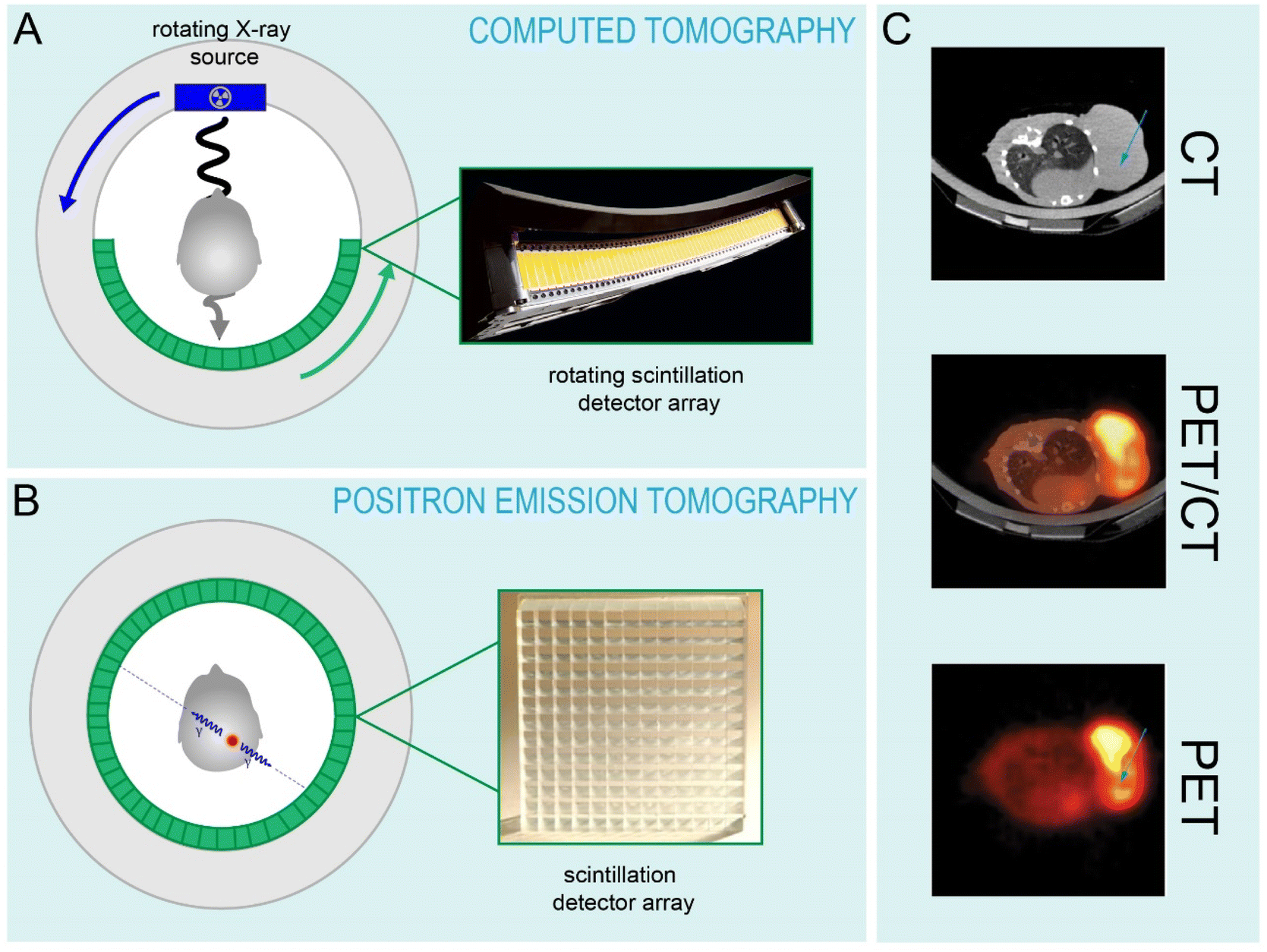 | ||
| Fig. 4 (A) Schematic of the principle of a computed tomography (CT) scanner. The rotating scintillation detector array shown is a GE Gemstone array. Detector photograph courtesy of GE. (B) Schematic of a positron emission tomography (PET) scanner. The scintillation detector array shown is a 13 × 13 LSO:Ce3+ array. Each scintillator crystal is 4 mm in diameter. (C) CT (top), PET (bottom) and combined PET/CT (middle) images of a mouse bearing a tumor. GE array. LSO detector array photographs and mouse imaging photographs modified from ref. 157. | ||
000 photons per MeV) and faster decay time (40 ns) than BGO. Similar crystals such as Gd2SiO5:Ce3+ (GSO) were also developed, but GSO has a significantly lower light yield (7600 photons per MeV) with a comparable decay time (60 ns). In the late 1990s, the first PET scanners employing LSO:Ce3+ (ECAT ACCEL, Siemens) and GSO:Ce3+ (Allegro, Philips Healthcare) were produced.130,164 Yet again, the allowed 5d → 4f transitions of Ce3+ that give rise to fast decay times facilitated important technological advancements. Specifically, the high light yield from Ce3+ in LSO allows for better spatial resolution, and the fast decay times of Ce3+ in LSO and in LYSO (containing a portion of Y3+ in place of Lu3+) have enabled time-of-flight (TOF) PET imaging, as the 40 ns decay times make it possible to correlate positron annihilation events with high temporal precision.119,165,166 Specialized PET scanners for positron emission mammography (PEM) are also made and rely on the use of these LYSO:Ce3+. The only commercially available PEM scanner, the NaviScan Flex Solo II™, utilizes LYSO:Ce3+ because it is imperative that minimal radiation doses are delivered to breast tissue during scanning, thus extremely fast imaging capabilities are required.167,168For nearly a decade, no single-modality PET scanners have been produced.164 Rather, there has been a transition to combined PET/CT imaging within a single gantry, as the anatomical information provided by CT provides greater information about the location of malignancies that are detected by PET (Fig. 4C). Unfortunately, the properties that make a scintillator favorable for use in PET or CT are not mutual, so a scintillator detector panel that can do both imaging modalities has not been yet achieved. The significant afterglow component in LSO:Ce3+ precludes its use as a CT detector, while the relatively slow decay times of Eu3+ and Pr3+ preclude their use in PET.169 Current generation TOF-PET/CT scanners like the Siemens BiographVision™ and Philips Gemini™ TF scanners employ LSO:Ce3+ and LYSO:Ce3+, respectively, for PET and GOS:Pr3+ (UFC™) for CT. State of the art clinically used TOF-PET/CT devices all employ lanthanide-based scintillators in one or both detector components, and are able to achieve temporal resolutions down to hundreds of picoseconds, which has enabled higher signal to noise and better spatial resolution, as well as quantitative dosimetry for radiotherapy treatment planning.131,164,169–171 Interestingly, GE announced in October 2022 a new generation of PET/CT scanners (Omni Legend) that utilize BGO crystals for the PET component, which is essentially full-circle in the PET detection field.172 In this case, it is not the efficiency of the scintillator, but the efficiency of the other detector components that enables the use of a lower light yield, slower scintillator crystal. Even in the case of the BiographVision™ 600, which uses LSO:Ce3+, the introduction of a SiPM detector array instead of PMTs enabled tremendous advancements in terms of scintillator-detector overlap and signal acquisition.171 Notably, the search for scintillators that can continue to advance these imaging modalities is at the forefront of the materials science field.131 However, the advancements that will be generated are likely to be in finding hosts that enable higher attenuation, higher light yields, better energy resolution and higher optical transparency, and that can be produced at high qualities at low cost. Combined, these advancements would enable lanthanide luminescence to be harnessed at maximum efficiency by the next generation of medical imaging detectors.
4.4 Electron microscopy
Electron microscopy also relies on the use of scintillator-based imaging and benefits from the same advancements made in medical imaging. In electron microscopy, it is often necessary to use rapid acquisition times, as samples can often degrade under the electron beam. Moreover, the image can be degraded by scattering if the phosphor screen used for viewing is too thick. For these reasons, scintillators with high light yields, high densities, fast decay times and minimal afterglow are desired. Early electron microscopy relied on visual inspection of the generated image, and green phosphors were desired owing to the sensitivity of the eye in the green spectral region.173 Tb3+ based phosphors became routinely used in the viewing screens for electron microscopy alongside other green phosphors such as ZnS:Cu. Today, GOS:Tb3+ is still commercially available for use in viewing screens, usually marketed under the common name P43.174 However, the long decay time of Tb3+ (1 ms) motivated researchers to use YAG:Ce3+, known as P46, which has an emission maximum at 530 nm and a decay time of 300 ns, with a much shorter afterglow component than GOS:Tb3+. When Tb3+ is added to P46, the P47 phosphor was developed, which has a blue emission but an even faster decay time at 100 ns.174 While the Ce3+-based viewing screens have much faster decay times, GOS:Tb3+ has a higher light yield, which allows for more sensitive detection. The first all-digital microscopes were also made possible by lanthanide scintillators, and employed YAG:Ce3+ coupled to fiber optics and bonded to CCD or CMOS detectors to generate images.175 In contrast to microcrystalline viewing screens for the detection of primary electrons, back-scattered electrons (BSE) and secondary electron detection require the use of single crystals. The small number of electrons detected by the annular detectors at high and low scattering angles make single crystal detectors the best option for providing the highest quality images with good contrast.176 Ce3+ garnet (YAP:Ce3+ and YAG:Ce3+) single crystals are employed in the REBEKA™ and KARMEN™ scanning electron microscope BSE detectors made by CRYTUR Ltd.177,178 In 2021, Gatan Inc. was granted a patent on microcrystalline Ce3+ and Pr3+ garnets for use in electron microscopy, suggesting there will be new imaging technologies based on scintillators with much faster decay times.179 As direct electron detectors become more commonplace, lanthanide-based technologies may likely remain as an alternative option.4.5 Astronomy
Scintillators also play an important role in astronomy, especially given that the cost-benefit consideration is far different from that in industry, as mentioned in the introduction. Highly specialized detectors are needed and are often custom designed for a specific application, mostly for various gamma and X-ray spectroscopy studies. Gamma ray spectroscopy is used in interplanetary space missions to study terrestrial and atmospheric compositions of planets, solar flares, and extra-galactic bodies such as black holes, stars and supernovas. X-ray spectroscopy is also used for those purposes, along with studies of hot gasses and objects falling into black holes. For both X-rays and gamma rays, it may be desirable to produce images, spectra to detect elemental signatures, or time-of-flight data to ascertain the location of a radiation source.180 Each of these goals requires scintillators with different properties, and most of them need to have fast decay times, high light yields and be of sufficiently high density to attenuate MeV and GeV photons. Especially with respect to extragalactic bodies, low photon fluxes from these distant sources mean highly sensitive detectors are a necessity. With respect to density, this can often mean the thickness of the scintillator (and consequently the weight) are of concern, as there is generally a desire to have instruments as compact as possible. NASA missions are currently using probes employing Ce3+-based scintillators like CLYC and CLLB (Glowbug181) and SrI2:Eu3+ (Strontium Iodide Radiation Instrumentation II (SIRI-2)182) for gamma-ray spectroscopy. The Gamma Ray Neutron Spectrometer (GRNS) aboard the Messenger Spacecraft that orbited Mercury for several years employed a Ce3+-doped 6Li glass to detect both gamma rays and neutrons in a similar manner as the Glowbug detector. The European Space Agency used GOS:Tb3+ supplied by Scintacor in the PROBA2 detector to image the solar corona via detection of high-energy UV photons.183,184 This is one of the few examples found where polycrystalline materials were used. Compton cameras/telescopes are also used to detect gamma rays but rely on the kinematics of Compton scattering to generate images. CeBr3 is used in NASA's Advanced Scintillator Compton Telescope (ASCOT),185 and LaBr3 was used for time of flight measurements of the FAst Compton TELescope (FACTEL).186 ASCOT is a successor to a previous mission called COMPTEL, which used NaI(Tl). The ASCOT CeBr3 had a time-of-flight resolution of 225 ps, while COMPTEL had a resolution of 1 ns, thus the use of CeBr3 provided a nearly four-fold improvement in resolution over its NaI(Tl)-based predecessor.180,185 Notably, the rest of the design was the same as the COMPTEL instrument and only the scintillator was changed. The Japanese Space Agency JAXA and NASA collaborated on the Astro E2 “Suzaku” satellite, upon which GSO:Ce3+ detectors were used in the hard X-ray detector, HXD-II, until 2015 when the satellite was decommissioned.187,188 The GSO:Ce3+ detectors were manufactured by Hitachi Chemical Co. and achieved energy resolutions better than that of the IBIS spectrometer aboard the ESA's INTEGRAL spacecraft, which used CsI detectors.188,189 Launched in 2017, the China Seismo Electromagnetic Satellite (CSES) is a collaboration between the Italian Space Agency and the Chinese Manned Space Agency that is monitoring the stability of the Van Allen radiation belts using LYSO:Ce3+-based detectors.190,191 LYSO:Ce3+ was chosen for its good energy resolution and ability to fully attenuate protons and electrons that are up to 250 MeV in energy. In most cases, lanthanide-based scintillators outperform the traditional BGO, CsI(Tl) and NaI(Tl) scintillators, and are the preferred materials when extremely high performance is desired and cost is not the prohibitive obstacle. The continued development of technologies used for astronomy experiments will almost certainly benefit from advancements made in materials science as well.5 Anti-counterfeiting
Recent estimates have suggested that approximately $500 billion USD of counterfeit or pirated goods are sold each year, accounting for over 2% of global trade.192 This number is only expected to rise with the increase in popularity of e-commerce and online shopping, making it more difficult to verify the validity of goods or products. The most prevalent industries affected by counterfeit goods include footwear and textiles, jewelry, electrical and medical equipment, and even pharmaceuticals.193 As a result, the distribution of counterfeit products not only impacts the economy but also has health implications, especially in developing nations, due to counterfeit antibiotics or other medication distributed in low-income countries.194 Therefore, industry manufacturers look to tag or label their products with characteristic and unique markers that distinguish them from counterfeits.Known as taggants, the unique labels that manufacturers rely on to identify their goods can assume many forms, including physical, chemical, or spectroscopic markers.195,196 The benefit of spectroscopic markers is that they're non-destructive, invisible, and highly versatile, due to the wide variety of possible excitation and emission wavelengths. They can either be fluorescent molecules or inorganic phosphors, although, some uncertainties in the chemical and photostability exist for the organic molecular taggants.197 Thus, many companies, contracted by industry to secure their goods, utilize phosphors as spectroscopic taggants. These phosphors often contain lanthanide ions, such as europium or cerium, due to their robust, characteristic, and bright emission spectra.
There are documented instances of lanthanide-doped phosphors used in anti-counterfeiting, though this list remains limited since agencies do not advertise the exact nature of their taggants. Companies that explicitly promote the use of lanthanides as the basis of their phosphors are therefore scarce. Among them, the HelioSUITE from Luminescence Sun Chemical Security advertises luminescent inks that can improve the security of banknotes and other government documents.198 Honeywell's Lumilux® exploits inorganic phosphors that can be embedded into plastic cases, fabrics or metals to help secure a variety of goods.199 This technology aims at markets that include healthcare, food products, as well as the automotive industry. Similarly, Olnica advertises rare-earth compounds that can be inserted in plastics and paper to make secure food packaging and security labels.200
Evidently, counterfeiting extends beyond private corporations, as government documents are also subject to forgery and imitation.201,202 Therefore, countries are required to invest heavily in security measures that prevent fraudulent documentation, and every nation does so differently. Some countries use lanthanide-doped phosphors as spectroscopic taggants embedded in banknotes and other documents. Under ultraviolet excitation, these luminescent features are observed on different currencies and passports from around the world, as presented in Fig. 5. While the exact identity of the different phosphors is intentionally unknown, speculating on their composition acts as a good exercise to showcase the practicality of incorporating lanthanide-doped phosphors to prevent counterfeiting.
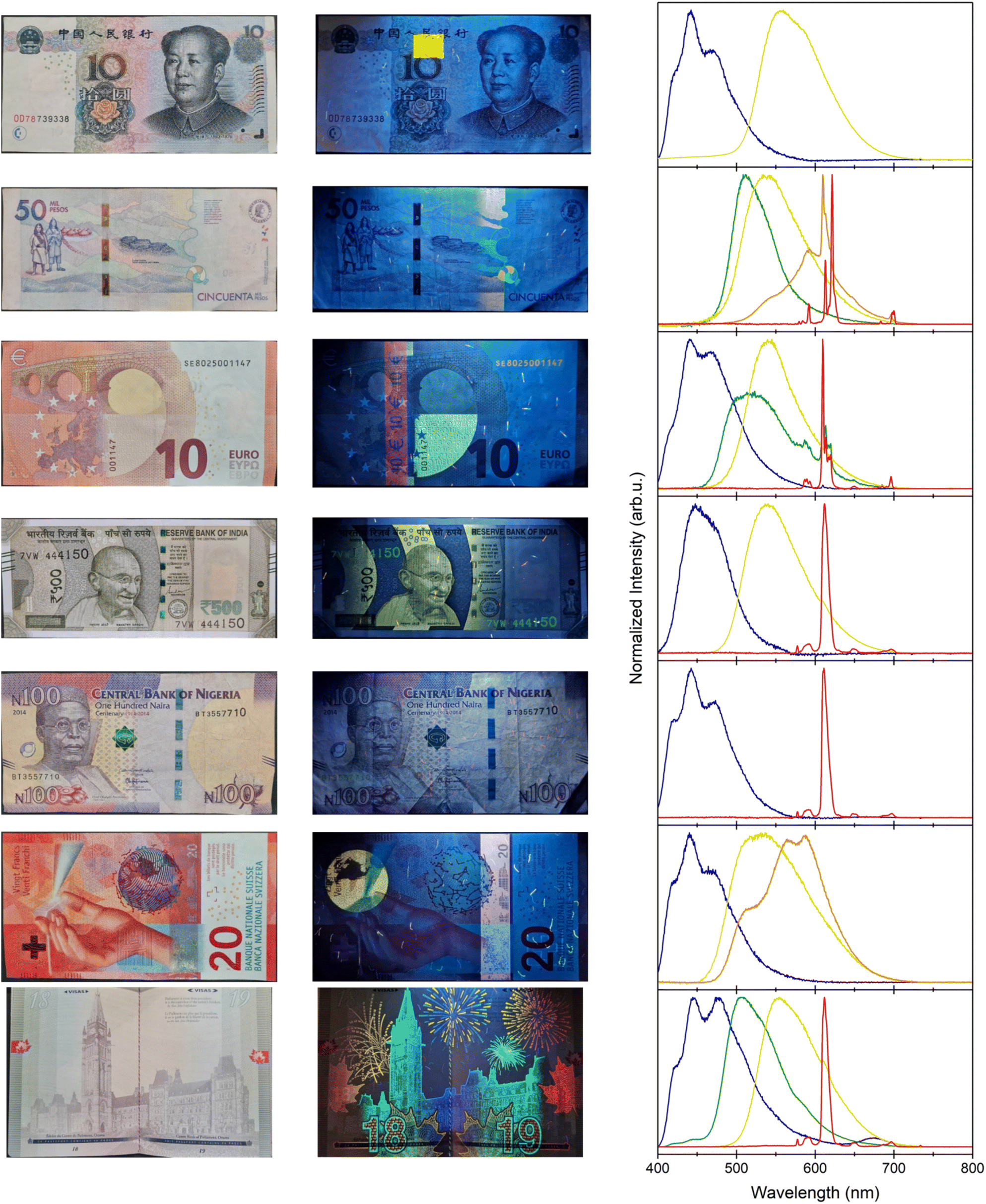 | ||
| Fig. 5 Banknotes and documents from several countries (Left) photographed under ambient lighting, (Center) photographed under UV lamp irradiation (λmax: 365 nm) and (Right) recorded emission spectra of the various observed phosphors. Chosen documents (from top to bottom) are 10 Chinese yuan, 50000 Colombian pesos, 10 euro, 500 Indian rupees, 100 Nigerian naira, 20 Swiss francs, and a visa page from the Canadian passport. | ||
The first anti-counterfeiting feature shown in each of the banknotes photographed in Fig. 5, under UV irradiation, is the presence of some luminescent dashes and speckles. A known technique in anti-counterfeiting is the physical unclonable function (PUF), in which a patterned tag is generated through a stochastic process and recorded ahead of distribution.203 By definition, each pattern is unique and non-reproducible. A recorded image is stored by the manufacturer and only shared with parties that need this key for authentication purposes. Regardless of the emission color, one feature on all banknotes that use spectroscopic taggants is a speckle pattern that is comprised of one or more phosphors, generating a PUF. In some instances, such as the euro, the fibers even alternate colors, forming a more complex feature. These luminescent fibers are randomly distributed across the entire banknote, making each one unique. If the banknotes are irradiated with ultraviolet light and photographed ahead of circulation, banks can cross-reference each note using its serial number to ensure its authenticity. By using multiple phosphors, the encryption can be made even more complex.204 One such limitation to this technique is the resolution of the stored photographs, where the number of photographed pixels increases the encoding capacity exponentially.
A second evident anti-counterfeiting measure is based on the uniqueness of the characteristic emission spectra of the chosen phosphors, as shown in the emission spectra of Fig. 5. For security purposes, the exact composition of the different phosphors is not publicized. However, it is evident that the narrow bands from the red-emitting features on all the analyzed banknotes and documents in Fig. 5 are characteristic of Eu3+. Because these transitions originate from the shielded electrons in the 4f orbitals of Eu3+, their band positions do not vary greatly with host. Whether this ion is coordinated to organic molecules or doped in an inorganic material, these bands are unique to the 5D0 → 7FJ transitions ranging between 575 and 750 nm.205,206 Rather, the observed splitting patterns can change depending on the Eu3+ environment. Previous reports on the identity of the red Eu3+ luminescence in the euro suggest that an 8-coordinated complex is used, containing three bidentate β-diketone moieties.207,208 A commonly studied ligand that results in a similar emission splitting pattern is 2-thenoyltrifluoroacetone (TTA), which can be paired with a variety of other ligands to fulfill the 8-fold coordination.209,210
The use of ligands to form complexes has some advantages. In comparison to other lanthanide 4f → 4f transitions, the Eu3+ emissions from the 5D0 excited state are some of the most efficient, with quantum yields typically around 50%.211,212 This is important as the more efficient a phosphor or luminescent species, the less of it is required in a spectroscopic taggant, which minimizes the cost. Nevertheless, Eu3+ and the other lanthanides have weak absorption cross-sections, which are magnitudes lower than fluorescent organic molecules. The use of spectroscopically active ligands, such as TTA, overcomes this issue by absorbing the incident ultraviolet light and transferring the energy to the Eu3+ metal center non-radiatively via the antenna effect.213–216 This results in efficient luminescent complexes exploited for their bright red emissions.
Interestingly, these Eu3+ complexes are quite versatile. While the splitting patterns of the Eu3+ 5D0 emissions between the euro and the other red-emitting documents are very different, the peak positions match perfectly with the Indian rupee, the Nigerian naira, and the Canadian passport. When Eu3+(TTA) complexes are electrospun into polymer fibers, such as poly(vinyl pyrrolidone), the environment surrounding the Eu3+ ions changes.217–219 This results in the observed differences in the red emission spectra of Fig. 5, where the discrete band splitting broadens. The 5D0 → 7F0 emission at 578 nm also appears, which is indicative of a low symmetry environment not present in the native complex.205 The incorporation of these complexes within a polymer matrix improves its thermal and photostability, which is of utmost importance to the longevity of the security feature in something as manhandled as banknotes.
In contrast to the Eu3+ complexes, the Colombian peso elects to use a different red emitter entirely. The splitting pattern is reminiscent of an oxysulfide composition, such as Y2O2S or Gd2O2S.220,221 When doped with Eu3+, these materials are commonly used in lighting applications, such as cathode ray tubes and imaging detectors as discussed above.222–224 Eu2+-doped oxysulfide compositions are extremely photostable, which is why their widespread use in a variety of different industrial phosphor applications is so common.
All the documents recorded herein incorporate a similar blue luminescent phosphor, with distinct but overlapping emission bands. Previous reports have alluded to a (BaO)x·6Al2O3 material doped with 2 to 15 mol% Eu2+.207,208 When x = 0.82, the phosphor has an emission maximum at 440 nm, and other values of x slightly shift the emission band.225 Therefore it was speculated that the industrial synthesis of this phosphor results in phase-impure particles, resulting in a primary band at 440 nm that overlaps with a more broad band spanning from 410 to 525 nm. Through the use of Eu2+, the allowed 5d → 4f transitions vary with the host, and facilitate a favorable emission in the blue region when doped into aluminate or silicate materials.226 These oxide-based materials are common in lighting applications (Section 2), owing to their quantum yields that can exceed 70%.227,228
The recorded green and yellow phosphors are more difficult to determine since the emission spectra do not have any defining features. The choice of inorganic phosphor that may be responsible for such emissions can only be speculated as a potential option. A likely candidate that has previously been suspected of being in the euro is SrGa2S4:Eu2+.207 This material has multiple sites for the Eu2+ ion, creating a broadband emission centered in the green region of light with emission intensities similar to common phosphor materials in lighting applications.229–232 A commonly used yellow phosphor in lighting applications is Ce3+-doped Y3Al5O12 (YAG), with an emission spectrum ranging from 500 to 650 nm, and quantum yields that exceed 80%.233–235 Therefore, it is not too farfetched to consider these materials as likely candidates for the green and yellow features, respectively, present in the recorded documents.
Contrarily, the orange phosphors have many overlapping features and emission maxima, making them equally difficult to determine. For example, the iconic Cittarium pica on the Colombian peso consists of some characteristic Eu3+ signals, but in a different composition from what was discussed previously, overlapping a broader emission band spanning 500–700 nm.236 Similarly, the globe feature on the Swiss franc contains multiple emission maxima between 475 and 700 nm. These bands can possibly, but not unequivocally, be attributed to materials co-doped with Mn2+ and Eu2+, which possess similar emission spectra when doped into phosphates.237–239
It is interesting to observe the wide variety of colors that exist in different documents as a means of anti-counterfeiting, with many different lanthanide complexes and phosphors available. When weaved into the paper fibers, these banknotes and documents become exceedingly difficult to replicate. Only with specialized equipment and expertise is it even possible to observe, let alone reproduce, such complicated security measures. When corroborated with other features, such as the aforementioned serial number and PUFs, or even non-luminescent features, it becomes clear how determined governments and private industry manufacturers are to prevent forging, and how willingly they invest heavily with the purpose of limiting counterfeiting.
6 Telecommunications
As technology has developed over the last century, the internet and other means of communicating information across the globe has advanced at a commensurate rate. Historically, copper wires pulsing an electric current conveyed information in the form of binary sequences. However, the development of optical fibers in the 1970s by Corning researchers Donald Keck, Robert Maurer, and Peter Schultz revolutionized the method through which data is communicated.240,241 By exploiting pulses of light instead of electric currents, today's telecommunications technology can be transferred over larger distances with greater speed, less signal loss, larger bandwidths, and are designed more practically for industrial use (Fig. 6).242–244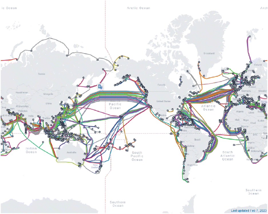 | ||
| Fig. 6 Map of the submarine telecommunications cables around the world as of 2023. Reproduced from https://www.submarinecablemap.com/. | ||
Optical fibers exploit the use of high-purity fused silica for light propagation.245 The core is composed of fused silica doped with an impurity such as germanium dioxide or chlorine, to increase the refractive index which achieves total internal reflection.246 Semiconductor diode lasers act as the light source in optical signals because of their compact size and range of potential wavelengths.247 The choice of wavelengths used in optical telecommunication is dependent on the absorption coefficient of the fused silica, which is lowest in the near-infrared (NIR) region. Ranging from 1260 to 1625 nm, the attenuation of light through the optical fiber materials is less than 0.5 dB km−1, which is very important for long-distance data transfer.247 Within this range, two bands are the most widely used, the O-band between 1260 and 1360 nm, and the C-band between 1530 and 1565 nm.248 While the O-band has higher attenuation in fused silica, the C-band is subject to greater chromatic dispersion, which distorts and can possibly overlap pulses of the incoming signal. Therefore, the O-band is specifically used in shorter-distance information transfer, while the C-band is exploited in long and ultra-long haul telecommunication applications.
Despite these advancements in the transmission of information, light signals confined to the inside of optical fibers are still subject to losses over distances that exceed 100 km.249 Amplifiers overcome this dilemma by periodically increasing the signal intensity, improving data transfer from the transmitter to the receiver. Traditional amplification involved the conversion of light signals to electric current that could then be amplified before converting back to light.250 This process was impractical and slow, acting as a bottleneck that greatly limited transfer speeds. The use of lanthanides in optical amplifiers was introduced in the late 1980s as a faster alternative.249 Given the abundance of potential energy levels in trivalent lanthanides, the study and use of fiber amplifiers have included ions of neodymium, praseodymium, holmium, erbium, thulium, and ytterbium, which all have excitation and emission bands in the NIR region of light.251–256 Following the basic premise of a laser, lanthanide ions doped into an optical fiber could be excited using an external laser source (separate from the telecommunication signal).257 The long-lived excited states help facilitate population inversion, and the incoming photons from the information signal induce a stimulated emission. This stimulated emission results in more photons that are in-phase and monochromatic with the telecommunication signal, and since the signal does not need to be converted to an electric current, faster amplification is achieved.
First discovered in 1987, the erbium-doped fiber amplifier (EDFA), which consists of fused silica fibers doped with Er2O3, is still the most commonly used optical signal amplifier today.258 EDFAs increase the signal intensity of data transmissions operating in the C-band, due to the efficient 4I13/2 → 4I15/2 emission of Er3+ at 1550 nm.259–261 When excited using a 980 nm laser, the Er3+ ions are promoted into the 4I11/2 excited state. This ion then relaxes non-radiatively to populate the 4I13/2 level. When the excitation source is of sufficiently high energy, there is an accumulation of Er3+ ions excited into this state, achieving the necessary population inversion to properly amplify the subsequent data signals. Once a data signal (with a wavelength of approximately 1550 nm) interacts with the excited Er3+, the ion relaxes to the ground state, ejecting an electron in-phase with the original optical signal. High-power amplifiers use 1480 nm as the Er3+ excitation source instead (populating a sublevel of the 4I13/2 state).259,262 This excitation wavelength has a lower absorption cross-section than 980 nm, but under certain conditions can outperform the amplification capabilities from 980 nm excitation.
When data transfer is not required to travel extended distances (<100 km), the O-band is preferred, with wavelengths around 1300 nm, which are not as susceptible to chromatic dispersion compared to the C-band.248 Praseodymium-doped fiber amplifiers (PDFAs) based on silica or fluoride compounds are used as signal amplifiers instead, owing to the resonance in this wavelength region.263–265 Similar to EDFAs, the Pr3+ ions are excited into the 1G4 state using an external ≈1000 nm laser source. Incoming signal photons of 1300 nm can then induce stimulated emission of the 1G4 → 3H5 transition, amplifying the signal. Interestingly, the energy levels of Pr3+ help facilitate population inversion, more so than Er3+, since the 1300 nm emission does not relax the ions to the 3H4 ground state, which follows the premise of a four-level laser.266 However, the quantum efficiency of the 1G4 → 3H5 transition is low, as compared to Er3+, due to multiphonon relaxation processes that quench the 1G4 excited state to lower-lying states. These intermediate states are not present below the emitting 4I13/2 level of Er3+ (Fig. 7). These subtle differences in EDFAs and PDFAs influence the way they are engineered to overcome their respective shortcomings.
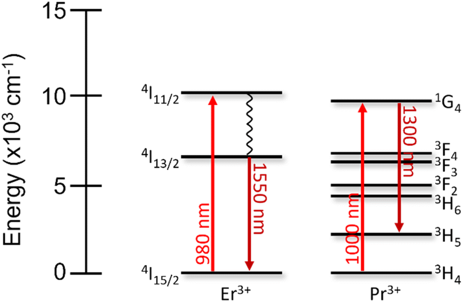 | ||
| Fig. 7 Energy level diagrams of Er3+ and Pr3+ depicting the excitation and emission wavelengths relevant for their use in optical amplifiers. | ||
As the demand for faster telecommunication speeds increases, recent studies aim to further advance the way optical information signals are transmitted. One such advancement is the use of polymeric optical fibers instead of the traditional fused silica.267,268 Polymeric fibers are less expensive to manufacture, lighter, and more flexible than silica.269 However, since phonon quenching is a common drawback to lanthanide luminescence, the abundance of O–H, N–H, and C–H vibrations that are present in polymer materials hinder their effectiveness as optical amplifiers. Moreover, the approach to incorporating lanthanides in polymers must also be modified, since inorganic oxides will not be suitable. Lanthanide complexes with fluorinated ligands have emerged as the preferred option, owing to weaker vibrational modes from C–F bonds rather than C–H bonds.270,271 However this technology is still in its infancy, since the signal amplification is still not sufficient to compare with traditional EDFAs.
Newly emerging erbium-doped waveguide amplifiers (EDWAs) are showing promise in advancing signal amplification in optoelectronics.272 These devices consist of lanthanide complexes embedded within silica and polymers on a silicon substrate.267,273 Following the same optical amplification technology as EDFAs, EDWAs are directly manufactured into integrated circuit boards, avoiding the need for external signal amplification. As our reliance on global communication increases, it will likely become necessary to develop materials which are capable of transmitting data of even larger sizes at even faster rates. Likely, lanthanides will continue to aid in facilitating the next generation of telecommunication technologies.
7 Next-generation technologies
7.1 Solar energy conversion
Currently, the spectral mismatch between the materials used in solar cells and the solar emission spectrum represents a major obstacle to increasing the efficiency of existing photovoltaic (PV) cells (Fig. 8).274 For example, the maximum absorption by silicon PV cells is only 48% of the total solar emission, since they absorb in the range of approximately 400–1200 nm, whereas the entire solar emission spectrum ranges approximately 250–2500 nm. Moreover, the most efficient conversion of solar energy to electricity occurs when the semiconductor absorbs light at wavelengths closest to its intrinsic bandgap. Thus, silicon, GaAs and halide perovskite PVs are most efficient around 900–1100 nm but can also less-efficiently absorb visible light.275–277 Lanthanide-based spectral wavelength converting technology has the potential to expand our ability to harness additional wavelengths from the solar spectrum.274–276 In this way, lanthanides are mostly used in complementary technologies or in direct combination with silicon PV devices, since those are already well-established in the commercial market. Less commonly, lanthanides incorporated into the semiconductor components of PV cells are also under investigation and have been patented.278,279 Organic polymers and dyes represent the main alternative to lanthanides in the solar industry and are substantially less expensive. However, the photostability of lanthanide-based materials represents an important advantage that may justify the added cost of their use.275,276,280,281 At this time, widespread commercial use of lanthanide luminescence in solar energy conversion has not been realized. However, there are many active patents toward the development of such technologies, and we aim to focus this discussion on conclusions we can base on the research that has made it to the patent stage. The interested reader is directed to several publications that provide an in-depth discussion on the state of the field based on academic literature.274–276,278,282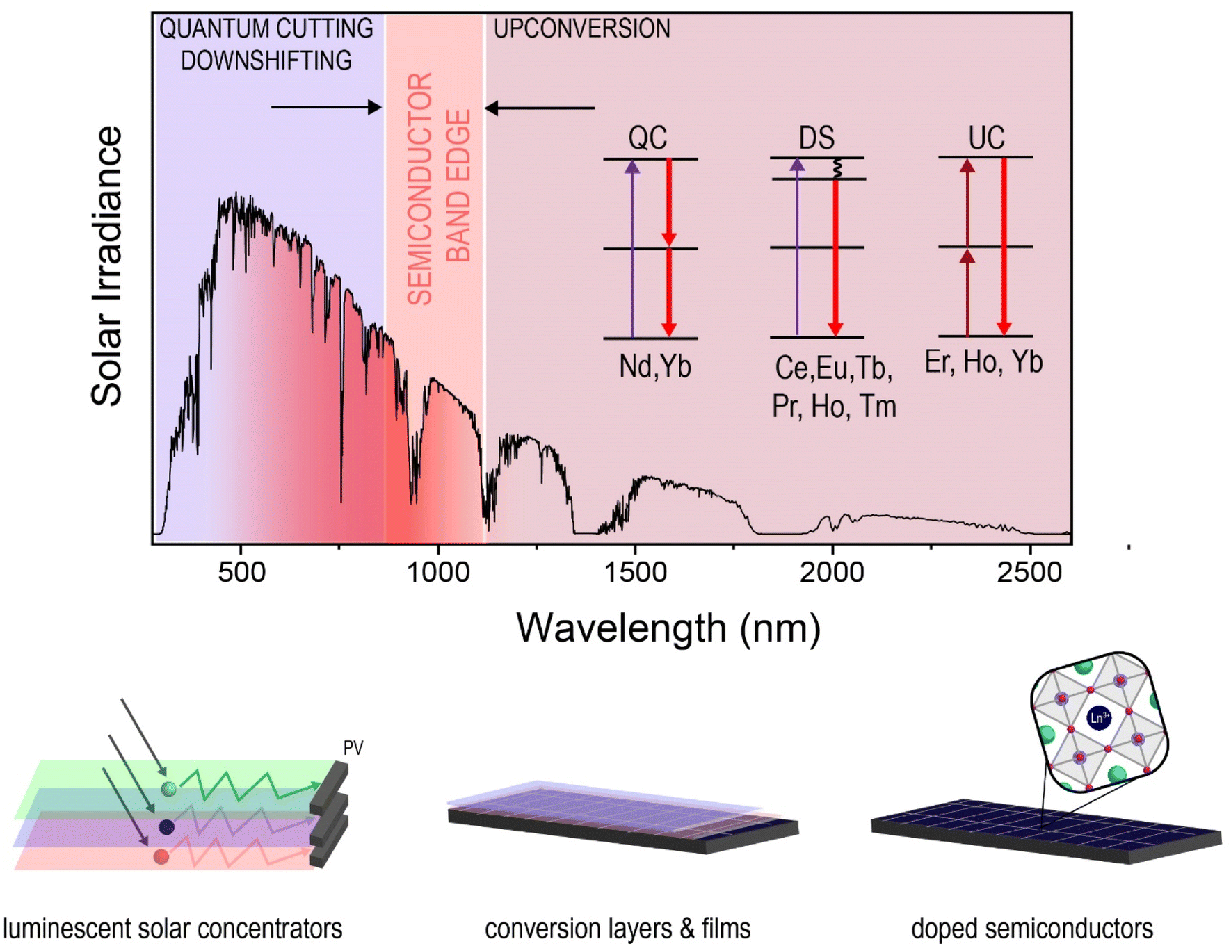 | ||
| Fig. 8 Solar energy conversion technologies using lanthanides. The solar irradiance spectrum (top) and corresponding regions of wavelengths where upconversion, quantum cutting and downshifting can be harnessed. Inset shows the mechanisms relevant to each of the luminescence mechanisms. On the bottom, there are graphical depictions of luminescent solar concentrators (left), photovoltaic conversion layers and films (middle) and photovoltaic cells doped with lanthanides directly into the semiconductor layer. | ||
Lanthanides can absorb solar wavelengths otherwise not absorbed by the PV cells, and re-emit them at longer or shorter wavelengths, through quantum cutting (QC)/downshifting (DS) or upconversion (UC) processes, respectively (Fig. 8).274,283 These newly emitted photons can then be absorbed by the PV cells, improving their solar harnessing capabilities. The process of upconversion involves the absorption of two or more low energy photons which are converted into a higher-energy photon. In this way, NIR light that is lower than the bandgap energy of the PV semiconductor (>1100 nm in the case of silicon) can be harnessed and converted to wavelengths suitable for bandgap excitation. On the contrary, in QC/DS, a higher-energy photon is converted into one or more low energy photons.6 In this way, the UV and visible wavelengths are harnessed and converted to longer wavelengths. The characteristic narrow emission bands from the 4f → 4f transitions of Ln3+ ions fulfill the requirements for the conversion of the broad solar spectrum to a narrow emission range at wavelengths suitable for commercial PVs.
First patented by Renata Reisfeld in 1979, lanthanide-based luminescent solar concentrators (LSC) work by absorbing solar energy over a large surface area, transforming it into a fluorescent emission, and then focusing the light onto a smaller target which is then harnessed by PVs at the edge of the LSC.276,284 LSCs are usually transparent and can be multilayered to achieve the use of a wider range of the solar spectrum by incorporating different lanthanides into different layers.277,284,285 This type of technology is particularly interesting for urban applications where LSCs can be incorporated into building architecture, especially in windows since LSCs require large surface areas to operate.276 In a similar fashion, many patented technologies use transparent lanthanide films as layers directly on PV surfaces.286–289 In both technologies, specific lanthanides are more successful either for UC or QC/DS; the main difference is simply whether the lanthanide components are used in tandem with a PV cell or directly coated onto one.
NIR light is harvested and transformed to useable wavelengths via UC, with most technologies using Er3+ or Er3+ and Yb3+ together. In this way, Er3+ can absorb wavelengths around 1550 nm, and emit at 980 nm upon sequential absorption, which is close to the band edge of silicon. Similarly, both Er3+ and Yb3+ can absorb 980 nm photons, resulting in the emission of green light from Er3+ that is well-absorbed by GaAs PVs. Several layered PV designs are under active patents using Er3+ and Er3+/Yb3+.288,290,291 These ions are also well-established in the literature and appear to be the optimal choices for harnessing NIR light in PV devices.274–276 To our knowledge, there are few active patents involving lanthanide-based layers as upconversion layers in LSCs, and they also use Er3+ and/or Yb3+.277,285
Upconversion is substantially more limited in efficiency than QC/DS, as expected from an anti-Stokes process. For this reason, there are substantially more examples of lanthanides as QC/DS converters. Eu3+ is perhaps the most well-established for solar QC/DS, taking advantage of UV light, since its red emissions are closer to the desired wavelengths, and some Eu3+ complexes have particularly impressive quantum efficiencies relative to other lanthanides.275,287,292 In many cases, the antenna effect is particularly useful, in which the ligand (having a higher absorption cross-section than the lanthanides) absorbs the incident solar light and transfers it to the lanthanide metal center.277,287,292 Tb3+ complexes are the second-most promising for QC/DS, as they also efficiently absorb UV light, but convert it to green light, which is somewhat less desirable for use with a silicon solar cell but is still efficient for the excitation of GaAs PVs.284 Notably, the luminescence of Tb3+ and Eu3+ complexes was reported to be significantly enhanced by noble metal nanoparticles due to plasmon resonance.274,276,277 Nd3+-Yb3+ complexes are also able to harvest blue light and convert it to NIR via QC at 980 nm, even closer to the intrinsic bandgap of silicon than the Eu3+ emissions.293 The QC process occurs via energy transfer from Nd3+ to Yb3+, following the mechanism [Nd3+ (4G9/2 → 4F3/2); Yb3+ (2F5/2 ← 2F7/2)], followed by a second energy transfer from the Nd3+(4F3/2) level to the Yb3+(2F5/2) level, yielding two NIR photons from Yb3+. In theory, QC is particularly attractive because of the potential to achieve quantum efficiencies greater than 100%.275 In practice, the efficiencies are closer to a one-to-one process like DS. Ce3+ complexes are also proposed for their incorporation in LSCs in combination with other lanthanides such as Eu3+ and Tb3+, whereby Ce3+ can absorb UV light and energy transfer to the Eu3+ and Tb3+ complexes which then emit at more appropriate wavelengths.277 In some instances, the radiative 5d → 4f transitions of Ce3+ can be found in the green region, and thus Ce3+ can be directly used as a wavelength-converting ion. This has been proposed with YAG:Ce3+, as well as with Ce3+-doped perovskite quantum dots.294,295 PV devices based on halide perovskites have become quite attractive and are likely to be explored further for commercial translation. Notably, lanthanide-doped perovskite solar cells have gained momentum since 2015, reaching solar cell efficiencies around 20%.275,278 Most of the perovskite PV devices also employ Eu3+, Er3+, and Yb3+, though nearly all lanthanides have been assessed for incorporation into perovskite lattices or in films on top of a perovskite active layer.
Lanthanide-based solar technologies have been under development for nearly half a century, but have not yet reached widespread commercial adaptation.292 Advancements in improving the efficiencies of these materials are continually sparking new developments in the technologies making use of lanthanides, and suggest that there is still great potential for them in the commercial market. The photostability of lanthanide materials and the narrow emission bands from the 4f → 4f transitions of these ions are strong advantages over alternative technologies employing strictly organic molecules. Likely, hybrid organic-inorganic technologies will pave the way for commercial adaptations of lanthanide luminescence in the solar industry.286 If cost-efficiency barriers are adequately addressed, lanthanides will likely progress our abilities to efficiently harness the UV and infrared regions of the solar spectrum. However, this is a prime example of how cost-benefit evaluations are crucial for the introduction of an invention, no matter how promising it is.
7.2 Alternative lighting technologies
The application of lanthanide-based phosphors can provide benefits in several other industrial sectors. For military and space applications, the challenge to obtain produce in space is contingent on finding the right lighting system.296 Several kinds of crops and vegetables have been exposed to light with a different spectral distribution to verify the best growth conditions.297–299 Well-established products, such as white-light lightbulbs (as discussed in Section 2) that mimic the spectral characteristics of the sun for plant growth indoors, are also promising for farming in space. Obtaining a self-sustained ecosystem to support life in space is a recurring idea in recent years, which can potentially bring more lanthanides to outer space.Finally, the possibility to achieve lighting without additional energy consumption with persistent luminescence is quite attractive, but still far from being realized. Finally, the phenomenon of persistent luminescence should also be considered in view of its usefulness for safety signals and panels.27 In a material with an intermediate trapping state positioned appropriately within a band gap, the trap state can accumulate trapped charges during irradiation of the considered persistent luminescent phosphor. When irradiation ceases, the charges are released, producing persistent luminescence (also known as afterglow). The most efficient of these phosphors are Sr2MgSi2O7:Eu2+,Dy3+ (blue), SrAl2O4:Eu2+,Dy3+ (green) and Y2O2S:Eu3+,Mg2+,Ti (red).27 Persistent phosphors have found commercial use in everything from watch dials and glow-in-the-dark toys to emergency safety signage on buildings, passenger trains, and naval ships among others.300–303 Notably, SrAl2O4:Eu2+,Dy3+ signs have been used to replace radioactive tritium signs at military stations, thereby improving the safety of personnel.303 With respect to persistent luminescence duration, major optimizations have already been realized, achieving emissions that exceed 12 h. This certainly suffices in terms of replacing lighting in the absence of the sun (i.e. at night). However, the intensity of the emissions, and their color, require substantial improvements. Sunlight-activated persistent luminescent phosphors are nevertheless appearing in the literature, making them a foreseeable perspective for the future of lighting.304 Given that most of the modern persistent luminescent material advancements were made starting in the 1990s,305,306 the field is relatively young and thus there is still much to be learned towards making this a feasible lighting technology.
8 Conclusions
Lanthanide luminescence is ubiquitous in modern society, from under the oceans to deep space, since they have facilitated an incredible variety of technologies. Despite the difficulties faced in isolating and identifying these elements, as well as the uncertainties faced in their supplies, the modern world has become reliant on the lanthanides.The unparalleled narrow band emissions of the trivalent lanthanides have facilitated lighting and displays with high color purity and have allowed for the precise conversion of broad solar wavelengths to specific and useful emissions that can be harnessed by semiconductors in photovoltaic cells. Simultaneously, the broad 5d → 4f transitions have vastly improved the phosphor and scintillator industries.
With regard to the medical industry, the luminescent properties of the lanthanides have been crucial in everything from laser ablation in ophthalmologic surgery, to tattoo removal, to medical imaging in X-ray, PET and CT scanning. Moreover, their use in solid-state lasers has enabled wireless communications, facilitating the possibility for deep space communication and allowed us to monitor the atmosphere of the earth via LIDAR technologies from space. Lanthanides are also integrated in our everyday lives in the form of luminescence-based anti-counterfeiting in money and passports. The phosphors employed throughout these applications, incorporating the lanthanides as a dopant or part of the native composition, are summarized in Fig. 9, depicting their range as well as their versatility.
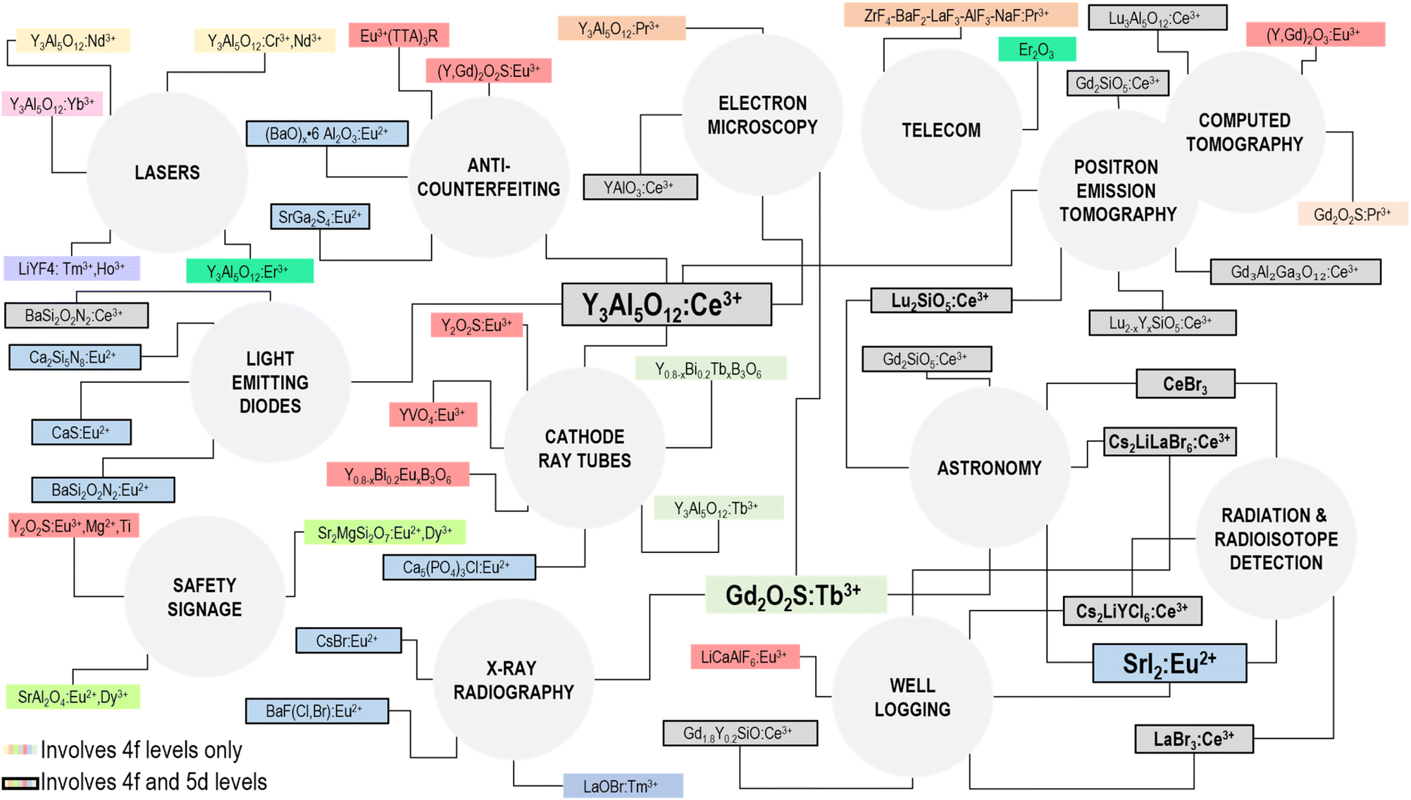 | ||
| Fig. 9 Summary scheme depicting the phosphors and materials mentioned throughout this review. | ||
As advancements are made in mining technologies, and more countries introduce rare-earth mining operations, the potential for stable supplies of lanthanides, as well as a decrease in their cost may occur. Notably, the lanthanides are not only prized for their luminescence properties, thus there are many additional reasons they are coveted. Solving these issues will likely spur the industry into taking advantage of the unique properties of these elements. Throughout this review, we aimed to provide an overview of how lanthanide luminescence has benefitted society, so that their historical uses and their use in today's technologies may inspire future researchers to harness lanthanide luminescence in the next generation of the modern era.
Author contributions
G. T. and G. A. M. contributed equally. All authors curated the references and wrote and edited the manuscript.Conflicts of interest
There are no conflicts of interest to declare.Acknowledgements
J. A. C. is a Concordia University Research Chair in Nanoscience and is grateful to Concordia University for financial support. J. A. C. is grateful to the Natural Science and Engineering Research Council (NSERC) of Canada for the sustained support of his research (No. RGPIN-2022-04704). G. T. is grateful to the Université Laval for financial support. S. L. M. and G. A. M. are grateful to NSERC for financial support through the Alexander Graham Bell graduate scholarships. S. L. M. is grateful for financial support from Concordia University's doctoral incentive fellowship. M. K. is grateful to Concordia University for financial support through the Tuition Award of Excellence.References
- E. F. Worden, R. W. Solarz, J. A. Paisner and J. G. Conway, J. Opt. Soc. Am., 1978, 68, 52–61 CrossRef CAS.
- F. J. Gustafson and J. C. Wright, Anal. Chem., 1979, 51, 1762–1774 CrossRef CAS.
- J. C. Wright, Anal. Chem., 1977, 49, 1690–1702 CrossRef CAS.
- L. Tansjö, in Episodes from the History of the Rare Earth Elements, ed. C. H. Evans, Springer Netherlands, Dordrecht, 1996, vol. 15, pp. 37–54 Search PubMed.
- Section 14: Geophysics, Astronomy and Acoustics, ed. J. R. Rumble, CRC Press/Taylor & Francis, 2022 Search PubMed.
- R. Eggert, C. Wadia, C. Anderson, D. Bauer, F. Fields, L. Meinert and P. Taylor, Annu. Rev. Environ. Resour., 2016, 41, 199–222 CrossRef.
- J. G. Bünzli, Eur. J. Inorg. Chem., 2017, 5058–5063 CrossRef.
- D. N. Woodruff, R. E. P. Winpenny and R. A. Layfield, Chem. Rev., 2013, 113, 5110–5148 CrossRef CAS PubMed.
- J. A. Cotruvo, ACS Cent. Sci., 2019, 5, 1496–1506 CrossRef CAS PubMed.
- J. C. G. Bünzli and C. Piguet, Chem. Soc. Rev., 2005, 34, 1048–1077 RSC.
- M. Shibasaki and N. Yoshikawa, Chem. Rev., 2002, 102, 2187–2209 CrossRef CAS PubMed.
- R. T. Wegh, H. Donker, K. D. Oskam and A. Meijerink, Science, 1999, 283, 663–666 CrossRef CAS.
- T. Senden, F. T. Rabouw and A. Meijerink, ACS Nano, 2015, 9, 1801–1808 CrossRef CAS PubMed.
- C. Ronda, J. Lumin., 2002, 100, 301–305 CrossRef CAS.
- C. Ronda, Prog. Electromagn. Res., 2014, 147, 81–93 CrossRef.
- United States Patent Office, US Pat.US234345A, 1880 Search PubMed.
- C. J. Cleveland and C. G. Morris, Handbook of Energy. Volume II_ Chronologies, Top Ten Lists, and Word Clouds, Elsevier, 2014 Search PubMed.
- F. Hauksbee, Philos. Trans. R. Soc. London, 1705, 24, 2129–2135 CrossRef.
- R.-S. Liu and X.-J. Wang, Phosphor Handbook, CRC Press, Boca Raton, 2021 Search PubMed.
- United States Patent Office, US Pat.US2182732A, 1927 Search PubMed.
- L. Ozawa and M. Itoh, Chem. Rev., 2003, 103, 3835–3855 CrossRef CAS.
- A. K. Levine and F. C. Palilla, Appl. Phys. Lett., 1964, 5, 118–120 CrossRef CAS.
- J. R. McCOLL and F. C. Palilla, in Industrial Applications of Rare Earth Elements, American Chemical Society, 1981, pp. 177–193 Search PubMed.
- United States Patent Office, US Pat.US2748303A, 1949 Search PubMed.
- United States Patent Office, US Pat.US3440080A, 1969 Search PubMed.
- United States Patent Office, US Pat.US3418246A, 1968 Search PubMed.
- United States Patent Office, US Pat.US3394084A, 1968 Search PubMed.
- United States Patent Office, US Pat.US3989977A, 1976 Search PubMed.
- Y. Gao, P. Jiang, W. Gao, R. Cong and T. Yang, J. Solid State Chem., 2019, 278, 120915 CrossRef CAS.
- N. Katoh, T. Deguchi and R. S. Berns, Opt. Rev., 2001, 8, 305–314 CrossRef.
- J. Ballato, J. S. Lewis III and P. Holloway, MRS Bull., 1999, 51–56 CrossRef CAS.
- Thomas Electronics, 2023, https://www.thomaselectronics.com/avionics/head-up-display/, accessed June 5 2023.
- C. Ronda and A. Srivastava, Electrochem. Soc. Interface, 2006, 15, 55–57 CrossRef CAS.
- R. Marin and D. Jaque, Chem. Rev., 2021, 121, 1425–1462 CrossRef CAS PubMed.
- A. Tiwari and S. J. Dhoble, Luminescence, 2020, 35, 4–33 CrossRef CAS PubMed.
- S. Jin, R. Li, H. Huang, N. Jiang, J. Lin, S. Wang, Y. Zheng, X. Chen and D. Chen, Light Sci. Appl., 2022, 111, 1–13 Search PubMed.
- United States Patent Office, US Pat.US3819974A, 1973 Search PubMed.
- Z. Xia and Q. Liu, Prog. Mater. Sci., 2016, 84, 59–117 CrossRef CAS.
- United States Patent Office, US Pat.US8597543B2, 2012, 347 Search PubMed.
- United States Patent Office, US Pat.US9530944B2, 2015 Search PubMed.
- United States Patent Office, US Pat.US7352006B2, 2004 Search PubMed.
- European Patent Office, EP1837386B1, 2005.
- United States Patent Office, US Pat.US7250715B2, 2004 Search PubMed.
- United States Patent Office, US Pat.US7951308B2, Partial English Transl. Off. Action issued Sep, 2010, vol. 29, p. 624 Search PubMed.
- A. Dunselman, Lighting world first: Philips breaks 200 lumens per watt barrier, 2013 Search PubMed.
- M. Richi, Success in research: First gallium-nitride LED chips on silicon in pilot stage, Munich. Germany, 2012 Search PubMed.
- M. Kawa and J. M. J. Fréchet, Chem. Mater., 1998, 10, 286–296 CrossRef CAS.
- M. Kaur, G. A. Mandl, S. L. Maurizio, G. Tessitore and J. A. Capobianco, Nanoscale Adv., 2022, 4, 608–618 RSC.
- M. Pietraszkiewicz, M. MacIejczyk, I. D. W. Samuel and S. Zhang, J. Mater. Chem. C, 2013, 1, 8028–8032 RSC.
- G. L. Law, K. L. Wong, H. L. Tam, K. W. Cheah and W. T. Wong, Inorg. Chem., 2009, 48, 10492–10494 CrossRef CAS PubMed.
- J. H. S. K. Monteiro and A. De Bettencourt-Dias, Lanthanide-Based Multifunct. Mater. From OLEDs to SIMs, 2018, pp. 99–131 Search PubMed.
- J. M. Ha, S. H. Hur, A. Pathak, J. E. Jeong and H. Y. Woo, NPG Asia Mater., 2021, 13, 1–36 CrossRef.
- L. Wang, Z. Zhao, C. Wei, H. Wei, Z. Liu, Z. Bian and C. Huang, Adv. Opt. Mater., 2019, 7, 1801256 CrossRef.
- A. De Bettencourt-Dias, Dalton Trans., 2007, 2229–2241 RSC.
- United States Patent Office, US Pat.US04168012, 1962 Search PubMed.
- F. Jobin, P. Paradis, Y. O. Aydin, T. Boilard, V. Fortin, J.-C. Gauthier, M. Lemieux-Tanguay, S. Magnan-Saucier, L.-C. Michaud, S. Mondor, L.-P. Pleau, L. Talbot, M. Bernier and R. Vallée, Opt. Express, 2022, 30, 8615 CrossRef CAS PubMed.
- A. A. Kaminskii, Phys. Status Solidi, 1985, 87, 11–57 CrossRef CAS.
- B. M. Walsh, N. P. Barnes, M. Petros, J. Yu and U. N. Singh, J. Appl. Phys., 2004, 95, 3255–3271 CrossRef CAS.
- D. W. Ball, Field Guide to Spectroscopy, SPIE Press, Bellingham, 2006 Search PubMed.
- United States Patent Office, US Pat.US3252103A, 1964 Search PubMed.
- U. Keller, Nature, 2003, 424, 831–838 CrossRef CAS PubMed.
- United States Patent Office, US Pat.US13/562,045, 2012 Search PubMed.
- China National Intellectual Property Administration, CN94115013A, 1994.
- United States Patent Office, US Pat.US6621040B1, 1997, 522 Search PubMed.
- World Intellectual Property Organization, WO2007092803A2, 2007.
- United States Patent Office, US Pat.US10787517, 2004 Search PubMed.
- European Patent Office, EP15754589.8A, 2015.
- European Patent Office, EP13709796.0A, Semicond. Disk Lasers, 2013.
- United States Patent Office, US Pat.US10/231580, 2002 Search PubMed.
- M. Malinauskas, A. Žukauskas, S. Hasegawa, Y. Hayasaki, V. Mizeikis, R. Buividas and S. Juodkazis, Light Sci. Appl., 2016, 58(5), e16133 CrossRef PubMed.
- United States Patent Office, US Pat.US4538608A, 1984 Search PubMed.
- C. S. Fong Sze-Un, Singap. Med. J., 2007, 48, 709–719 Search PubMed.
- United States Patent Office, US Pat.US10058388B2, 2018, p. 2 Search PubMed.
- United States Patent Office, US Pat.US11452638B2, 2019 Search PubMed.
- H. K. Soong and J. B. Malta, Am. J. Ophthalmol., 2009, 147, 189–197 CrossRef PubMed.
- European Patent Office, EP2010087B1, 2007.
- European Patent Office, EP4094876A1, 2014.
- United States Patent Office, US Pat.US9254174B2, 2013 Search PubMed.
- European Patent Office, EP2838613B1, 2013.
- China National Intellectual Property Administration, CN105120787B, 2014.
- U. Hohenleutner, S. Hohenleutner, W. Bäumler and M. Landthaler, Lasers Surg. Med., 1997, 20, 242–247 CrossRef CAS PubMed.
- J. T. Willie, J. K. Tung and R. E. Gross, ed. A. J. B. T.-I.-G. N. Golby, Academic Press, Boston, 2015, pp. 375–403.
- United States Patent Office, US Pat.US20120215209A1, 2012 Search PubMed.
- L. Hernandez, N. Mohsin, F. S. Frech, I. Dreyfuss, A. Vander Does and K. Nouri, Lasers Med. Sci., 2022, 37, 2581–2587 CrossRef PubMed.
- United States Patent Office, US Pat.US20150289935A1, 2015 Search PubMed.
- United States Patent Office, US Pat.US20060149223A1, 2005 Search PubMed.
- C. Raulin, W. Kimmig and S. Werner, Hautarzt, 2000, 51, 463–473 CrossRef CAS PubMed.
- B. Greve and C. Raulin, Dermatol. Surg., 2002, 28, 156–161 Search PubMed.
- Y. S. Jang and S. W. Kim, Nanomanuf. Metrol., 2018, 1, 131–147 CrossRef CAS.
- L. D. Smullin and G. Fiocco, Nature, 1962, 194, 1267 CrossRef.
- L. Flannigan, L. Yoell and C. Q. Xu, J. Opt., 2022, 24(4), 043002 CrossRef.
- D. M. Boroson, A. Biswas and B. L. Edwards, in Free-Space Laser Communication Technologies XVI, SPIE, 2004, vol. 5338, p. 16 Search PubMed.
- L. Ramos-Izquierdo, J. L. Bufton and P. Hayes, Appl. Opt., 1994, 33, 307 CrossRef CAS PubMed.
- D. E. Smith, M. T. Zuber, X. Sun, G. A. Neumann, J. F. Cavanaugh, J. F. McGarry and T. W. Zagwodzki, Science, 2006, 311, 53 CrossRef CAS PubMed.
- B. Mathason, M. M. Albert, D. Engin, H. Cao, K. G. Petrillo, J. Hwang, K. Le, K. Puffenberger, S. Litvinovitch, R. Utano, M. Storm, M. Shelton, A. Pulkkinen and E. J. Summerlin, 33 st Annu. AIAA/USU Conf. Small Satell., 2019, SSC19-P3-2, 1–5 Search PubMed.
- A. Carrasco-Casado, F. Harrison, A. Biswas, R. Fields, B. Grefenstette, F. Harrison, S. Sburlan and M. Toyoshima, IEEE Int. Conf. Sp. Opt. Syst. Appl., 2017, 46–52 Search PubMed.
- United States Patent Office, US Pat.US20070041083A1, 2005, p. 822 Search PubMed.
- F. Di Teodoro and C. D. Brooks, Opt. Lett., 2005, 30, 3299 CrossRef PubMed.
- C. D. Brooks and F. Di Teodoro, Opt. Lett., 2005, 30(20), 2694–2696 CrossRef PubMed.
- M. N. Zervas and C. A. Codemard, IEEE J. Sel. Top. Quantum Electron., 2014, 20, 219–241 Search PubMed.
- E. Cartlidge, Physicists are planning to build lasers so powerful they could rip apart empty space, https://www.science.org/content/article/physicists-are-planning-build-lasers-so-powerful-they-could-rip-apart-empty-space Search PubMed.
- M. D. Perry and G. Mourou, Science, 1994, 264, 917–924 CrossRef CAS PubMed.
- H. Hemmati, A. Biswas and I. B. Djordjevic, Proc. IEEE, 2011, 99, 2020–2039 Search PubMed.
- B. J. Puttnam, R. S. Luís, G. Rademacher, Y. Awaji and H. Furukawa, Opt. Fiber Commun. Conf., 2021, 2021, F3B.3 Search PubMed.
- H. Zech, F. Heine and M. Motzigenmba, in Proc. International Conference on Space Optical Systems and Applications (ICSOS), 2014, vol. 9, pp. 7–10 Search PubMed.
- Z. Sodnik, H. Lutz, B. Furch and R. Meyer, Free. Laser Commun. Technol. XXII, 2010, vol. 7587, p. 758705 Search PubMed.
- U. N. Singh and M. J. Kavaya, Enabling Laser and Lidar Technologies for NASA’s Science and Exploration Mission’s Applications, Hampton, 2002 Search PubMed.
- F. Fouladinejad, A. Matkan, M. Hajeb and F. Brakhasi, in International Archives of the Photogrammetry, Remote Sensing and Spatial Information Sciences - ISPRS Archives, 2019, vol. 42, pp. 407–414 Search PubMed.
- A. Fix, G. Naletto, I. Hutchinson, N. Karafolas, W. Riede, A. Heliere, B. Menzies and H. Riris, CEAS Space J., 2019, 11, 359–362 CrossRef.
- G. J. Koch, B. W. Barnes, M. Petros, J. Y. Beyon, F. Amzajerdian, J. Yu, R. E. Davis, S. Ismail, S. Vay, M. J. Kavaya and U. N. Singh, Appl. Opt., 2004, 43, 5092–5099 CrossRef CAS PubMed.
- S. Chen, J. Yu, M. Petros, Y. Bai, U. N. Singh and M. J. Kavaya, in Lidar Remote Sensing for Industry and Environmental Monitoring, SPIE, 2005, vol. 5653, p. 175 Search PubMed.
- F. Amzajerdian, B. L. Meadows, N. R. Baker, R. S. Baggott, U. N. Singh and M. J. Kavaya, in SPIE's Fourth International Asia-Pacific Environmental Remote Sensing Symposium, Honolulu, HI, 2004 Search PubMed.
- M. J. Kavaya and G. David Emmitt, in Laser Radar Technology and Applications III part od SPIE's Aerospace/Defense Sensing Controls, Orlando, FL, USA, 1998 Search PubMed.
- C. Pierangelo, B. Millet, F. Esteve, M. Alpers, G. Ehret, P. Flamant, S. Berthier, F. Gibert, O. Chomette, D. Edouart, C. Deniel, P. Bousquet and F. Chevallier, in EPJ Web of Conferences, 2016, vol. 119 Search PubMed.
- G. Blasse, in Springer Handbook of Electronic and Photonic Materials, Springer International Publishing, Cham, 2017, p. 1 Search PubMed.
- A. Lempicki, A. J. Wojtowicz and C. Brecher, Inorganic Scintillators, in Wide-Gap Luminescent Materials: Theory and Applications, Electronic Materials: Science and Technology, ed. S. R. Rotman, Springer, Boston, MA, 1997, vol. 2 Search PubMed.
- M. Nikl and A. Yoshikawa, Adv. Opt. Mater., 2015, 3, 463–481 CrossRef CAS.
- Z. Xia and A. Meijerink, Chem. Soc. Rev., 2017, 46, 275–299 RSC.
- C. W. E. Van Eijk, Radiat. Prot. Dosim., 2008, 129, 13–21 CrossRef CAS PubMed.
- P. Dorenbos, J. Lumin., 2000, 91, 155–176 CrossRef CAS.
- M. D. Birowosuto and P. Dorenbos, Phys. Status Solidi, 2009, 206, 9–20 CrossRef CAS.
- P. Lecoq, A. Gektin and M. Korzhik, Inorganic Scintillators for Detector Systems, Springer International Publishing, Cham, 2017 Search PubMed.
- A. Nassalski, M. Kapusta, T. Batsch, D. Wolski, D. Mockel, W. Enghardt and M. Moszynski, in IEEE Nuclear Science Symposium Conference Record, IEEE, 2005, vol. 5, pp. 2823–2829 Search PubMed.
- B. Nucleonics, CLLBC Scintillators High Resolution Gamma/Neutron Detectors, https://www.berkeleynucleonics.com/cllbc-scintillators, accessed 11 January 2023 Search PubMed.
- P. Dorenbos, J. Lumin., 2013, 135, 93–104 CrossRef CAS.
- A. J. Wojtowicz, W. Drozdowski, D. Wisniewski, J. L. Lefaucheur, Z. Galazka, Z. Gou, T. Lukasiewicz and J. Kisielewski, in Optical Materials, Elsevier, 2006, vol. 28, pp. 85–93 Search PubMed.
- M. Nikl, J. A. Mares, A. Vedda, M. Fasoli, V. Laguta, E. Mihokova, J. Pejchal, M. Zhuravleva, A. Yoshikawa and K. Nejezchleb, IEEE Trans. Nucl. Sci., 2010, 57, 1168–1174 CAS.
- A. M. Srivastava, J. Lumin., 2016, 169, 445–449 CrossRef CAS.
- K. Kirakci, P. Kubát, K. Fejfarová, J. Martinčík, M. Nikl and K. Lang, Inorg. Chem., 2016, 55, 803–809 CrossRef CAS PubMed.
- C. W. E. van Eijk, Phys. Med. Biol., 2002, 47, R85–R106 CrossRef PubMed.
- Z. Wang, C. Dujardin, M. S. Freeman, A. E. Gehring, J. E. Hunter, P. Lecoq, W. Liu, C. L. Melcher, C. L. Morris, M. Nikl, G. Pilania, R. Pokharel, D. G. Robertson, D. J. Rutstrom, S. Sjue, et al., Needs, trends, and advances in scintillators for radiographic imaging and tomography, arXiv, 2022, preprint, arXiv.2212.10322, DOI:10.48550/arXiv.2212.1032.
- P. Leblans, D. Vandenbroucke and P. Willems, Materials, 2011, 4, 1034–1086 CrossRef CAS PubMed.
- S. J. Duclos, Scintillator Phosphors for Medical Imaging, 1998 Search PubMed.
- S. J. Duclos, C. D. Greskovich, R. J. Lyons, J. S. Vartuli, D. M. Hoffman, R. J. Riedner and M. J. Lynch, in Nuclear Instruments and Methods in Physics Research, Section A: Accelerators, Spectrometers, Detectors and Associated Equipment, North-Holland, 2003, vol. 505, pp. 68–71 Search PubMed.
- Engineering of Scintillation Materials and Radiation Technologies, ed. M. Korzhik and A. Gektin, Springer International Publishing, Cham, 2019, vol. 227 Search PubMed.
- C. Dujardin, E. Auffray, E. Bourret-Courchesne, P. Dorenbos, P. Lecoq, M. Nikl, A. N. Vasil’Ev, A. Yoshikawa and R. Y. Zhu, IEEE Trans. Nucl. Sci., 2018, 65, 1977–1997 CAS.
- M. Nikl, E. Mihokova, J. Pejchal, A. Vedda, M. Fasoli, I. Fontana, V. V. Laguta, V. Babin, K. Nejezchleb, A. Yoshikawa, H. Ogino and G. Ren, IEEE Trans. Nucl. Sci., 2008, 55, 1035–1041 CAS.
- J. Glodo, Y. Wang, R. Shawgo, C. Brecher, R. H. Hawrami, J. Tower and K. S. Shah, Phys. Procedia, 2017, 90, 285–290 CrossRef CAS.
- C. Bueno, D. Albagli, J. Bendahan, D. Castleberry, C. Gordon, F. Hopkins and W. Ross, Large area x-ray detectors for cargo radiography, ed. T. T. Saito, D. Lehrfeld and M. J. DeWeert, 2007, p. 65401R Search PubMed.
- D. Linardatos, V. Koukou, N. Martini, A. Konstantinidis, A. Bakas, G. Fountos, I. Valais and C. Michail, Materials, 2021, 14, 888 CrossRef CAS PubMed.
- Rad-icon Product Family Datasheet, Teledyne Dalsa v1.09, 2021 Search PubMed.
- M. Swoboda, R. Arlt, V. Gostilo, A. Lupilov, M. Majorov, M. Moszynski and A. Syntfeld, IEEE Trans. Nucl. Sci., 2005, 52, 3111–3118 CAS.
- High resolution low background CeBr3 scintillators, Product datasheet from Berkeley Nucleonics Corporation, 2021 Search PubMed.
- Radiation Monitoring Devices (RMD), Development of CLYC Scintillators for Radiation Detection, https://www.rmdinc.com/success-story/clyc-scintillators-radiation-dete/, accessed 11 January 2023 Search PubMed.
- T. Scientific, RadEye™ SPRD-GN Spectroscopic Personal Radiation Detector, https://www.thermofisher.com/order/catalog/product/4250812?cid=fl-radiationsecurity?cid=fl-cad-sprdgn, accessed 10 January 2023 Search PubMed.
- Radiation Monitoring Devices (RMD), CLLBC Gamma-Neutron Scintillator, https://rmdinc.wpengine.com/product-category/scintillators/cllbc-gamma-neutron-scintillator/, accessed 11 January 2023 Search PubMed.
- CapeScint Macropixel MCA detector, https://capescint.com/new-ultra-lightweight-and-compact-scintillation-gamma-radiation-probe-sc-macropixel-mca/ Search PubMed.
- CapeSym, RadSolverTM A high energy resolution RIID, https://www.capesym.com/docs/RadSolver_RIID_page1.pdf, accessed 11 January 2023 Search PubMed.
- J. R. Fanchi, Well Logging, Integrated Reservoir Asset Management, ed. J. R. Fanchi, Gulf Professional Publishing, Boston, 2010, pp. 109–124 Search PubMed.
- C. L. Melcher, Nucl. Instrum. Methods Phys. Res. Sect. B Beam Interact. Mater. Atoms, 1989, 40–41, 1214–1218 CrossRef.
- A. Nikitin and S. Bliven, IEEE Nucl. Sci. Symp. Conf. Rec., 2010, 1214–1219 Search PubMed.
- United States Patent Office, US Pat.US20140319330A1, 2014 Search PubMed.
- United States Patent Office, US Pat.US20220381942A1, 2022 Search PubMed.
- A. G. Haus and J. E. Cullinan, RadioGraphics, 1989, 9, 1203–1224 CrossRef CAS PubMed.
- R. E. D Picus, W. H. McAlister, E. Smith, S. Rodewald and R. G. Jost, Am. J. Roentgenol., 1984, 143, 1335–1338 CrossRef PubMed.
- E. Seeram, Digital Radiography, Springer Singapore, Singapore, 2019 Search PubMed.
- P. Leblans, D. Vandenbroucke and P. Willems, Materials, 2011, 4, 1034–1086 CrossRef CAS PubMed.
- Superb imaging 'on the go', https://medimg.agfa.com/main/superb-imaging-on-the-go/ Search PubMed.
- Dual Energy CT in Clinical Practice, ed. T. Johnson, C. Fink, S. O. Schönberg and M. F. Reiser, Springer Berlin Heidelberg, Berlin, Heidelberg, 2011 Search PubMed.
- UFC: ultra fast ceramic technology, https://www.siemens-healthineers.com/at/computed-tomography/technologies-innovations/ufc-ultra-fast-ceramic Search PubMed.
- H. Yamada, A. Suzuki, Y. Uchida, M. Yoshida, H. Yamamoto and Y. Tsukuda, J. Electrochem. Soc., 1989, 136, 2713–2716 CrossRef CAS.
- C&A Japan produce GAGG:Ce 4-inch crystals, https://www.c-and-a.jp/assets/img/News/Ce%EF%BC%9AGAGG%204inch%E3%82%B7%E3%83%B3%E3%83%81%E3%83%AC%E3%83%BC%E3%82%BF.pdf Search PubMed.
- J. Li, X. Chen and M. Nikl, in Processing of Ceramics: Breakthroughs in Optical Materials, ed. A. Ikesue, John Wiley and Sons Inc., 1st edn, 2021 Search PubMed.
- T. Jones and D. Townsend, J. Med. Imaging, 2017, 4, 011013 CrossRef PubMed.
- S. Surti, A. Kuhn, M. E. Werner, A. E. Perkins, J. Kolthammer and J. S. Karp, J. Nucl. Med., 2007, 48, 471 Search PubMed.
- B. J. Pichler, H. F. Wehrl and M. S. Judenhofer, J. Nucl. Med., 2008, 49, 5S–23S CrossRef PubMed.
- A. Springer, Evaluation of the quantitative accuracy of a commercially-available positron emission mammography scanner, University of Texas MD Anderson Cancer Center, 2010 Search PubMed.
- L. MacDonald, J. Edwards, T. Lewellen, D. Haseley, J. Rogers and P. Kinahan, J. Nucl. Med., 2009, 50, 1666–1675 CrossRef PubMed.
- C. Ronda, in Rare Earth Chemistry, De Gruyter, 2020, pp. 453–462 Search PubMed.
- E. Shefer, A. Altman, R. Behling, R. Goshen, L. Gregorian, Y. Roterman, I. Uman, N. Wainer, Y. Yagil and O. Zarchin, Curr. Radiol. Rep., 2013, 1, 76–91 CrossRef.
- M. E. Casey and D. R. Osborne, in Advances in PET, Springer International Publishing, Cham, 2020, pp. 71–91 Search PubMed.
- GE Healthcare Introduces Omni Legend: A First-of-its-Kind All-Digital PET-CT System to Drive Efficiency, Enhance Diagnostics, and Deliver on Precision Medicine, https://www.ge.com/news/press-releases/ge-healthcare-introduces-omni-legend-a-first-of-its-kind-all-digital-petct-system-to, accessed 5 January 2023 Search PubMed.
- D. K. Flynn-Sanders, S. -L. Chang, P. A. Thiel and R. Imbihl, J. Vac. Sci. Technol., A, 1992, 10, 413–415 CrossRef CAS.
- Phosphor Screens, https://www.proxivision.de/wp-content/uploads/PV_Phosphor_Screens_201601.pdf Search PubMed.
- Phosphor Screens, https://scintacor.com/technologies/phosphor-screens/, 2021 Search PubMed.
- R. Autrata, Scanning Microsc., 1989, 3, 739–763 CAS.
- P. Horodysky, K. Blazek, J. Jiruse, V. Nedela, J. Spinka and M. Nikl, New Scintillator Materials for EM, 2019, Crytur Ltd., https://www.crytur.com/storage/cryt_UK-General/posters%20electron%20microscopy/poster_mc_2009.pdf Search PubMed.
- Electron Microscopy, https://www.crytur.com/solutions/electron-microscopy/, accessed 22 January 2022 Search PubMed.
- European Patent Office, EP3492555B1, 2021.
- M. L. McConnell, P. F. Bloser, J. Legere and J. M. Ryan, J. Phys. Conf. Ser., 2016, 763, 012008 CrossRef.
- J. E. Grove, C. C. Cheung, M. Kerr, L. J. Mitchell, B. F. Phlips, R. S. Woolf, E. A. Wulf, M. S. Briggs, C. A. Wilson-Hodge and D. P. Kocevski, Glowbug, a low-cost, high-sensitivity gamma-ray burst telescope, 2020 Search PubMed.
- L. Mitchell, B. F. Phlips, R. S. Woolf, T. T. Finne and N. Johnson, in UV, X-Ray, and Gamma-Ray Space Instrumentation for Astronomy XXI, ed. O. H. Siegmund, SPIE, 2019, p. 17 Search PubMed.
- PROBA2's EUV Imager for Solar Corona Detection, https://scintacor.com/proba2s-euv-imager-for-solar-corona-detection/ Search PubMed.
- SWAP electronics | PROBA2 Science Center, https://proba2.sidc.be/about/SWAP/electronics, accessed 21 January 2023 Search PubMed.
- T. Sharma, P. F. Bloser, J. S. Legere, C. M. Bancroft, C. Frost, M. L. McConnell and J. M. Ryan, 2019 IEEE Nucl. Sci. Symp. Med. Imaging Conf. NSS/MIC 2019, DOI:10.1109/NSS/MIC42101.2019.9059725.
- M. Julien, J. M. Ryan, P. F. Bloser, J. S. Legere, C. M. Bancroft, M. L. McConnell, R. M. Kippen and S. Tornga, in 2012 IEEE Nuclear Science Symposium and Medical Imaging Conference Record (NSS/MIC), 2012, pp. 1893–1900 Search PubMed.
- JAXA | X-ray Astronomy Satellite “Suzaku” Completes Scientific Mission, https://global.jaxa.jp/press/2015/08/20150826_suzaku.html, accessed 22 January 2023 Search PubMed.
- M. Kokubun, K. Abe, Y. Ezoe, Y. Fukazawa, S. Hong, H. Inoue, T. Itoh, T. Kamae, D. Kasama, M. Kawaharada, N. Kawano, K. Kawashima, S. Kawasoe, Y. Kobayashi, J. Kotoku, M. Kouda, A. Kubota, G. M. Madejski, K. Makishima, T. Mitani, H. Miyasaka, R. Miyawaki, K. Mori, M. Mori, T. Murakami, M. M. Murashima, K. Nakazawa, H. Niko, M. Nomachi, M. Ohno, Y. Okada, K. Oonuki, G. Sato, M. Suzuki, H. Takahashi, I. Takahashi, T. Takahashi, K. Tamura, T. Tanaka, M. Tashiro, Y. Terada, S. Tominaga, S. Watanabe, K. Yamaoka, T. Yanagida and D. Yonetoku, IEEE Trans. Nucl. Sci., 2004, 51, 1991–1996 CAS.
- P. Ubertini, F. Lebrun, G. Di Cocco, A. Bazzano, A. J. Bird, K. Broenstad, A. Goldwurm, G. La Rosa, C. Labanti, P. Laurent, I. F. Mirabel, E. M. Quadrini, B. Ramsey, V. Reglero, L. Sabau, B. Sacco, R. Staubert, L. Vigroux, M. C. Weisskopf and A. A. Zdziarski, Astron. Astrophys., 2003, 411, L131–L139 CrossRef CAS.
- V. Scotti and G. Osteria, Nucl. Part. Phys. Proc., 2017, 291–293, 118–121 CrossRef.
- V. Scotti and G. Osteria, The high energy particle detector onboard the CSES satellite, 2016 IEEE Nuclear Science Symposium, Medical Imaging Conference and Room-Temperature Semiconductor Detector Workshop (NSS/MIC/RTSD), Strasbourg, France, 2016, pp. 1–8, DOI:10.1109/NSSMIC.2016.8069878.
- V. Bharadwaj, M. Brock, B. Heing, R. Miro and N. Mukarram, U.S. Intellectual Property and Counterfeit Goods-Landscape Review of Existing/Emerging Research, Washington, D.C., 2020 Search PubMed.
- OECD and European Union Intellectual Property Office, Trends in Trade in Counterfeit and Pirated Goods, OECD, Paris, 2019 Search PubMed.
- World Health Organization, A study on Public Health and Socio-economic Impact of Substandard and Falsified, Medical Products, Geneva, 2020 Search PubMed.
- J. Gooch, B. Daniel, V. Abbate and N. Frascione, TrAC, Trends Anal. Chem., 2016, 83, 49–54 CrossRef CAS.
- O. Guillou, C. Daiguebonne, G. Calvez and K. Bernot, Acc. Chem. Res., 2016, 49, 844–856 CrossRef CAS PubMed.
- F. Adams and C. Barbante, Compr. Anal. Chem., 2015, 69, 339–384 Search PubMed.
- Luminescence - Sun Chemical Security, Solutions, https://luminescence-scs.com/solutions.
- Honeywell, Fluorescent Pigments & Taggants, https://prod-edam.honeywell.com/content/dam/honeywell-edam/pmt/oneam/en-us/authentication-technologies/documents/Lumilux-SafetySecurityPigments-Brochure.pdf.
- Olnica, Olnica Taggant, https://olnica.com/system/olnica-invisible-taggant.
- R. Judson and R. Porter, Estimating the Worldwide Volume of Counterfeit U.S. Currency: Data and Extrapolation, Washington, D.C., 2003 Search PubMed.
- Interpol, Counterfeit currency and security documents.
- R. Arppe and T. J. Sørensen, Nat. Rev. Chem., 2017, 1, 1–13 CrossRef.
- M. R. Carro-Temboury, R. Arppe, T. Vosch and T. J. Sørensen, Sci. Adv., 2018, 4, e1701384 CrossRef PubMed.
- K. Binnemans, Coord. Chem. Rev., 2015, 295, 1–45 CrossRef CAS.
- J. C. G. Bünzli and S. V. Eliseeva, Chem. Sci., 2013, 4, 1939–1949 RSC.
- J. F. Suyver and A. Meijerink, Chem. Weekbl., 2002, 98, 12–13 Search PubMed.
- H. Kohlmann, in Chemistry of the Elements, German Chemical Society (GDCh), 2019, pp. 148–150 Search PubMed.
- K. Binnemans and D. Moors, J. Mater. Chem., 2002, 3374–3376 RSC.
- United States Patent Office, US Pat.US20200354596A1, 2018 Search PubMed.
- S. Biju, Y. K. Eom, J. C. G. Bünzli and H. K. Kim, J. Mater. Chem. C, 2013, 1, 3454–3466 RSC.
- M. Xiao and P. R. Selvin, J. Am. Chem. Soc., 2001, 123, 7067–7073 CrossRef CAS PubMed.
- S. Susumu and W. Masanobu, Bull. Chem. Soc. Jpn., 1970, 43, 1955–1962 CrossRef.
- R. A. Gudmundsen, O. J. Marsh and E. Matovich, J. Chem. Phys., 1964, 39, 272–274 CrossRef.
- F. R. G. e Silva, J. F. S. Menezes, G. B. Rocha, S. Alves, H. F. Brito, R. L. Longo and O. L. Malta, J. Alloys Compd., 2000, 303–304, 364–370 CrossRef CAS.
- R. Brennetot and J. Georges, Spectrochim. Acta Mol. Biomol. Spectrosc., 2000, 56, 703–715 CrossRef CAS PubMed.
- H. Zhang, H. Song, B. Dong, L. Han, G. Pan, X. Bai, L. Fan, S. Lu, H. Zhao and F. Wang, J. Phys. Chem. C, 2008, 112, 9155–9162 CrossRef CAS.
- S. Wen, X. Zhang, L. Yao, M. Xi, L. Zhang, H. Fong and L. Liu, J. Mater. Chem. C, 2013, 1, 1613–1617 RSC.
- The Danish Patent and Trademark Office, DK2718395T3, 2012.
- R. Vijayakumar and X. Huang, J. Mater. Sci. Mater. Electron., 2019, 30, 4196–4202 CrossRef CAS.
- S. Rahim, M. H. Hasim, M. T. M. Ayob, I. A. Rahman, K. A. M. Salleh and S. Radiman, Mater. Res., 2020, 22, 20190383 CrossRef.
- L. Ozawa and M. Itoh, Chem. Rev., 2003, 103, 3835–3856 CrossRef CAS PubMed.
- United States Patent Office, US Pat.US10337689B2, 2018 Search PubMed.
- European Patent Office, EP3050850B1, 2014.
- S. Ekambaram and K. C. Patil, J. Alloys Compd., 1997, 248, 7–12 CrossRef CAS.
- G. Blasse and A. Bril, Philips Res. Rep., 1968, 23, 201–206 CAS.
- European Patent Office, EP3050857A1, 2016.
- European Patent Office, EP2021861B1, 2007.
- S. Yang, C. Stoffers, F. Zhang, S. M. Jacobsen, B. K. Wagner, C. J. Summers and N. Yocom, Appl. Phys. Lett., 1998, 72, 158 CrossRef CAS.
- Z. Xinmin, W. Hao, Z. Heping and S. Qiang, J. Rare Earths, 2007, 25, 701–705 CrossRef.
- Taiwan Intellectual Property Office, TW200944577A, 2005.
- J. M. Kim, K. N. Kim, S. H. Park, J. K. Park, C. H. Kim and H. G. Jang, J. Korean Chem. Soc., 2005, 49, 201–207 CrossRef CAS.
- V. Bachmann, C. Ronda and A. Meijerink, Chem. Mater., 2009, 21, 2077–2084 CrossRef CAS.
- United States Patent Office, US Pat.US7229573B2, 2004 Search PubMed.
- European Patent Office, EP3338023B1, 2016.
- Official Tourism Website of the Republic of Colombia, Colombia’s currency information.
- D. Kim, S. Park, S. H. Park, B. C. Choi, J. H. Kim and J. H. Jeong, Mater. Res. Bull., 2018, 107, 280–285 CrossRef CAS.
- J. Cui, L. Wang, Q. Shi, Y. Tian, P. Huang and C. Cui, Polyhedron, 2018, 141, 284–288 CrossRef CAS.
- Taiwan Intellectual Property Office, TWI374176B, 2004.
- R. Won, Nat. Mater., 2010, 9, S13 CrossRef.
- United States Patent Office, US Pat.US3711262A, 1970 Search PubMed.
- S. Babani, A. A. Bature, M. I. Faruk and N. K. Dankadai, Int. J. Tech. Res. Appl., 2014, 2, 59–63 Search PubMed.
- M. E. Fermann and I. Hartl, IEEE J. Sel. Top. Quantum Electron., 2009, 15, 191–204 CAS.
- A. D. Ellis and F. C. Garcia Gunning, IEEE Photon. Technol. Lett., 2005, 17, 504–506 Search PubMed.
- D. Keck, IEEE J. Sel. Top. Quantum Electron., 2000, 6, 1254–1258 CAS.
- United States Patent Office, US Pat.US10429589B2, 2018 Search PubMed.
- D. A. Ackerman, J. E. Johnson, L. J. P. Ketelsen, L. E. Eng, P. A. Kiely and T. G. B. Mason, in Optical Fiber Telecommunications IV-A, ed. I. P. Kaminow and T. Li, Academic Press, Cambridge, Fourth., 2002, pp. 587–665 Search PubMed.
- K. Grobe, in Handbook of Fiber Optic Data Communication, ed. C. DeCusatis, Academic Press, Cambridge, Fourth., 2013, pp. 85–122 Search PubMed.
- J. C. G. Bünzli, Trends Chem, 2019, 1, 751–762 CrossRef.
- Y. Sun, A. K. Srivastava, J. Zhou and J. W. Sulhoff, Bell Labs Tech. J., 1999, 4, 187–206 CrossRef.
- B. N. Samson, P. A. Tick and N. F. Borrelli, Opt. Lett., 2001, 26, 145–147 CrossRef CAS PubMed.
- United States Patent Office, US Pat.US9831635B2, 2016 Search PubMed.
- United States Patent Office, US Pat.US11509110B2, 2020 Search PubMed.
- United States Patent Office, US Pat.US5005175A, 1989, pp. 12–14 Search PubMed.
- United States Patent Office, US Pat.US11509109B2, 2020 Search PubMed.
- China National Intellectual Property Administration, CN101896845A, 2009.
- S. Tanabe, Compt. Rendus Chem., 2002, 5, 815–824 CrossRef CAS.
- R. J. Mears, L. Reekie, I. M. Jauncey and D. N. Payne, Electron. Lett., 1987, 23, 1026–1028 CrossRef.
- S. V. Eliseeva and J.-C. G. Bünzli, New J. Chem., 2011, 35, 1165–1176 RSC.
- United States Patent Office, US Pat.US4963832A, 1989 Search PubMed.
- Japan Patent Office, JP3884744B2, 2004.
- M. A. Ali, A. F. Elrefaie, R. E. Wagner and S. A. Ahmed, J. Light. Technol., 1996, 14, 1436–1448 CrossRef.
- Y. Durteste, M. Monerie, J. Y. Allain and F. Poignant, Electron. Lett., 1991, 27, 626–628 CrossRef CAS.
- United States Patent Office, US Pat.US8897644B2, 2012 Search PubMed.
- United States Patent Office, US Pat.US5378664A, 1993 Search PubMed.
- Y. Nishida, M. Yamada, T. Kanamori, K. Kobayashi, J. Temmyo, S. Sudo and Y. Ohishi, IEEE J. Quantum Electron., 1998, 34, 1332–1339 CrossRef CAS.
- J.-C. G. Bünzli and S. V. Eliseeva, J. Rare Earths, 2010, 28, 824–842 CrossRef.
- United States Patent Office, US Pat.US6337944B1, 1999 Search PubMed.
- R. Min, X. Hu, L. Pereira, M. Simone Soares, L. C. B. Silva, G. Wang, L. Martins, H. Qu, P. Antunes, C. Marques and X. Li, Opt. Laser Technol., 2022, 147, 107626 CrossRef CAS.
- Y. Zheng, J. Pearson, R. H. C. Tan, W. P. Gillin and P. B. Wyatt, J. Mater. Sci. Mater. Electron., 2009, 20, 430–434 CrossRef CAS.
- L. Song, J. Hu, J. Wang, X. Liu and Z. Zhen, Photochem. Photobiol. Sci., 2008, 7, 689–693 CrossRef CAS PubMed.
- United States Patent Office, US Pat.US11114815B1, 2017 Search PubMed.
- D. Zhang, C. Chen, D. Zheng, T. Li, L. Song and Z. Zhen, Appl. Phys. Lett., 2009, 94, 041119 CrossRef.
- J. C. G. Bünzli and A. S. Chauvin, Lanthanides in solar energy conversion, 2014, vol. 44 Search PubMed.
- Z. Li, B. Zhang, Z. Zhang, J. Bünzli, A. R. bin Mohd Yusoff, Y. Noh and P. Gao, Mater. Sci. Eng. R Rep., 2023, 152, 100710 CrossRef.
- R. A. S. Ferreira, S. F. H. Correia, A. Monguzzi, X. Liu and F. Meinardi, Mater. Today, 2020, 33, 105–121 CrossRef.
- World Intellectual Property Organization, WO2014136115A1, 2014.
- J. Sun, X. Yang, S. Sun, L. Zhao, S. Wang and Y. Li, Inorg. Chem. Commun., 2022, 143, 109731 CrossRef CAS.
- China National Intellectual Property Administration, CN108878554B, 2008.
- G. Brito-Santos, B. Gil-Hernández, C. Hernández-Rodríguez, B. González-Díaz, R. Guerrero-Lemus and J. Sanchiz, Mater. Sci. Eng., B, 2023, 288, 116207 CrossRef CAS.
- P. Weitz, V. M. Le Corre, X. Du, K. Forberich, C. Deibel, C. J. Brabec and T. Heumüller, Adv. Energy Mater., 2023, 13, 2202564 CrossRef CAS.
- O. Essahili, M. Ouafi and O. Moudam, Sol. Energy, 2022, 245, 58–66 CrossRef CAS.
- R. A. S. Ferreira, A. N. C. Neto, S. F. H. Correia and L. D. Carlos, in Modern Applications of Lanthanide Luminescence, ed. A. de Bettencourt-Dias, Springer, Cham, Cham, 2023, vol. 19, pp. 1–33 Search PubMed.
- United States Patent Organization, US Pat.US4367367A, 1979 Search PubMed.
- United States Patent Organization, US Pat.US11329180B2, 2014 Search PubMed.
- Korean Intellectual Property Office, KR101150702B1, 2011.
- United States Patent Organization, US Pat.US10982136B2, 2017 Search PubMed.
- China National Intellectual Property Administration, CN212517224U, 2020.
- World Intellectual Property Organization, WO2009151679A3, 2009.
- United States Patent Office, US Pat.US8637763B2, 2010 Search PubMed.
- United States Patent Office, US Pat.US7928317B2, 2007 Search PubMed.
- Ana de Bettencourt-Dias, Modern Applications of Lanthanide Luminescence, 2023, vol. 19 Search PubMed.
- J. M. Meijer, L. Aarts, B. M. Van Der Ende, T. J. H. Vlugt and A. Meijerink, Phys. Rev. B: Condens. Matter Mater. Phys., 2010, 81, 035107 CrossRef.
- China National Intellectual Property Administration, CN113667427A, 2021.
- China National Intellectual Property Administration, CN217881538U, 2022.
- R. Candanosa, Growing Green on the Red Planet - American Chemical Society, https://www.acs.org/content/acs/en/education/resources/highschool/chemmatters/past-issues/2016-2017/april-2017/growing-green-on-the-red-planet.html Search PubMed.
- I. Monostori, M. Heilmann, G. Kocsy, M. Rakszegi, M. Ahres, S. B. Altenbach, G. Szalai, M. Pál, D. Toldi, L. Simon-Sarkadi, N. Harnos, G. Galiba and É. Darko, Front. Plant Sci., 2018, 9, 605 CrossRef PubMed.
- Y. Ma, A. Xu and Z. M. (Max) Cheng, Hortic. Plant J., 2021, 7, 552–564 CrossRef.
- C. Marondedze, X. Liu, S. Huang, C. Wong, X. Zhou, X. Pan, H. An, N. Xu, X. Tian and A. Wong, Hortic. Res., 2018, 5, 68 CrossRef PubMed.
- Passenger Train Emergency Systems II, Published online 2009, https://www.federalregister.gov/documents/2012/01/03/2011-33103/passenger-train-emergency-systems-ii Search PubMed.
- DHi Nearing Goal Line In Installation of Pentagon Photoluminescent Safety Marking Systems, https://www.dh-inc.com/archive/35-dhi-nearing-goal-line-in-pentagon-pl-installation, accessed 12 February 2023 Search PubMed.
- United States Patent Office, US Pat. US8479423B2, 2012 Search PubMed.
- Defense Holdings, Inc. Delivers 550 Safe, Green, AfterGlow® Photoluminescent EXIT Signs To Replace Radioactive Tritium EXIT Signs At Fort Monmouth, Bus Wire, Published online May 2011, https://www.businesswire.com/news/home/20110513005034/en/Defense-Holdings-Inc.-Delivers-550-Safe-Green-AfterGlow®-Photoluminescent-EXIT-Signs-To-Replace-Radioactive-Tritium-EXIT-Signs-At-Fort-Monmouth Search PubMed.
- J. Botterman and P. F. Smet, Opt. Express, 2015, 23, A868–A881 CrossRef CAS PubMed.
- J. Xu and S. Tanabe, J. Lumin., 2019, 205, 581–620 CrossRef CAS.
- D. Poelman, D. Van der Heggen, J. Du, E. Cosaert and P. F. Smet, J. Appl. Phys., 2020, 128, 240903 CrossRef CAS.
Footnote |
| † Gabriella Tessitore and Gabrielle A. Mandl contributed equally to the preparation of the manuscript (co-first authors). |
| This journal is © The Royal Society of Chemistry 2023 |