DOI:
10.1039/D3RA00805C
(Paper)
RSC Adv., 2023,
13, 9154-9167
Controlling barrier height and spectral responsivity of p–i–n based GeSn photodetectors via arsenic incorporation
Received
6th February 2023
, Accepted 13th March 2023
First published on 20th March 2023
Abstract
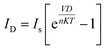
GeSn compounds have made many interesting contributions in photodetectors (PDs) over the last ten years, as they have a detection limit in the NIR and mid-IR region. Sn incorporation in Ge alters the cut off wavelength. In the present article, p–i–n structures based on GeSn junctions were fabricated to serve as PDs. Arsine (As) is incorporated to develop n-GeSn compounds via a metal induced crystallization (MIC) process followed by i-GeSn on p-Si wafers. The impact of As and Sn doping on the strain characteristics of GeSn has been studied with high resolution transmission electron microscopy (HRTEM), X-ray diffraction and Raman spectroscopy analyses. The direct transitions and tuning of their band energies have been investigated using diffuse reflectance UV-vis spectroscopy and photoluminescence (PL). The barrier height and spectral responsivity have been controlled with incorporation of As. Variation of As incorporation into GeSn Compounds shifted the Raman peak and hence affected the strain in the Ge network. UV-vis spectroscopy showed that the direct transition energies are lowered as the Ge–As bonding increases as illustrated in Raman spectroscopy investigations. PL and UV-vis spectroscopy of annealed heterostructures at 500 °C showed that there are many transition peaks from the UV to the NIR region as result of oxygen vacancies in the Ge network. The calculated diode parameters showed that As incorporation leads to an increase of the height barrier and thus dark current. Spectral response measurements show that the prepared heterojunctions have spectral responses in near UV and NIR regions that gives them opportunities in UV and NIR photodetection-applications.
Introduction
Direct transition semiconducting materials are involved in photodetection applications. Highly responsive photodetectors generate electron–hole pairs via direct photonic transition of electrons from the valence band to the conduction band by only photon excitation. However, in indirect semiconducting materials, a phononic transition is required using another photon, and then band-to-band photonic transition occurs.1,2 GeSn compounds exhibit a direct band gap transition because of the incorporation of Sn in Ge networks that modulates the Γ and L valley of the conduction band.3 The energy difference between the two values is then equal to zero and the transition is undergone directly.4,5 As a result of the modulated band gap in GeSn, their compounds have made a good contribution in mid-IR and NIR photodetection applications throughout the last decade.6 Many attempts investigated responsivity enhancement and adjusting the cut off wavelength of GeSn based PDs.7,8 J. Werner et al. compared Ge PDs and GeSn based PDs with 0.5% Sn content. The photodetector consisted of an i-GeSn layer sandwiched between a p-Ge bottom layer and n-Ge cap layer on a Ge/Si virtual substrate. They measured responsivity with a value of 0.1 A W−1 with a cut off edge wavelength of 1.55 μm compared to the Ge PD with 0.03 A W−1 responsivity and higher dark current and a shorter cut off wavelength with a value of 1.5 μm.9 M. Oehme et al. studied the effect of Sn content increasing in i-GeSn layer capped by n-Ge on p-Ge. They varied the Sn content from 1.9% to 4% and found the cut off wavelength increasing with increasing Sn content from 1600 nm up to 2000 nm and the dark current increases with the increasing of Sn content.10 M. Oehme et al. used multi quantum wells configurations instead of the GeSn layer. They altered the thickness of the GeSn well (dGeSn) from 6 nm up to 12 nm. They found that the cut off wavelength increases with the increase of the thickness of GeSn well since the smaller thickness of the well causes quantum confinement and widens the energy gap. The responsivity also increased as increasing the Sn metal.11 Kuo-Chih Lee et al. used a new configuration in which i-GeSn of a thickness of 163 nm is deposited on Ge virtual substrate and on both sides of i-GeSn layer, layers of p and n-Ge are deposited. They get a high responsivity of value 0.25 A W−1 at a cutoff wavelength of 1550 nm.12 Harshvardhan Kumar et al. fabricated homojunction of p–i–n GeSn layers with 0%, 3%, 6% and 9% of Sn content. They found that the cut off wavelength increased with the increase of Sn content starting from 2000 nm to 2500 nm and the responsivity increased up to 3.5 A W−1.13 Xiang Quan Liu et al. deposited a layer of GeSn on Ge virtual substrate. They altered the concentration of Sn via adjusting the growth temperature in a molecular beam epitaxy reactor. They reached 16.3% of Sn content at growth temperature equal 150 °C and Sn crucible temperature of value 760–835 °C. They get cut off wavelength up to 4 μm.14
In this work, metal induced crystallization of thermally evaporated amorphous Ge layers was employed to incorporate the Sn for tensile Ge network and As as n-type dopant during the low vacuum level annealing process. As a result of low vacuum level, oxygen is incorporated inside Ge networks. We get direct transition doped Ge. The effect of As incorporation on the tensile strain of Ge network has been investigated. Controlling the barrier height and so on the dark current via As doping are studied and how As incorporation reduces the energies of the direct transitions. Edge detection and responsivity of the prepared p–i–n junctions are also demonstrated.
Materials and methods
p–i–n junctions' fabrication
Four different configurations of semiconducting layers sandwiched between metal layers were deposited on single crystalline p-Si substrate using thermal evaporation technique (EDWARDS E306A). These layers were deposited under a vacuum of 6.5 × 10⁻⁵ mbar and then annealed at 500 °C inside the evacuated jar with low vacuum level equal to 4.6 × 10⁻² mbar for 24 h. The first configuration consists of 250 nm of silicon covered by 100 nm of Sn followed by 250 nm of Ge layer capped by 10 nm of As. As a result, metal induced crystallization (MIC) has occurred and Sn, As metals diffused in the semiconducting layers forming an intrinsic GeSn layer covered by As doped Ge. Because of the low vacuum level during the annealing process, oxygen vacancies occupy the defects in Ge networks and formed GeOx. The second configuration has the same silicon layer covered by Sn and the germanium layer capped with a Sn layer. After annealing, a 10 nm of As layer is deposited on the GeSn layer to form n-GeSn. The third configuration is the same as the first configuration except that a silicon layer is replaced by a Ge layer. The fourth configuration has the same structure as the second configuration but the silicon layer in the second configuration is also replaced by Ge layer. Four different structured p–i–n junctions are formed to serve as photodiodes as shown in Fig. 1.
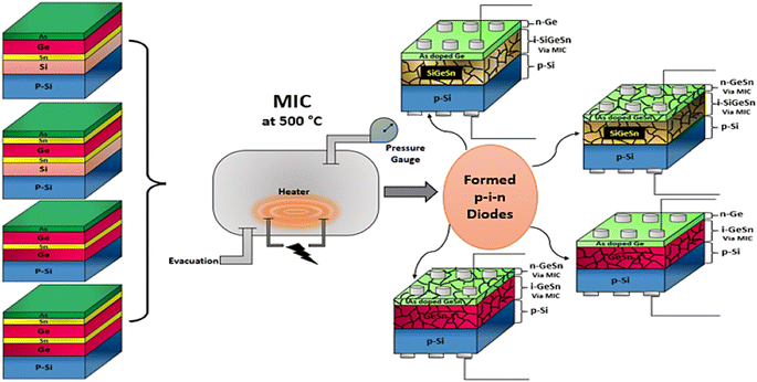 |
| | Fig. 1 Formation of GeSn based p–i–n diodes via metal induced crystallization (MIC). | |
Investigation of strain in Ge crystallites formed by MIC
High resolution transmission electron microscopy. High resolution transmission electron microscopy was involved to investigate the Sn and As doped Ge strain crystallites formation during MIC process. A JEOL JEM-2100 plus HRTEM operating at 200 kV was used to calculate the d-spacing in the grown planes of strained Ge crystallites. Energy dispersion X-ray analysis (EDX) setup is attached to investigate the elemental analysis of the measured sample, which was peeled from the top surface of the fabricated film and dispersed in ethanol with ultrasonication for 15 minutes.
X-Ray diffraction analysis. A Shimadzu LabX 6000 X-ray diffractometer was utilized to investigate the formation of GeSn crystallites as a result of Sn incorporation inside Ge network. d-Spacing, growth orientations, and microstrain were investigated using XRD measurements.
Raman spectroscopy. Raman spectroscopy is used to investigate the tensile strain Ge networks in the prepared p–i–n junctions in term of Raman shifting using Witec Raman confocal microscope with an excitation laser wavelength of 352 nm.
Direct transition investigation
Direct transition of the formed compounds and their band gap as a function of As content were studied using diffuse reflectance spectrophotometer (UV-vis-NIR JASCO V-770). He–Cd laser (Kimmon – 325 nm) was used as excitation source for photoluminescence. The spectra are collected using iHR320 spectrometer (HORIBA) equipped with a Synapse CCD camera ranging between 300 nm to 1500 nm for detection.
Hall effect, dark current and barrier height calculations
Negative charge carrier concentration as a function of As content was measured using Ecopia HMS 3000 Hall measurement system at room temperature ≈298 K. A Potentiostat METROHM Autolab 87070 was used to study the I–V characteristics of the formed p–i–n junctions biased by −5 and +5 V. Dark current and barrier height dependence on As were calculated.
Spectral responsivity and cut off wavelength measurements
Spectral responsivity of the prepared heterojunctions has been measured using PVE300 system with 75 W xenon lamp of spectral range between 300–1100 nm and 1100–2500 nm, respectively. The photodetectors used in the system are silicon PD with a detection range between 300–1100 nm and germanium PD with detection range between 800–1800 nm.
Results and discussion
HRTEM analysis
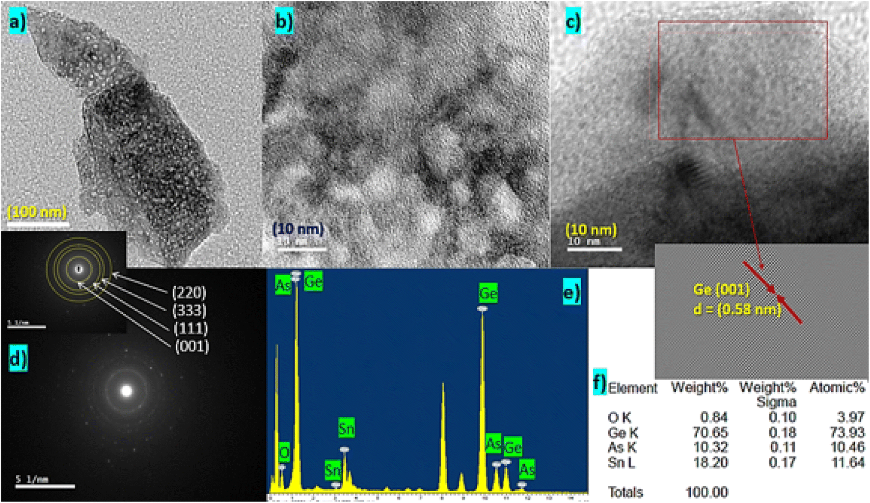
Low and high-resolution transmission electron microscopy were involved to investigate the Sn and As doped Ge crystallites during MIC process. Fig. 2a–c shows low and HRTEM micrographs of the annealed Ge/Sn/Ge/As multilayers on p-Si substrate. It is observed that there are crystallites of Ge formed after the layers interdiffusion during MIC process.15–17 Fig. 2b and c shows multiple orientations of the grown Ge crystallites with d-spacing value of 0.58 nm of strained Ge (001). Fig. 2e and f shows the EDX spectra of the prepared sample and the percentage of the elements forming the heterostructure in a selected area. The elemental analysis shows the existence of As and Sn metals that are incorporated in the Ge with an atomic percentage of 10.46% and 11.64%, respectively. Oxygen atoms with a percentage of 3.97% is detected during the annealing process and filled the vacancies in the Ge network. Selected area electron diffraction (SAED) indicates that there are four orientations of (001), (111), (333), and (220) of the strained Ge planes doped with Sn (JCPDS card no. 65-0333).18 The d-spacing values of these planes are estimated from the SAED. Table 1 summarizes the calculated d-spacing values of these interplanar spacing that are 0.5846, 0.3576, 0.302, and 0.2361 nm for the mentioned planes, respectively. These values of the strained planes are larger than the values of pure germanium (0.5513, 0.3276, 0.2935, and 0.2006 nm) for the same planes, respectively.18 This indicates that Sn atoms with large diameter incorporated inside the Ge network and increased the d-spacing values in Ge network.19
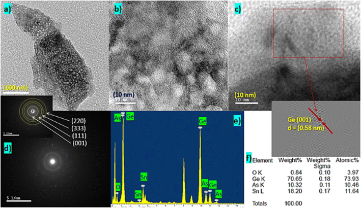 |
| | Fig. 2 (a–c) Low and HRTEM images of a prepared Ge/Sn/Ge/As configuration on p-Si substrate after MIC, (d) selected area electron diffraction, (e) EDX spectra, and (f) the atomic and weight percentage of the elements forming the sample. | |
Table 1 The calculated d-spacing of the strained Ge planes
| Ge planes |
1/2r (1/nm) |
d-Spacing (nm) |
| (001) |
3.421 |
0.5846 |
| (111) |
5.593 |
0.3576 |
| (333) |
6.623 |
0.302 |
| (220) |
8.467 |
0.2362 |
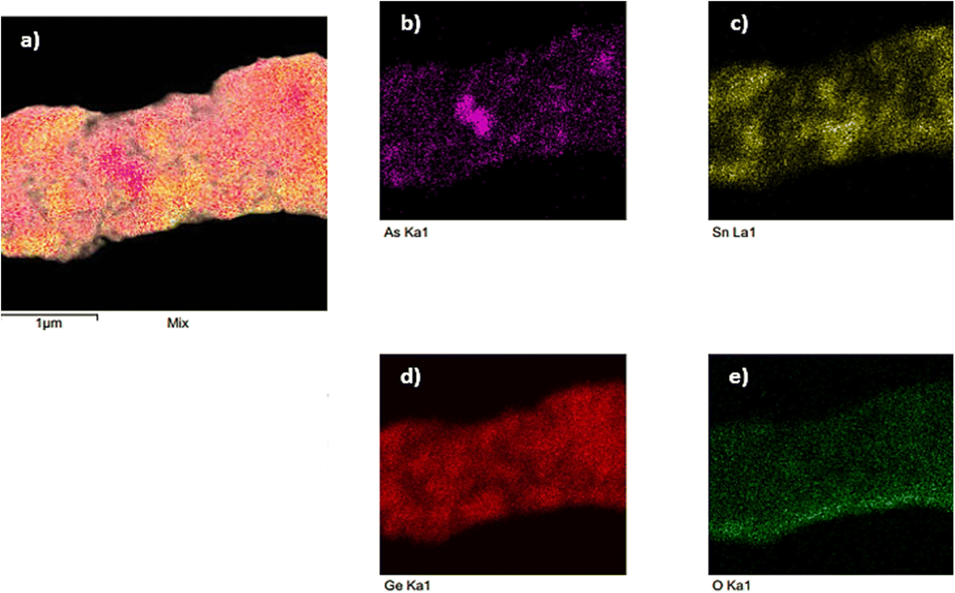
Elemental mapping analysis was carried out for Ge/Sn/Ge/As annealed on p-Si. The mapping analysis shows uniform space distribution of the Ge, Sn, As, and O atoms that compose the prepared sample. Fig. 3a shows the mixture of the composing elements. Fig. 3b–e shows uniform distribution of As, Sn, Ge, and O, respectively.
 |
| | Fig. 3 Elemental mapping analysis of prepared Ge/Sn/Ge/As configuration annealed on p-Si. | |
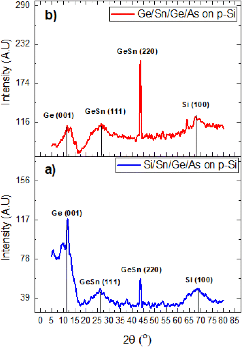
XRD analysis
XRD analysis was carried out for the Si/Sn/Ge/As and Ge/Sn/Ge/As configurations on p-Si annealed at 500 °C. Fig. 4 shows the XRD patterns of the two configurations. Ge (001), GeSn (111) broad peaks and GeSn (220) intense sharp peak were detected for both configurations.20–23 The appearance of these planes matches with the HRTEM data. The most intense peak is GeSn (220) peak that is detected at 2θ = 43.8° and 43.72° for Si/Sn/Ge/As and Ge/Sn/Ge/As configurations on p-Si annealed at 500 °C, respectively. Ge (001) peak intensity is reduced in the second configuration in which the GeSn (220) peak increases. The second configuration's GeSn crystals seems highly oriented in (220) direction. Si (100) broad peak appears because of (100) p-Si oriented substrate that is covered by the deposited configurations.24 The estimated d-spacing of the (220) oriented GeSn plane is 0.2221 and 0.2234 nm for the first and the second above mentioned configurations. The value of d-spacing form XRD analysis is very close to the d-spacing value of the GeSn (220) estimated from the SEAD measurements. The increase in the d-spacing for both configurations compared with the reference Ge is due to the large radii Sn atoms incorporation. This will cause compressive strain in Ge network.25 The evidence for the compressive strain is the left shift of the GeSn peak (220). The value of the compressive strain in GeSn (220) plane was calculated using Williamson Hall equation ε = β/4![[thin space (1/6-em)]](https://www.rsc.org/images/entities/char_2009.gif) tanθ.26 The values of the strain are 4.37 × 10⁻³ and 4.01 × 10⁻³ for the first and the second configuration, respectively. It is observed that the GeSn (220) in the second configuration (Ge/Sn/Ge/As) shifted to lower angle than in the first one (Si/Sn/Ge/Sn) as mentioned above. This is because of the higher thickness of the germanium layers in the second configuration. This causes relaxation in Ge network and incorporation more Sn atoms. due to Sn incorporation. This compressive strain relaxation makes the Ge network accept more Sn atoms that increase the structure compression.27
tanθ.26 The values of the strain are 4.37 × 10⁻³ and 4.01 × 10⁻³ for the first and the second configuration, respectively. It is observed that the GeSn (220) in the second configuration (Ge/Sn/Ge/As) shifted to lower angle than in the first one (Si/Sn/Ge/Sn) as mentioned above. This is because of the higher thickness of the germanium layers in the second configuration. This causes relaxation in Ge network and incorporation more Sn atoms. due to Sn incorporation. This compressive strain relaxation makes the Ge network accept more Sn atoms that increase the structure compression.27
 |
| | Fig. 4 XRD patterns of (a) Si/Sn/Ge/As and (b) Ge/Sn/Ge/As configurations on p-Si annealed at 500 °C. | |
Raman analyses
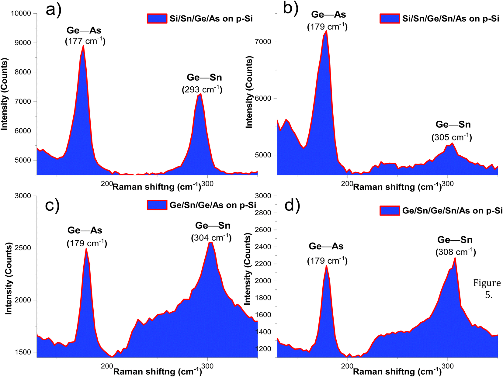
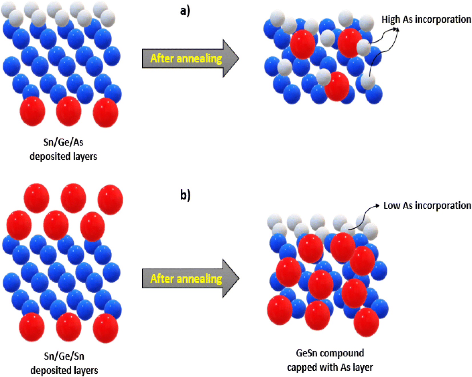
Fig. 5a–d shows the Raman spectra of the mentioned prepared configurations. A peak is detected for all configuration around 300 cm−1 which refers to GeSn mode.28 The intensity of this peak is higher in configurations that contain Si buffer layer up to 7000 counts than the others don't have Si of intensity value ≈2500 counts. This is due to the solubility of Sn in Si layer is lower than in Ge during MIC because of the higher phase mismatching between Si and Sn than between Ge and Sn,29 see Fig. 6. This reason caused higher incorporation of Sn in Ge in these configurations that contain Si buffer. Fig. 5a–d also shows a peak at 179 cm−1 corresponding to GeAs mode.30 The intensity of the GeSn peak is higher in configurations in which As is incorporated during annealing process. To explain the Raman shift in all configurations, the involved strains should be explained. In previous work, we studied the strain effect of Sn incorporation inside Ge network involved in identical Ge and Sn layers with the present work using XRD technique.15 The interdiffusion between Sn and Ge interfaces was demonstrated using FESEM and HRTEM. It was shown that there is a compressive strain of Ge network in its interface with Si buffer due to the mismatching between Si and Ge lattice constants and atomic radii.19 A compressive strain occurred due to the Sn incorporation inside Ge network. Sn has larger atomic radii that causes compression of the bond lengths of Ge network.31 This results in shifting the GeSn peak towards lower wavenumbers. Interstitial doping of As has an impact in Raman shifting.32 The peak position of GeSn of the first configuration is at 293 cm−1 in which As is incorporated during annealing while the peak position of the corresponding second configuration in which As isn't incorporated via annealing was detected at 305 cm−1. The GeSn peak of the other configurations is shifted from 308 cm−1 to 304 cm−1 which enhances the direct transition in Ge network.33
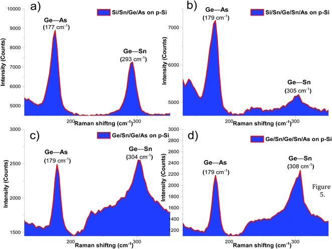 |
| | Fig. 5 Raman shifting of the prepared heterostructures (a) Si/Sn/Ge/As on p-Si, (b) Si/Sn/Ge/Sn/As on p-Si, (c) Ge/Sn/Ge/As on p-Si and (d) Ge/Sn/Ge/Sn/As on p-Si. | |
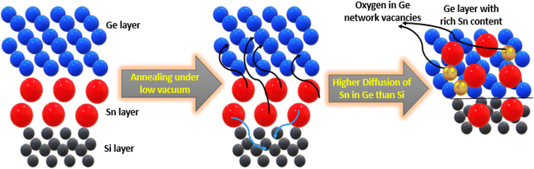 |
| | Fig. 6 Sn solubility in Ge rather than Si. | |
Investigation of direct band gap using diffuse reflectance spectroscopy
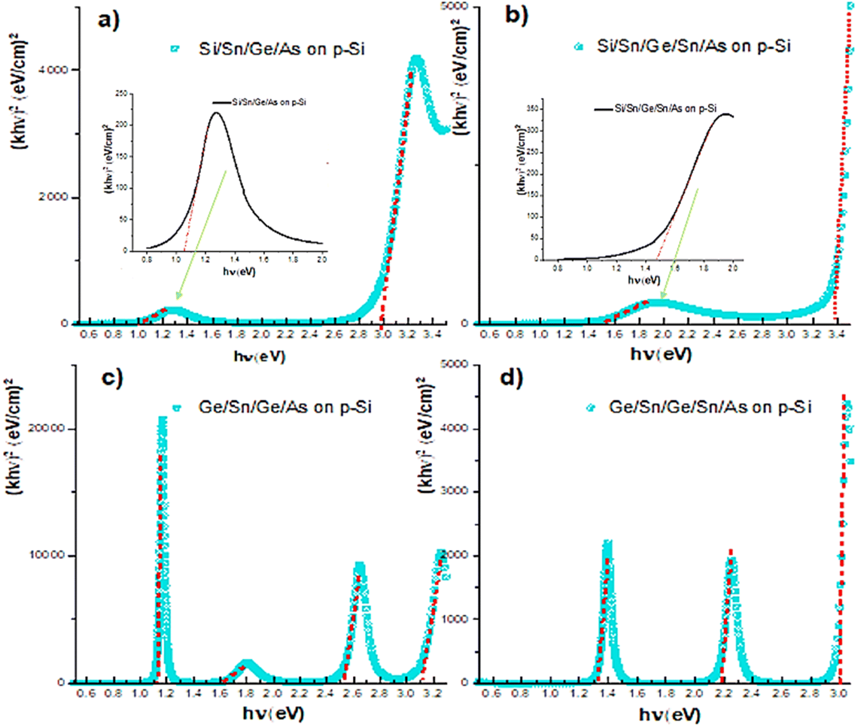
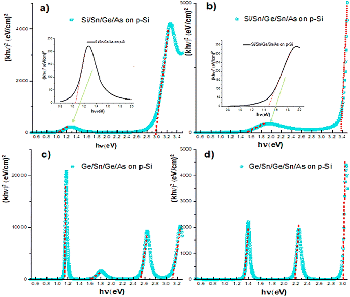
Diffuse reflectance UV-vis spectroscopy was involved to investigate the direct transition in Ge crystallites in which Sn and As were incorporated during MIC process as well as introducing oxygen vacancies inside Ge networks. Kubelka–Munk model is used to estimate the values of the direct band gap of the prepared p–i–n heterostructures.34 Fig. 7a–d shows plots of (khν)2 versus hν of the prepared heterostructures. Weak direct transitions values are extrapolated at 1.05 eV to 1.47 eV for Si/Sn/Ge/As and Si/Sn/Ge/Sn/As respectively, see the insets of Fig. 7a and b. These weak direct transitions may correspond to the formed GeSn crystallites with oxygen atoms occupied the vacancies in Ge network. This oxidation of Ge incorporated with Sn makes the band gap wider.35 The shifting of the transition towards low energy of 1.05 eV in Si/Sn/Ge/As than the other configuration is due to As incorporation during high temperature annealing forming shallow levels near conduction band that reducing the gap, See Fig. 8 and 9a in the manuscript.36 These values of the transitions agree with the NIR (1255 nm) peak in PL measurements and the photoresponsivity edge in NIR at 1181 nm (1.0498 eV) as we will discuss in the following section.
 |
| | Fig. 7 (khν)2 versus hν plot of the prepared heterostructures. | |
 |
| | Fig. 8 Deep As incorporation inside Ge network during annealing process. | |
 |
| | Fig. 9 (a) Indirect to direct transition band gap due to Sn and As incorporation in strained Ge network. (b) Photoluminescence spectra of the prepared heterostructures. | |
Fig. 7c and d shows the direct transitions in Ge/Sn/Ge/As and Ge/Sn/Ge/Sn/As respectively. It is observed that a strong direct transition at 1.1 eV and 1.33 eV for the two mentioned configurations respectively.
Another direct transition at 2.9 eV and 3.38 eV is due to oxidation level during the annealing process under low vacuum forming GeO2 that has these wide band gaps as shown in Fig. 6.37,38 This direct transition is due to strained GeSn formed crystallites with oxygen vacancies during low vacuum annealing process.39 The transitions in the configurations that contain only Ge layers shift towards high energy than the configurations contain Si. This is because Sn has higher solubility in Ge than in Si thus the atoms of Sn layers will mostly diffuse in Ge rather than Si causing GeSn crystallites nucleation and growth in the above Ge and Sn layers on Si layer.16 On the other hand, the atoms of Sn layers in the configurations contain only Ge layers diffuse in two Ge layers resulting in low Sn content in each Ge layer, see Fig. 6. As a result of low Sn content layers, the energy gap gets widened. Two other direct transitions are observed; one is at 2.5 eV, 2.17 eV for Ge/Sn/Ge/As and Ge/Sn/Ge/Sn/As respectively, and the other is at 3.1 eV and 3 eV for Ge/Sn/Ge/As and Ge/Sn/Ge/Sn/As respectively. These transitions are due to the formed GeOx with different levels of oxygen vacancies at the two different Ge layers during the annealing process.38,39
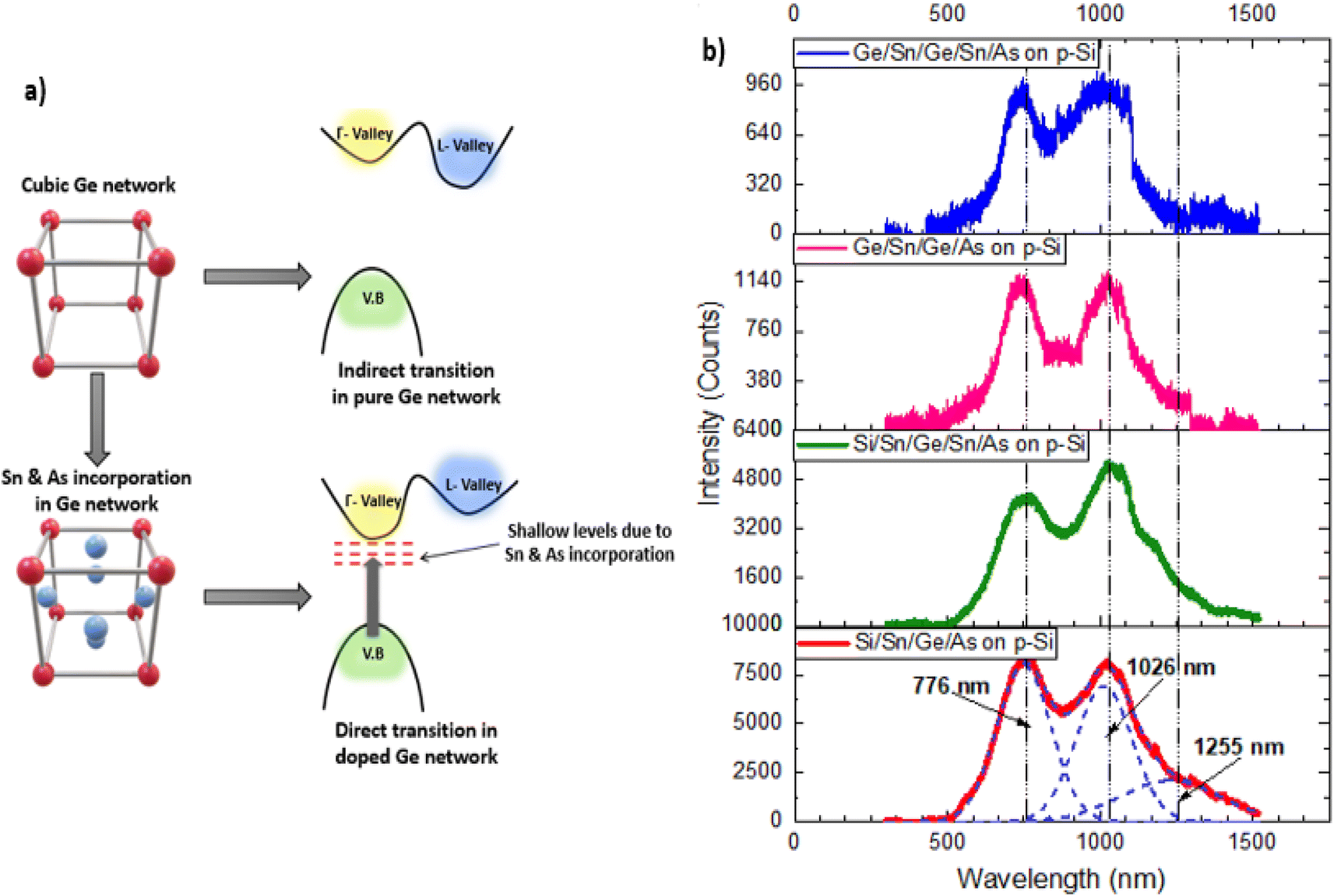
Photoluminescence measurements
The Sn and As were incorporated in Ge networks within MIC process.40 The role of Sn in the Ge networks is to form GeSn compound that has a direct transition band gap as Sn incorporation modulated the energy difference between L-valley and Γ-valley.41 The energy of Γ-valley increases that is aligned to the valence band forming direct transition band gap in the strained Ge networks doped with Sn and the energy gap gets lower. The incorporation of As on the surface of the prepared structure formed n-GeSn layer with shallow levels of As charge carriers inside the energy gap causes the band gap get narrower, See Fig. (9a). Fig. 9b shows the photoluminescence spectra of the prepared p–i–n structures. Three main overlapped peaks over wide range of spectra between 550 nm to 1500 nm (visible-NIR) is observed. The first peak is detected at 776 nm which is due to the p-Si base substrate after thermal oxidation and few contributions of poly-Si crystallites formed via MIC.42 The second peak is at 1026 nm that is due to oxidized Ge network doped with Sn.43 A 1255 nm low intensity peak is detected due to the oxidized GeSn doped with As that introduces shallow levels within the energy gap that makes it get narrower.36,43 This gives these p–i–n structures the chance to serve as optically pumped white light and NIR source.15 It is observed that the heterostructures containing Si layer have higher intensity of PL peak due the enhancing of Si in MIC process of Ge as we discussed before.
Dark current and barrier height calculations using IV characteristics investigations
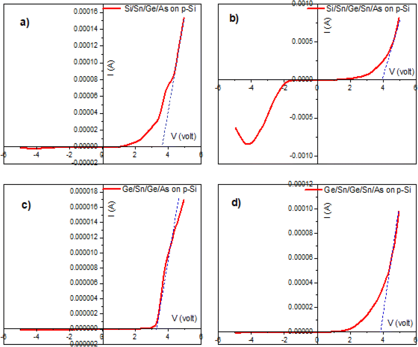
After the annealing process under low vacuum level, MIC process occurred and As is diffused in the formed strained GeSn compound. The resultant heterostructures consisted of n-GeSn doped with As above i-GeSn or i-SiGeSn formed on p-Si base substrate to get p–i–n junctions. Ag back and front grid electrodes were deposited on the p-Si and n-GeSn layer for Hall effect and IV characteristics measurements. Hall effect measurement was carried out by Ecopia HMS 3000 Hall measurement system to determine the negative charge carrier concentration due to As addition to germanium. Hall effect measurements revealed that the negative charge carrier concentration was −2.465 × 10¹⁴ e cm−3 with high electron mobility. The electron mobility was 1.219 × 103 cm2 V−1 s−1. This high electron mobility is due to the high annealing temperature up to 500 °C. This high annealing temperature releases the strain in germanium and causes large accumulation of germanium crystallites resulting in reducing grain boundaries.44,45 IV characteristics of the resultant junctions were carried out as shown in Fig. 10 using a METROHM Autolab 87070 potentiostat system.
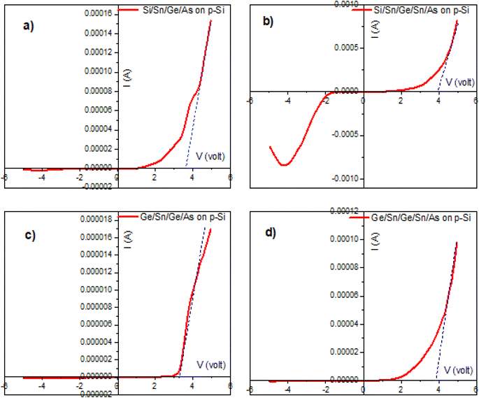 |
| | Fig. 10 I–V characteristic plot of the prepared heterostructures in ±5 V forward and reverse biasing (a) Si/Sn/Ge/As on p-Si, (b) Si/Sn/Ge/Sn/As on p-Si, (c) Ge/Sn/Ge/As on p-Si, and (d) Ge/Sn/Ge/Sn/As on p-Si. | |
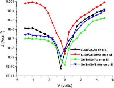
Fig. 10a–d shows the IV measurements for the fabricated heterostructures (n-GeSn/i-SiGeSn/p-Si) and (n-GeSn/i-GeSn/p-Si) biased by ±5 V. Turn-on voltage of the four junctions is estimated from Fig. 10 and so the dark current at −5 V. Table 2 summarizes the calculated diode parameters for the prepared p–i–n configurations. Fig. 11 shows a plot of the current in logarithmic scale versus voltage. It is found that the dark current for Si/Sn/Ge/As, Ge/Sn/Ge/As and Ge/Sn/Ge/Sn/As is very low in range of 10−7–10−8 A cm−2 compared to other works46–49 except Si/Sn/Ge/Sn/As on p-Si that has higher dark current of value 4.87 × 10⁻⁴ A cm−2 at −3 V. According to Raman shifting measurements, this configuration has lower bonding between Ge and Sn that causes free Sn clusters to serve in the dark current.
Table 2 The calculated diode parameters of the prepared p–i–n junctions
| Sample |
Turn-on voltage (V) |
Quality factor “n” |
Barrier height ϕB (eV) |
Dark current at −3 V (A cm−2) |
| Region 1 |
Region 2 |
| Si/Sn/Ge/As on p-Si |
3.65 |
1.73 |
2.94 |
0.77 |
5.29 × 10⁻⁷ |
| Si/Sn/Ge/Sn/As on p-Si |
3.95 |
2.34 |
2.28 |
0.61 |
4.87 × 10⁻⁴ |
| Ge/Sn/Ge/As on p-Si |
3.35 |
1.33 |
5.62 |
0.84 |
8.26 × 10⁻⁸ |
| Ge/Sn/Ge/Sn/As on p-Si |
3.87 |
1.07 |
2.51 |
0.81 |
1.98 × 10⁻⁷ |
 |
| | Fig. 11 The current density in logarithmic scale versus voltage of the prepared p–i–n junctions. | |
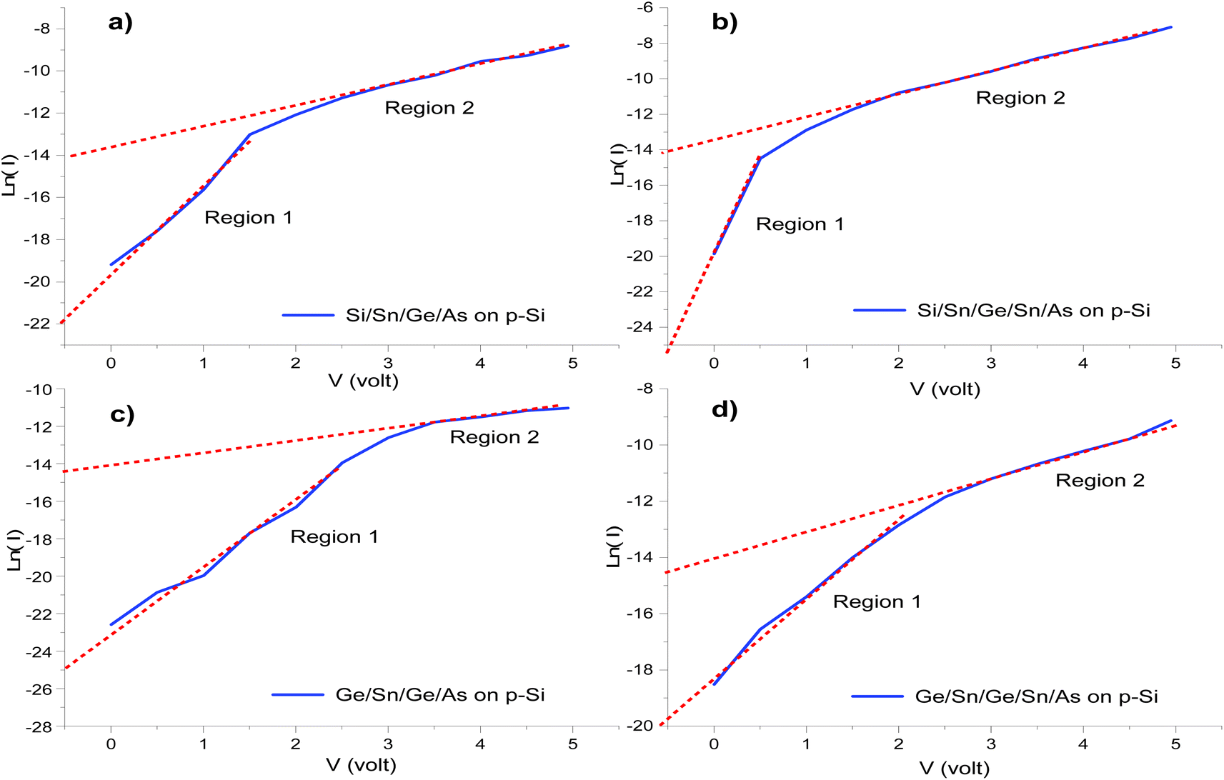
The turn-on voltage has values ranged between 3.35 V to 3.95 V. It is found that the turn-on voltage decreases in the configurations (Si/Sn/Ge/As and Ge/Sn/Ge/As on p-Si) in which As is deeply incorporated inside GeSn during the annealing process that increases the n-type charge carrier and thus reduce depletion region.50
The diodes quality factors have been calculated using Schottky diode equation51 at low voltage (region 1) and high voltage (region 2, see Fig. 12a–d).
| |
 | (1) |
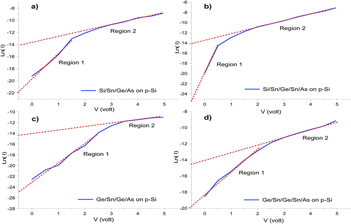 |
| | Fig. 12 Plot of ln(I) versus V for the prepared junctions. (a) Si/Sn/Ge/As, (b) Si/Sn/Ge/Sn/As, (c) Ge/Sn/Ge/As, and (d) Ge/Sn/Ge/Sn/As on p-Si. | |
The values of the quality factor are estimated from the slope of ln(I) versus V plot as seen in Fig. 12. They are listed in Table 2. It is observed that the values are near ideality at low voltage region. The configurations that contain only Ge semiconductor layers (Ge/Sn/Ge/As and Ge/Sn/Ge/Sn/As on p-Si) have ideality factors of values 1.33 and 1.07 that are near ideal diode factor = 1 rather than the other configurations contain Si layers. The non-ideal factors of the prepared junctions that have values above 2 up to 5.61 at higher voltage region due to the tunneling effect of the conduction electrons of Sn and As metals at high voltage that increases the saturation dark current increasing the ideality factor above the ideality.52
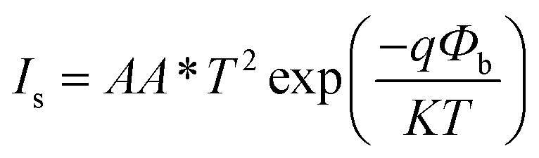
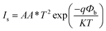
To get a high response photodetector, the photocurrent must be higher above the reverse dark current. Higher barrier height prevents the reverse diffusion current from the n-type to the p-type.53 Thus, the depletion region barrier height is responsible for the high-quality photodetectors. The barrier heights of the prepared junctions are estimated using Richardson equation:51
| |
 | (2) |
where
A is the area of the diode,
A* is Richardson constant,
q is the charge of electron,
K is Boltzmann constant,
T is temperature in Kelvin and
ϕb is the barrier height. The barrier heights of the prepared p–i–n junctions are calculated and listed in
Table 2. It is seen that the barrier heights of the prepared junctions range between 0.61 to 0.84 eV and are higher than the barrier height of germanium-based diodes, which have values in the range of 0.2–0.3 eV.
54,55 This gives the prepared samples a good chance to contribute to germanium based photodetection applications.
The responsivity measurements of the prepared GeSn based PDs
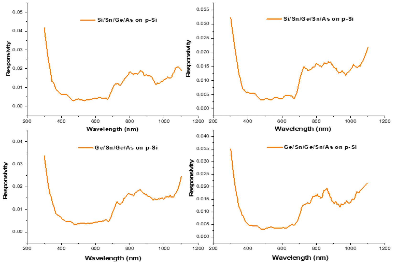
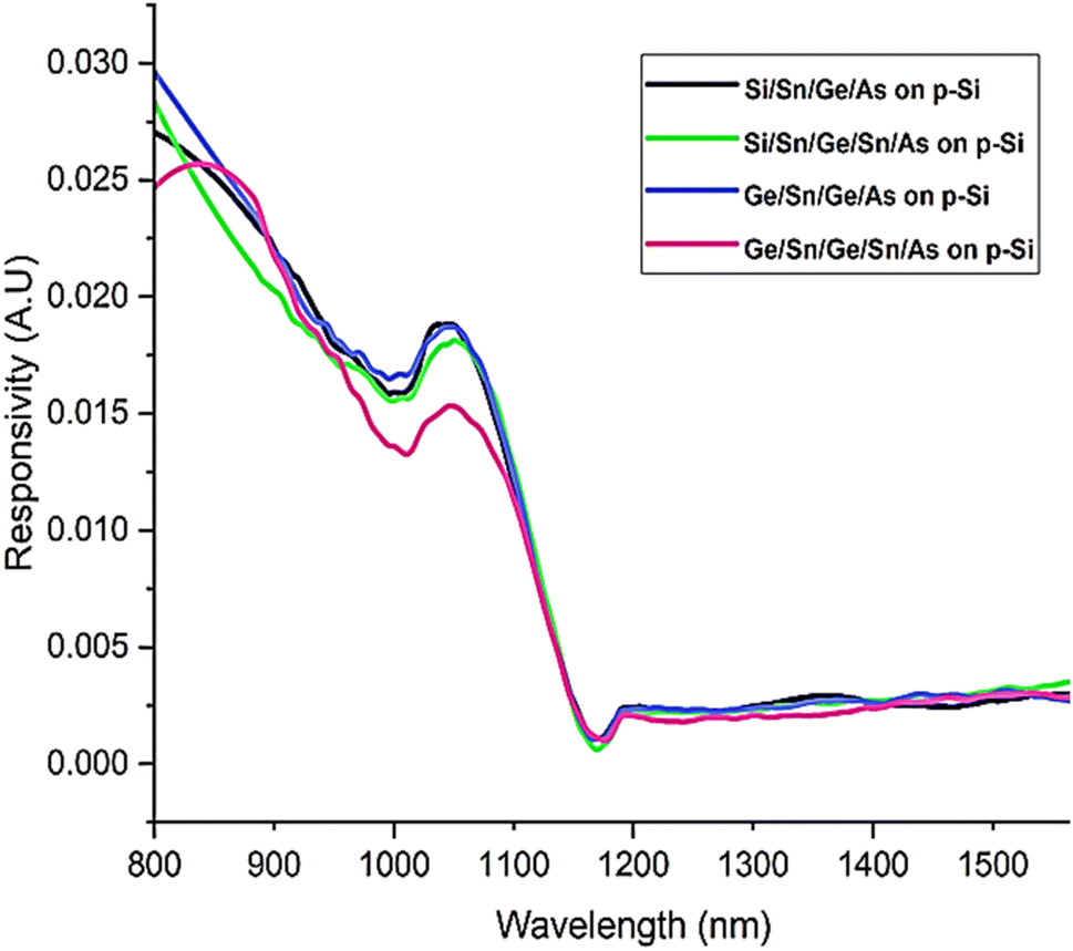
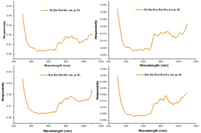
Responsivity measurements are carried out to investigate the detection region of the prepared p–i–n based GeSn heterostructures. The measurements reveal that the prepared heterostructures have a response near UV portion radiation as seen in Fig. 13. This can be explained as germanium networks doped with Sn and As of the prepared samples contain oxygen vacancies forming GeOx that has wide band gap that pushes UV spectrum to generate photocurrent56 as discussed in photoluminescence, UV-vis spectroscopy and Raman spectroscopy. Fig. 13 shows that the response decreases from near UV region to the visible. This gives the prepared p–i–n GeSn heterojunction the opportunity to be utilized as UV photodetectors. Fig. 14 shows that the samples have responsivity in NIR region from 800 nm to 1200 nm of values close to that in UV region. This response in NIR region is corresponding to the GeSn doped with arsenic with cut off wavelength at 1181 nm.
 |
| | Fig. 13 Responsivity of the prepared heterojunctions in (300 nm–1200 nm) spectral range. | |
 |
| | Fig. 14 Responsivity of the prepared heterojunctions in (800 nm–1600 nm) spectral range and cut off edge. | |
In this work, we aim to get spectral responsivity in different regions of spectra. Low vacuum conditions were involved during preparing these heterostructures. As a result of different levels of oxidation, the band gap values varied across the prepared heterostructures. Spectral responsivity measurements reveal that the prepared heterostructures at low vacuum condition have spectral response in both UV and NIR regions with cutoff wavelength at 1181 nm. It is known that Ge and GeSn based photodetectors have spectral responsivity in mid IR region with cut off wavelength in the range ≈(1600–3600 nm).57 Here, the oxygen filled the Ge crystallite vacancies widens the band gap across the prepared heterostructures as shown in UV-vis spectroscopy and photoluminescence measurements. This shifts the cut off wavelength of responsivity from mid IR (1600–3600 nm) region to NIR region at (1181 nm). This also gives these prepared heterostructures the chance to be used as UV and IR photodetectors.58
Conclusions
We fabricated two region (UV and NIR) p–i–n based GeSn photodetectors with the aid of the simple and low-cost metal induced crystallization of germanium technique. This technique served in oxygen incorporation that widened band gap up to 3.38 eV that enabled the prepared PDs to detect spectra below 300 nm. MIC also served in Sn and As incorporation and formation of strained Ge crystallites with d-spacing ≈0.22 nm for the highly oriented Ge (220) plane. This caused modulation of strained Ge crystallites band gap make it get narrower down to 1.05 eV. This gives the prepared PDs the ability to detect in NIR region with cut off wavelength near 1200 nm. Diode IV characteristics revealed that the dark current for Si/Sn/Ge/As, Ge/Sn/Ge/As and Ge/Sn/Ge/Sn/As is very low in range of 10−7 to 10−8 A cm−2, their ideality factors are near 1 and the barrier heights of the junctions are between 0.61 to 0.84 eV that higher than the barrier height of germanium-based reference diodes that make them promise in photodetection applications.
Data availability
The data that support the plots and results within this paper are available from the corresponding authors upon reasonable request.
Conflicts of interest
The authors declare no competing interests or non-financial interests.
Acknowledgements
We thank Dr Mostafa Sanad as he gives help in Hall effect measurements that were carried out at Central Metallurgical Research & Development Institute (CMRDI).
References
- X. Wang, Z. Cheng, K. Xu, H. K. Tsang and J. B. Xu, High-responsivity graphene/silicon-heterostructure waveguide photodetectors, Nat. Photonics, 2013, 7(11), 888–891 CrossRef CAS.
- R. A. Yotter and D. M. Wilson, A review of photodetectors for sensing light-emitting reporters in biological systems, IEEE Sens. J., 2003, 3(3), 288–303 CrossRef CAS.
- R. Soref, J. Kouvetakis and J. Menendez, Advances in SiGeSn/Ge technology, MRS Online Proc. Libr., 2006, 958, 0958-L01 Search PubMed.
- H. S. Mączko, R. Kudrawiec and M. Gladysiewicz, Material gain engineering in GeSn/Ge quantum wells integrated with an Si platform, Sci. Rep., 2016, 6(1), 1–11 CrossRef PubMed.
- S. Barth, M. S. Seifner and S. Maldonado, Metastable group IV allotropes and solid solutions: nanoparticles and nanowires, Chem. Mater., 2020, 32(7), 2703–2741 CrossRef CAS.
- J. Doherty, S. Biswas, E. Galluccio, C. A. Broderick, A. Garcia-Gil, R. Duffy and J. D. Holmes, Progress on germanium–tin nanoscale alloys, Chem. Mater., 2020, 32(11), 4383–4408 CrossRef CAS.
- Y. H. Huang, G. E. Chang, H. Li and H. H. Cheng, Sn-based waveguide pin photodetector with strained GeSn/Ge multiple-quantum-well active layer, Opt. Lett., 2017, 42(9), 1652–1655 CrossRef CAS PubMed.
- G. E. Chang, S. Q. Yu, J. Liu, H. H. Cheng, R. A. Soref and G. Sun, Achievable performance of uncooled homojunction GeSn mid-infrared photodetectors, IEEE J. Sel. Top. Quantum Electron., 2021, 28(2), 1–11 Search PubMed.
- J. Werner, M. Oehme, M. Schmid, M. Kaschel, A. Schirmer, E. Kasper and J. Schulze, Germanium–tin pin photodetectors integrated on silicon grown by molecular beam epitaxy, Appl. Phys. Lett., 2011, 98(6), 061108 CrossRef.
- M. Oehme, M. Schmid, M. Kaschel, M. Gollhofer, D. Widmann, E. Kasper and J. Schulze, GeSn pin detectors integrated on Si with up to 4% Sn, Appl. Phys. Lett., 2012, 101(14), 141110 CrossRef.
- M. Oehme, D. Widmann, K. Kostecki, P. Zaumseil, B. Schwartz, M. Gollhofer and J. Schulze, GeSn/Ge multiquantum well photodetectors on Si substrates, Opt. Lett., 2014, 39(16), 4711–4714 CrossRef CAS PubMed.
- K. C. Lee, M. X. Lin, H. Li, H. H. Cheng, G. Sun, R. Soref and A. Medvids, Planar GeSn photodiode for high-detectivity photodetection at 1550 nm, Appl. Phys. Lett., 2020, 117(1), 012102 CrossRef CAS.
- H. Kumar and R. Basu, Design of Mid-Infrared Ge1−x Snx Homojunction pin Photodiodes on Si Substrate, IEEE Sens. J., 2022, 22(8), 7743–7751 CAS.
- X. Liu, J. Zheng, C. Niu, T. Liu, Q. Huang, M. Li and B. Cheng, Sn content gradient GeSn with strain controlled for high performance GeSn mid-infrared photodetectors, Photonics Res., 2022, 10(7), 1567–1574 CrossRef.
- M. A. Nawwar, M. S. Abo Ghazala, L. M. Sharaf El-Deen, A. El-Shaer, B. Anis and A. E. H. Bashir Kashyout, Toward White Light Random Lasing Emission Based on Strained Nano Polygermanium Doped with Tin via Metal-Induced Crystallization (MIC), Cryst. Growth Des., 2023, 23(2), 751–768 CrossRef CAS.
- S. Biswas, J. Doherty, D. Saladukha, Q. Ramasse, D. Majumdar, M. Upmanyu and J. D. Holmes, Non-equilibrium induction of tin in germanium: towards direct bandgap Ge1−xSnx nanowires, Nat. Commun., 2016, 7(1), 11405 CrossRef CAS PubMed.
- D.
H. Kang and J. H. Park, Indium (In)-and tin (Sn)-based metal induced crystallization (MIC) on amorphous germanium (α-Ge), Mater. Res. Bull., 2014, 60, 814–818 CrossRef CAS.
- X. Gao, W. Luo, C. Zhong, D. Wexler, S. L. Chou, H. K. Liu and J. Z. Wang, Novel germanium/polypyrrole composite for high power lithium-ion batteries, Sci. Rep., 2014, 4(1), 6095 CrossRef CAS PubMed.
- S. Liu, A. C. Covian, J. A. Gardener, A. Akey, B. D. Levin, X. Wang and J. Liu, Growth of α-Sn on silicon by a reversed β-Sn to α-Sn phase transformation for quantum material integration, Commun. Mater., 2022, 3(1), 1–11 CrossRef.
- K. Takemura, U. Schwarz, K. Syassen, M. Hanfland, N. E. Christensen, D. L. Novikov and I. Loa, High-pressure Cmca and hcp phases of germanium, Phys. Rev. B: Condens. Matter Mater. Phys., 2000, 62(16), R10603 CrossRef CAS.
- L. Jin, D. Zhang, H. Zhang, J. Fang, Y. Liao, T. Zhou and V. G. Harris, Large area germanium tin nanometer optical film coatings on highly flexible aluminum substrates, Sci. Rep., 2016, 6(1), 1–6 CrossRef PubMed.
- M. Kim, W. Fan, J. H. Seo, N. Cho, S. C. Liu, D. Geng and Z. Ma, Polycrystalline GeSn thin films on Si formed by alloy evaporation, Appl. Phys. Express, 2015, 8(6), 061301 CrossRef.
- L. Zhang, H. Y. Hong, Y. S. Wang, C. Li, G. Y. Lin, S. Y. Chen and J. Y. Wang, Formation of high-Sn content polycrystalline GeSn films by pulsed laser annealing on co-sputtered amorphous GeSn on Ge substrate, Chin. Phys. B, 2017, 26(11), 116802 CrossRef.
- T. T. K. Chi, N. T. Le, B. T. T. Hien, D. Q. Trung and N. Q. Liem, Preparation of SERS substrates for the detection of organic molecules at low concentration, Commun. Phys., 2016, 26, 261–268 CrossRef.
- H. Li, J. Brouillet, A. Salas, X. Wang and J. Liu, Low temperature growth of high crystallinity GeSn on amorphous layers for advanced optoelectronics, Opt. Mater. Express, 2013, 3(9), 1385–1396 CrossRef.
- A. A. Akl and A. S. Hassanien, Microstructure and crystal imperfections of nanosized CdSxSe1−x thermally evaporated thin films, Superlattices Microstruct., 2015, 85, 67–81 CrossRef CAS.
- R. Chen, S. Gupta, Y. C. Huang, Y. Huo, C. W. Rudy, E. Sanchez and J. S. Harris, Demonstration of a Ge/GeSn/Ge quantum-well microdisk resonator on silicon: enabling high-quality Ge (Sn) materials for micro-and nanophotonics, Nano Lett., 2014, 14(1), 37–43 CrossRef CAS PubMed.
- D. Han, H. Ye, Y. Song, Z. Zhu, Y. Yang, Z. Yu and Z. Di, Analysis of Raman scattering from inclined GeSn/Ge dual-nanowire heterostructure on Ge (1 1 1) substrate, Appl. Surf. Sci., 2019, 463, 581–586 CrossRef CAS.
- S. Wirths, D. Buca and S. Mantl, Si–Ge–Sn alloys: from growth to applications, Prog. Cryst. Growth Charact. Mater., 2016, 62(1), 1–39 CrossRef CAS.
- A. Di Bartolomeo, A. Grillo, F. Giubileo, L. Camilli, J. Sun, D. Capista and M. Passacantando, Field emission from two-dimensional GeAs, J. Phys. D: Appl. Phys., 2020, 54(10), 105302 CrossRef.
- W. Dou, M. Benamara, A. Mosleh, J. Margetis, P. Grant, Y. Zhou and S. Q. Yu, Investigation of GeSn strain relaxation and spontaneous composition gradient for low-defect and high-Sn alloy growth, Sci. Rep., 2018, 8(1), 1–11 CAS.
- K. H. Lee, S. Bao, B. Wang, C. Wang, S. F. Yoon, J. Michel and C. S. Tan, Reduction of threading dislocation density in Ge/Si using a heavily As-doped Ge seed layer, AIP Adv., 2016, 6(2), 025028 CrossRef.
- S. Al-Kabi, S. A. Ghetmiri, J. Margetis, W. Du, A. Mosleh, M. Alher and S. Q. Yu, Optical characterization of Si-based Ge1−x Snx alloys with Sn compositions up to 12%, J. Electron. Mater., 2016, 45, 2133–2141 CrossRef CAS.
- M. L. Myrick, M. N. Simcock, M. Baranowski, H. Brooke, S. L. Morgan and J. N. McCutcheon, The Kubelka–Munk diffuse reflectance formula revisited, Appl. Spectrosc. Rev., 2011, 46(2), 140–165 CrossRef.
- M. Köhler, M. Pomaska, F. Lentz, F. Finger, U. Rau and K. Ding, Wet-chemical preparation of silicon tunnel oxides for transparent passivated contacts in crystalline silicon solar cells, ACS Appl. Mater. Interfaces, 2018, 10(17), 14259–14263 CrossRef PubMed.
- G. Kartopu, O. Oklobia, D. Turkay, D. R. Diercks, B. P. Gorman, V. Barrioz and S. J. Irvine, Study of thin film poly-crystalline CdTe solar cells presenting high acceptor concentrations achieved by in situ arsenic doping, Sol. Energy Mater. Sol. Cells, 2019, 194, 259–267 CrossRef CAS.
- S. Wang, H. Liu, T. Nishimura, K. Nagashio, K. Kita and A. Toriumi, Investigations on GeO Disproportionation Using X-ray Photoelectron Spectroscopy, ECS Trans., 2013, 50(9), 557 CrossRef.
- M. Zacharias and P. M. Fauchet, Blue luminescence in films containing Ge and GeO2 nanocrystals: the role of defects, Appl. Phys. Lett., 1997, 71(3), 380–382 CrossRef CAS.
- M. Zacharias and P. M. Fauchet, Blue luminescence in films containing Ge and GeO2 nanocrystals: the role of defects, Appl. Phys. Lett., 1997, 71(3), 380–382 CrossRef CAS.
- G. Maity, S. Dubey, T. Meher, S. Dhar, D. Kanjilal, T. Som and S. P. Patel, Perspectives on metal induced crystallization of a-Si and a-Ge thin films, RSC Adv., 2022, 12(52), 33899–33921 RSC.
- D. Stange, S. Wirths, N. von den Driesch, G. Mussler, T. Stoica, Z. Ikonic and D. Buca, Optical transitions in direct-bandgap Ge1−x Snx alloys, ACS Photonics, 2015, 2(11), 1539–1545 CrossRef CAS.
- S. Dellis, N. Pliatsikas, N. Kalfagiannis, O. Lidor-Shalev, A. Papaderakis, G. Vourlias and P. Patsalas, Broadband luminescence in defect-engineered electrochemically produced porous Si/ZnO nanostructures, Sci. Rep., 2018, 8(1), 1–8 CrossRef CAS PubMed.
- S. G. Cherkova, V. A. Volodin, F. Zhang, M. Stoffel, H. Rinnert and M. Vergnat, Optical properties of GeO [SiO] and GeO [SiO2] solid alloy layers grown at low temperature, Opt. Mater., 2021, 122, 111736 CrossRef CAS.
- L. Zhang, Y. Wang, N. Chen, G. Lin, C. Li, W. Huang and J. Wang, Raman scattering study of amorphous GeSn films and their crystallization on Si substrates, J. Non-Cryst. Solids, 2016, 448, 74–78 CrossRef CAS.
- Y. Shao, Y. Fang, T. Li, Q. Wang, Q. Dong, Y. Deng and J. Huang, Grain boundary dominated ion migration in polycrystalline organic–inorganic halide perovskite films, Energy Environ. Sci., 2016, 9(5), 1752–1759 RSC.
- H. Kumar and R. Basu, Design of Mid-Infrared Ge1−x Snx Homojunction pin Photodiodes on Si Substrate, IEEE Sens. J., 2022, 22(8), 7743–7751 CAS.
- M. R. Atalla, S. Assali, S. Koelling, A. Attiaoui and O. Moutanabbir, Dark current in monolithic extended-SWIR GeSn PIN photodetectors, Appl. Phys. Lett., 2023, 122(3), 031103 CrossRef CAS.
- H. Zhou, S. Xu, S. Wu, Y. C. Huang, P. Zhao, J. Tong and C. S. Tan, Photo detection and modulation from 1550 to 2000 nm realized by a GeSn/Ge multiple-quantum-well photodiode on a 300-μm Si substrate, Opt. Express, 2020, 28(23), 34772–34786 CrossRef CAS PubMed.
- M. Li, J. Zheng, X. Liu, Y. Zhu, C. Niu, Y. Pang and B. Cheng, Sn composition graded GeSn photodetectors on Si substrate with cutoff wavelength of 3.3 μm for mid-infrared Si photonics, Appl. Phys. Lett., 2022, 120(12), 121103 CrossRef CAS.
- A. Sutka, G. Mezinskis, A. Lusis and D. Jakovlevs, Influence of iron non-stoichiometry on spinel zinc ferrite gas sensing properties, Sens. Actuators, B, 2012, 171, 204–209 CrossRef.
- M. S. Abo Ghazala, H. A. Othman, L. M. Sharaf El-Deen, M. A. Nawwar and A. E. H. B. Kashyout, Fabrication of Nanocrystalline Silicon Thin Films Utilized for Optoelectronic Devices Prepared by Thermal Vacuum Evaporation, ACS Omega, 2020, 5(42), 27633–27644 CrossRef CAS PubMed.
- A. Di Bartolomeo, F. Giubileo, G. Luongo, L. Iemmo, N. Martucciello, G. Niu and G. Lupina, Tunable Schottky barrier and high responsivity in graphene/Si-nanotip optoelectronic device, 2D Materials, 2016, 4(1), 015024 CrossRef.
- B. R. Tak, M. Garg, A. Kumar, V. Gupta and R. Singh, Gamma irradiation effect on performance of β-Ga2O3 metal–semiconductor–metal solar-blind photodetectors for space applications, ECS J. Solid State Sci. Technol., 2019, 8(7), Q3149 CrossRef CAS.
- W. Z. Wei, R. Panth, J. Liu, H. Mei, D. M. Mei and G. J. Wang, The impact of the charge barrier height on Germanium (Ge) detectors with amorphous-Ge contacts for light dark matter searches, Eur. Phys. J. C, 2020, 80(5), 1–10 CrossRef.
- H. Li, Y. Guo and J. Robertson, Face dependence of Schottky barriers heights of silicides and germanides on Si and Ge, Sci. Rep., 2017, 7(1), 1–8 CrossRef PubMed.
- A. Ghosh, P. Guha, S. Mukherjee, R. Bar, S. K. Ray and P. V. Satyam, Growth of Au capped GeO2 nanowires for visible-light photodetection, Appl. Phys. Lett., 2016, 109(12), 123105 CrossRef.
- M. A. Nawwar, M. S. A. Ghazala, L. M. S. El-Deen and A. E. H. B. Kashyout, Impact of strain engineering and Sn content on GeSn heterostructured nanomaterials for nanoelectronics and photonic devices, RSC Adv., 2022, 12(38), 24518–24554 RSC.
- Y. D. Hsieh, J. H. Lin, R. Soref, G. Sun, H. H. Cheng and G. E. Chang, Electro-absorption modulation in GeSn alloys for wide-spectrum mid-infrared applications, Commun. Mater., 2021, 2(1), 1–8 CrossRef.
|
| This journal is © The Royal Society of Chemistry 2023 |
Click here to see how this site uses Cookies. View our privacy policy here. 
 Open Access Article
 This Open Access Article is licensed under a Creative Commons Attribution-Non Commercial 3.0 Unported Licence
 *a,
Magdy S. Abo Ghazalaa,
Lobna M. Sharaf El-Deena,
Badawi Anisb,
Abdelhamid El-Shaerc,
Ahmed Mourtada Elseman
*a,
Magdy S. Abo Ghazalaa,
Lobna M. Sharaf El-Deena,
Badawi Anisb,
Abdelhamid El-Shaerc,
Ahmed Mourtada Elseman