
 Open Access Article
 This Open Access Article is licensed under a Creative Commons Attribution-Non Commercial 3.0 Unported Licence
Surface modifications by wet oxidation method removing getter layer in crystalline silicon cells
Geng Zhang ,
Genhua Ji*,
Jie Bao,
Cheng Chen,
Seunghwan Sim and
Zheren Du
,
Genhua Ji*,
Jie Bao,
Cheng Chen,
Seunghwan Sim and
Zheren Du
Jolywood (Taizhou) Solar Technology Co., Ltd., Taizhou 225500, Jiangsu, China. E-mail: jigh@jolywood.cn; zhangg01@jolywood.cn; baoj@jolywood.cn; chenc@jolywood.cn; justinsim@jolywood.cn; duzheren@jolywood.cn
First published on 14th March 2023
Abstract
Reducing the impurity atom content in crystalline silicon (c-Si) can effectively reduce the recombination current density (J0) and improve the photoelectric conversion efficiency (PCE) of solar cells. Phosphorus diffusion gettering (PDG) has been proven to be an effective method to remove impurity atoms from c-Si. However, the research studies show that the traditional tube thermal diffusion method will cause a large number of dislocations on the silicon surface during the oxidation process, reducing the effectiveness of gettering. In this paper, the wet oxidation method is systematically used to remove phosphorus-rich layers (PRL) and modify the surface. The gettering effectiveness is measured by the minority carrier lifetime (τeff) and bulk carrier lifetime (τbulk) of silicon wafers. The results show that wet oxidation can reduce J0 by 27.0% and increase τeff by 26.3%. For the bulk region, the average τbulk can be increased by more than 6–14%. In addition, with the final PCE comparison, the efficiency of the wet oxidation cell will be improved by 0.12%. These works indicate that the wet oxidation method can significantly improve the gettering effectiveness and the PCE of c-Si solar cell fabrication.
1. Introduction
In the context of the global energy shortage, solar energy as a renewable energy source has achieved rapid development in recent years. The International Technology Roadmap for Photovoltaics (ITRPV) predicts that the global annual market and shipments will exceed 1000 GWp in 2035 and close to 4000 GWp in 2050.1 Such high productions correspond to the quality of silicon wafer concerns. Compared with micro-electronic silicon, the content of impurities in the bulk region of solar-grade silicon is much higher than that of the former because of the manufacturing cost. Moreover, with the use of a passivation contact structure in high-efficiency solar cells, surface recombination is low enough. However, the loss caused by the relative bulk region recombination is increasingly prominent.2 Getter is an effective way to improve the performance of silicon wafers.2–4 It is of great significance to reduce bulk region recombination with a gettering process. But metal impurities introduce additional recombination centers within the material band gap. With the increase of the recombination centers, the recombination current density (J0) also increases and the lifetime of minority carriers decreases. Therefore, it is important to reduce the content of metal impurities in the silicon wafer.5 Getter makes use of the different solid solubility of the impurities in materials,6 to reduce the impurities and improve the performance of the silicon wafer.The gettering process of crystalline silicon (c-Si) solar cells is generally carried out in the process of preparing the emitter. The most commonly applied getter source are phosphorus (P), boron (B) or aluminum (Al).5–8 Compared to P and Al gettering, boron diffusion gettering (BDG) is very sensitive to the process parameters, and the former does not absent boron–oxygen defects.8 At present, Al is rarely used as the emitter of the solar cell, the metallization process of Al as a metal electrode to form the Al–Si alloy only takes a few seconds the time is so short that the gettering effect is limited. Therefore, phosphorus diffusion gettering (PDG) is used extensively.8–10
PDG consists of three steps: impurities are released at high temperatures, diffused to the getter region, and captured in the getter layer. Generally, the layer of phosphorus-rich layer (PRL) is deposited on the surface of silicon as the impurity getter region.3,11 The PRL as a getter layer is difficult to remove and is insoluble in neither water nor KOH and HF, is and called a dead layer.12 Therefore, at the end of the PDG process, excess O2 is used to oxidize PRL to phosphorus silicate glass (PSG). The PSG and impurities “captured” in it can be removed with the HF solution. However, the test results by K. Adamczyk et al. showed that the recombination activities of grain boundaries increase during PDG.13 This is caused by the accumulation of a large number of dislocations on the surface which are caused by lattice mismatch during the oxidation of PRL to PSG.3,14 On the one hand, the increase of dislocation recombination leads to a decrease in minority carrier lifetime.15 On the other hand, the captured impurities are returned to the surface of the silicon wafer due to dislocation generation. We show the whole process of PDG in Fig. 1.
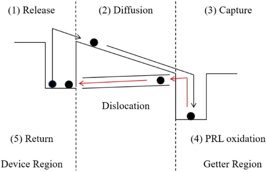 | ||
| Fig. 1 Concept of the PDG process involving release, diffusion, capture, PRL oxidation, and impurities return. | ||
Due to the difference between the thermal expansion coefficient and lattice constant, a large number of dislocations were generated on the surface during the conversion of PRL to PSG, which resulted in the PDG effect being completely negated. In this paper, we added only a small amount of O2 at the end of the PDG process to retain a part of the PRL. In order to remove the PRL, we use a mixture solution of H2O2 and HF. We judge whether PRL and PSG are removed completely by the hydrophobicity of the surface,16 and change the concentration of H2O2 to select the best solution ratio. The wet chemical method using the solution is a “gentle” method of removal. Lattice mismatches are released before they accumulate into dislocations.
2. Experiments and methods
Even though the most efficient silicon solar cells are N-type, the current PV market is still overwhelmingly P-type.1 The samples used in all experiments are untreated P-type c-Si with a sheet resistance of 0.75 Ω sq−1, the thickness of 170 μm, and the size of M10 (182 mm × 182 mm) from Longi Green Energy Technology Co., Ltd., Xi'an, Shanxi, China.2.1. Thermal oxidation
Before the wet oxidation experiment, we designed the traditional thermal oxidation PDG experiment I. Experiment I is designed with the different gettering processes and a control group. We use B and P as the source of the getter.5–8 The process in this work is outlined in Fig. 2, the first group (S1) only performs PDG, the second group (S2) with BDG and PDG, the third group (S3) only performs BDG, and the fourth group as the control group (S4) does not perform the process of gettering. In the experiment, each group has 30 pieces.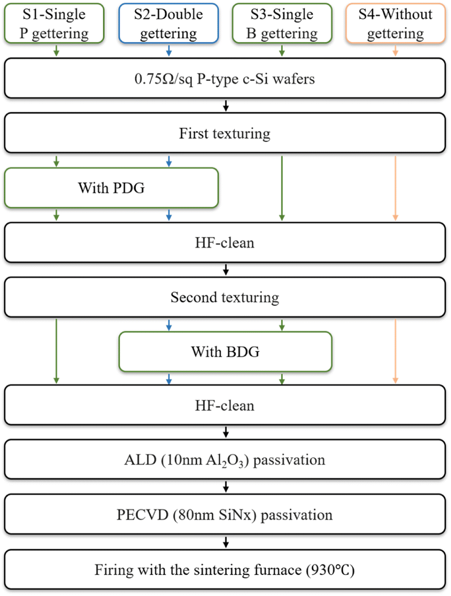 | ||
| Fig. 2 The specific process of experiment I. | ||
As for PDG, samples are diffused at 800 °C, and driven-in at 870 °C using the POCl3 source. As for BDG, the samples are diffused at 850 °C, and driven-in at 1000 °C using the BBr3 source. At first, treated with texturing to make the surface better in contact with the getter source. After the first gettering process, HF was used to clean the surface oxide. Then a second texturing begins. This is to remove the impurities trapped by the surface getter layer and erase the influence of the previous getter source during the second gettering process. The second texturing also be performed for S4, the thickness of all samples is consistent. The passivation structure was prepared after gettering treatment. Atomic layer deposition (ALD) and plasma-enhanced chemical vapor deposition (PECVD) were used to grow the layers of 10 nm Al2O3 and 80 nm SiNx on double sides of the sample, respectively.
After firing with the sintering furnace, we measuring the performance of total samples by quasi steady-state photo-conductance (QSSPC, Sinton WCT-120).17 A sensor (a coil built into the instrument stage) is placed near the sample and sends electromagnetic waves into the silicon light (1 sun) is then pulsed onto the sample to create the excess carriers, and the coil circuit senses the increase in conductance of the sample due to the carriers. We test four corners and the central position of each piece, and the average value obtained from the test is regarded as the test result. Lifetime, J0, implied open-circuit voltage (i-VOC) and implied fill factor (i-FF) are listed in Table 1 of experiment I.
| Lifetime (μs) | J0 (fA cm−2) | i-VOC (mV) | i-FF (%) | |
|---|---|---|---|---|
| S1 | 524.0 | 6.4 | 707 | 83.39 |
| S2 | 654.6 | 16.7 | 708 | 83.79 |
| S3 | 464.5 | 15.3 | 704 | 83.21 |
| S4 | 324.1 | 4.8 | 706 | 82.14 |
According to the results in Table 1, S2 with PDG and BDG is good at lifetime, i-VOC, and i-FF and it is easy to explain that the gettering process improves the performance of the samples. But there is a difference with the result of J0. We interpret the result as follows. According to references,18,19 minority carrier lifetime of the device (τeff) depends on bulk (τbulk) and surface (τsurf) recombination:
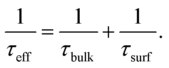 | (1) |
Combining with the data and summary results in Table 1, it is not difficult to see that getter can effectively improve the τeff and τbulk of the device, but also lead to the deterioration of surface performance. In Fig. 1, this process is shown in the gettering process the impurities in the bulk region are “enriched” to the surface. When the getter layer is removed, the impurities are not completely removed, which deteriorates the surface region. Due to the dislocation mentioned above and the impurities return, the impurities on the surface are more concentrated than before gettering. But for the whole sample, the impurities concentration is reduced. As a result, τbulk is greatly increased, in contrast, τsurf is slightly reduced. According to (1), the result of τeff is still increased, which is consistent with the result of Table 1. In each gettering, the lifetime increase, but J0 decrease.
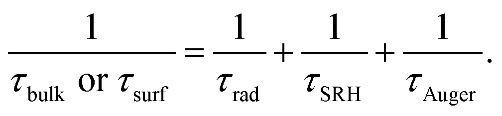
As follows, the τbulk or τsurf, depends on the Shockley–Read–Hall recombination (τSRH), band-to-band radiative recombination (τrad) and Auger recombination (τAuger),19,20
 | (2) |
Among (2), τSRH is closely related to the content of impurities. The less the content of impurities, the smaller the SRH recombination.
2.2. Wet oxidation
In order to improve the gettering effect as much as possible, it is necessary to design a new method so that the impurities will not be returned to the wafer after being “captured”. The return of impurities mainly occurs in the process of PRL oxidation to PSG. Therefore, we designed experiment II to retain a part of PRL in the PDG and use wet oxidation to “gently” remove PRL. The process of experiment II flow is outlined in Fig. 3(a). Experiment II consisted of the control group SP1 without PDG, the conventional thermal oxidation group SP2, and the wet oxidation series SP3. Because SP2 and SP3 are used different PDG recipes, to avoid the influence of doping on τbulk calculation, the sheet resistance is kept at 55–60 Ω sq−1.21,22 Each group is also set with 30 pieces.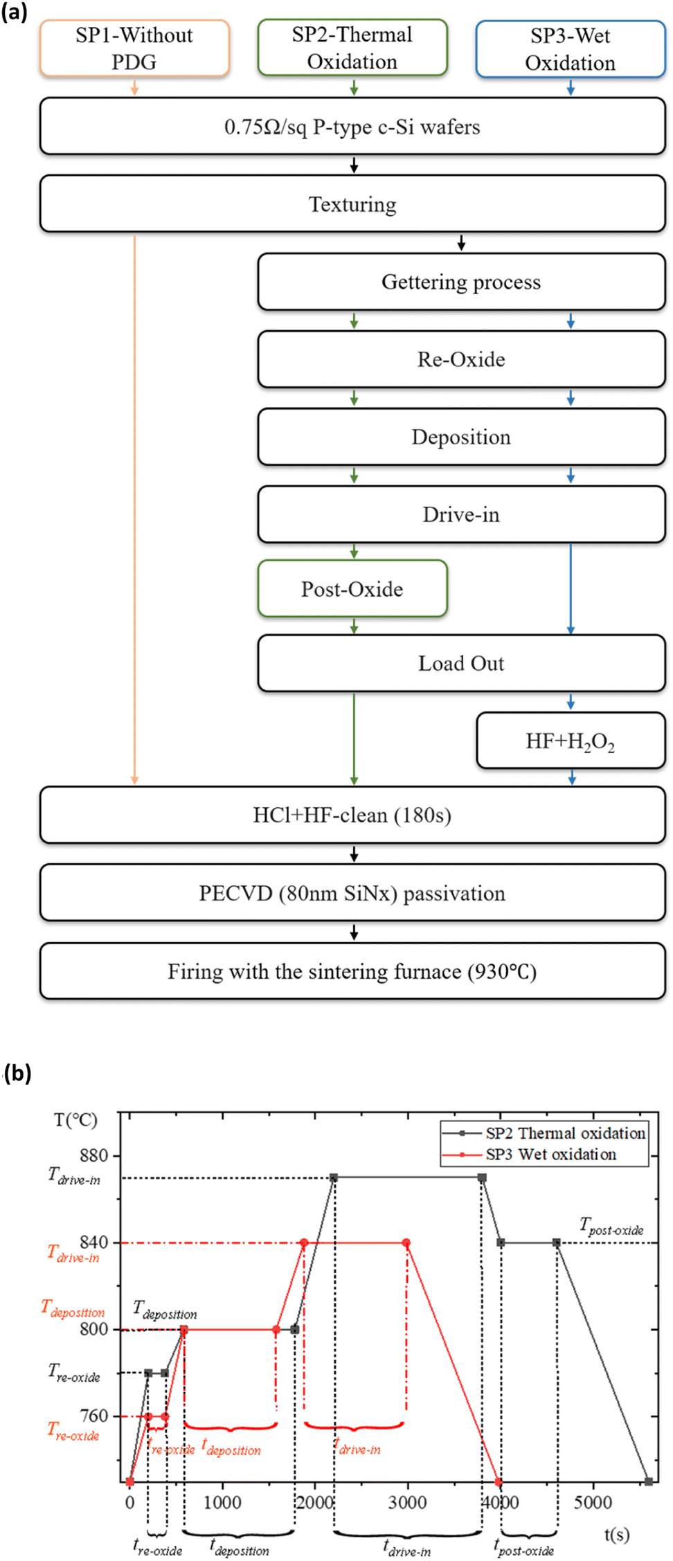 | ||
| Fig. 3 (a) The specific process of experiment II. (b) The doping recipes of SP2 and SP3. | ||
The getter source used in experiment II is also POCl3, which is decomposed into PCl5 and P2O5 at a high temperature great than 600 °C. The reaction equation is:23
 | (3) |
Then, P2O5 reacts with the silicon atoms on the surface of the wafer at the diffusion temperature to form SiO2 and P atoms:
| 2P2O5 + 5Si = 5SiO2 + 4P↓. | (4) |
It can be seen from (3) that the POCl3 is insufficient when it is thermally decomposed, resulting in the formation of PCl5 which is not easily decomposed. Therefore, in the process of deposition, a certain amount of O2 is generally required to promote the further decomposition of PCl5 into P2O5 and the release of Cl2. The reaction equation is:23,24
 | (5) |
According to (4), the generated P2O5 further interacts with silicon atoms and finally forms PRL. Therefore, total PRL cannot be retained. Compared with SP2, SP3 omit the post-oxide process, but certain O2 must be fed into the deposition process to promote the complete decomposition of POCl3. (4) and (5) must occur at high temperatures. Under this condition, O2 dissociates into a single atom since the radius of the O(Si) is smaller than that of the Cl(P), the former will be more oxidizing Cl− can be oxidized to Cl. The situation in (4) is similar. The doping recipes of SP2 and SP3 are shown in Fig. 3(b), where T and t stand for degree centigrade (°C), and second (s).
SP3 removes PRL and PSG by wet oxidation with a mixture solution of H2O2 and HF after the end of the diffusion process. SP3 is further divided into five different groups SP3-1, 2, 3, 4, and 5 according to the different concentrations of H2O2 oxidant used.25,26 In total groups, the proportion of HF remained unchanged, accounting for 10%. The proportion of H2O2 in SP3-1 is 20% and increases by 5% in each group until the content of H2O2 in SP3-5 reaches 40%. The rest of the solution is DI water (Deionized water). Total groups were equipped with the monitor that used alkali (KOH) polishing as the source of surface characterization information. To facilitate the 3D optical microscope measure the surface morphology information. The concentration of chemical reagents HF, HCl, and KOH are all 45 wt%, H2O2 is 30 wt% the purity is chemical pure (CP) from Kunshan Fuller Chemical Co., Ltd., Soochow, Jiangsu, China. The proportions in this paper are all volume ratios (%).
After oxidation, total samples (including the SP1 and SP2) are cleaned for 180 s with the solution of 10% HCl and 25% HF. Cl− can combine with metal ions to form the complex, thereby metal impurities from the wafer surface are thorough.27–29 We test the sample by electrochemical capacitance–voltage (ECV) profiling. And test the monitor with a 3D optical microscope. PECVD is used to grow the layer of 80 nm SiNx on double sides of the total samples as the passivation layer. After firing with the sintering furnace we measuring the performance of total samples by Sinton WCT-120 and photoluminescence (PL). The PL test should be carried out first, and other tests should be carried out to avoid the influence of sample scratches on the PL test results. PL uses a light source with the wavelength of 918 nm and a working light intensity of 1 sun in this paper.
Moreover, wet oxidation at room temperature is undoubtedly more economical than thermal oxidation at high temperature. To verify whether the wet oxidation process can be easily introduced into the production line, and improve the efficiency of wet oxidation, at the end of experiment II, we selected the group with the best performance in the SP3, and compare the PCE.
3. Results and discussion
3.1. Thermal oxidation
Lifetime (τeff), J0, i-VOC, and i-FF are shown in Fig. 4 of experiment II.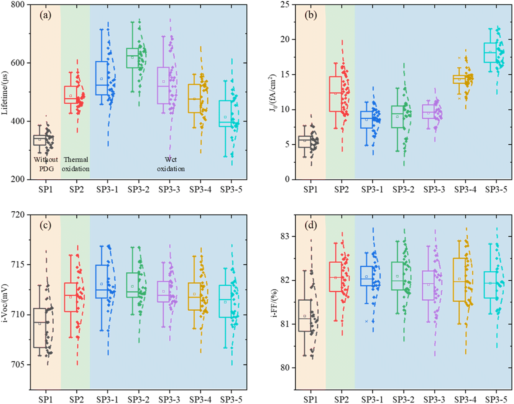 | ||
| Fig. 4 Sinton test results of the experiment II, (a) lifetime (τeff), (b) J0, (c) i-VOC, (d) i-FF. | ||
It can be seen that the surface of c-Si solar cells can be effectively modified by the method of wet oxidation. In Fig. 4(b), it can be found that, although the surface of SP2 and SP3 is still worse than that of the SP1 group without a getter, which we have explained before, parameter J0 in 1, 2, and 3 of SP3 are smaller than SP2. Due to the surface modification by wet oxidation, the gettering effect is further improved. It shows that the lifetime of SP3-2 is 26.3% higher than that of SP2, about 132 μs.19,20
3.2. Surface region
The sample has also been subjected to the PL to test the quality of the overall region of the device. Representative PL images of each group are selected and shown in Fig. 5.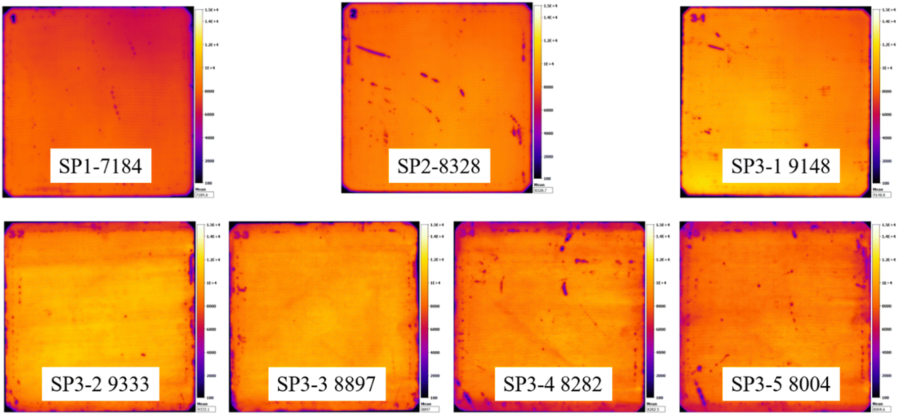 | ||
| Fig. 5 PL images of each group (exposure time is 0.3 s). | ||
The PL images further prove that wet oxidation can significantly improve the gettering effect, but with the increase of H2O2 concentration, the brightness of images becomes more and more uneven it is because that wafer is etched and the reaction products are H2O, dissolved Si (H2SiF6), and possibly O2 from the decomposition of H2O2 (6):
| Si + H2O2 + HF → H2SiF6 + H2O. | (6-1) |
| 2H2O2 → 2H2O + O2. | (6-2) |
H2O2 as an unstable oxidant is very easy to decompose in the chemical reaction and will produce a large number of bubbles.30,31 This is why we see obvious “waves” on images in groups with a high concentration of H2O2.
In experiment II, each group is set with the monitor. We observe the surface structure of each group with the 3D optical microscope as shown in Fig. 6.
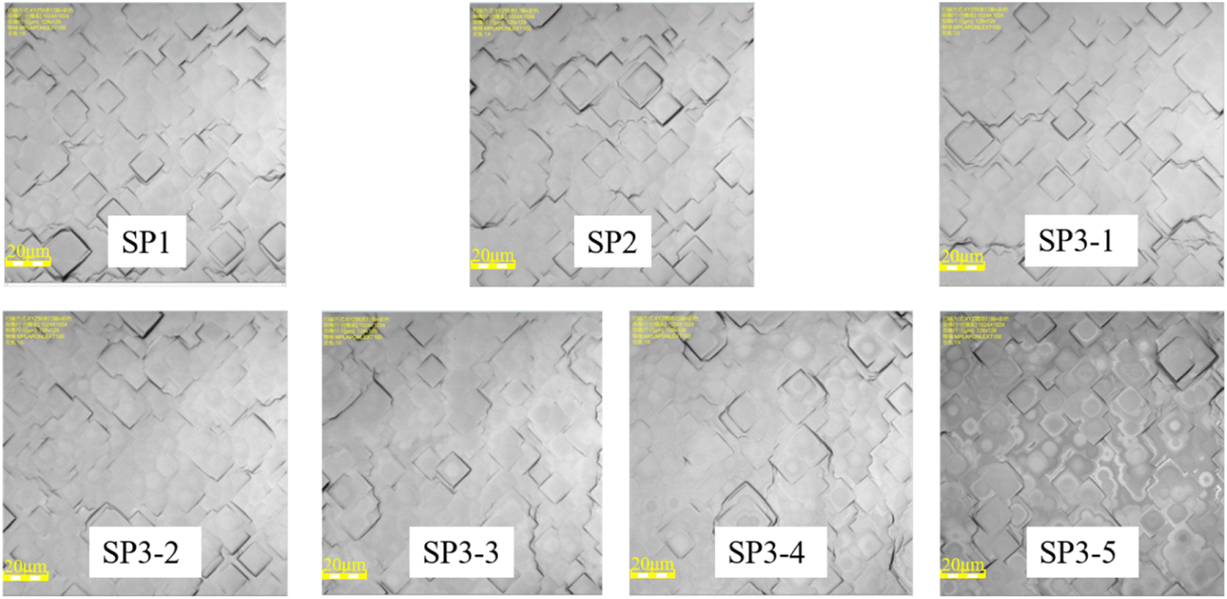 | ||
| Fig. 6 Results of 3D optical microscope observation. | ||
The results show that H2O2 with high concentration, causes some corrosion on the wafer surface, and it is no longer smooth. In the group SP3, a certain amount of etch pits is observed. The higher the concentration of H2O2, the greater the density of etch pit. This is also the reason for the deterioration of the properties of the high concentration group in SP3. In Fig. 4(a) and (b), with the increase of concentration H2O, at first, the recombination region becomes larger, next the J0 increases, and at last, the gettering effect is canceled. This result makes the lifetime of wet oxidation worse than that of the thermal oxidation group,32 lifetime of SP3-5 is 14.3% lower than that of SP2, about 72 μs.
3.3. Bulk region
The significance of the wet oxidation method is that it can improve the removal of impurities in the gettering process and the quality of silicon wafers. Therefore, we compare the performance of the bulk region of two getter methods by calculation. We take the minority carrier lifetime in the bulk region (τbulk) as the standard. We show the calculation method of τbulk in33
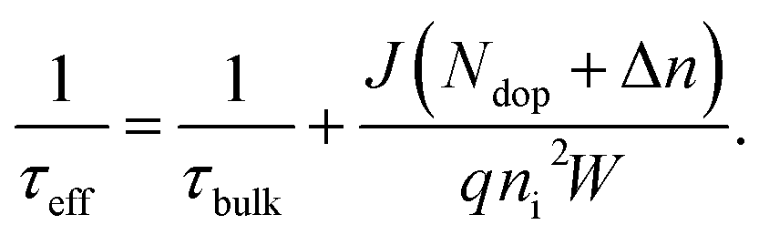 | (7) |
Among (7), Ndop is intrinsic doping concentration, and the value is 5E15 cm−3. Δn is excess carrier concentration, and the value is 1E15 cm−3. q is the amount of electron charge, and the value is 1.6 × 10⁻¹⁹ C. ni is the intrinsic carrier concentration of silicon, and the value is 8.6 × 109 cm−3. W is the thickness of the wafer, and the value is 170 μm. Here J refers to the sum of J0,front, and J0,rear, the sample has a symmetric structure, and the data of J0 in Fig. 4(b) can be directly used.
The dopant diffusion profiles of each group sample are by using ECV to calculate the τbulk.
In Fig. 7, there is almost no difference in the dopant diffusion profiles of each group which indicate that the influence of doping concentration can be negligible on τbulk. In Fig. 7(b), we can see that the ECV test results of total SP3 samples processed in the same tube are significantly different in the 0–10 nm. This further validates Sinton's results in Fig. 4. With the appropriate of doping concentration, i-VOC increases.34 However, H2O2 with high concentration etches the surface thickness 0–10 nm, and the i-VOC of each group of SP3 in Fig. 4(c) show a changing trend of first increasing and then decreasing.
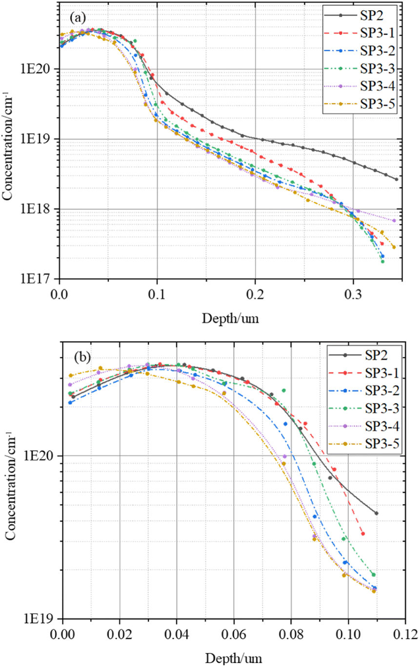 | ||
| Fig. 7 The dopant diffusion profiles of each group samples, (a) 0–0.35 μm, (b) 0–100 nm. | ||
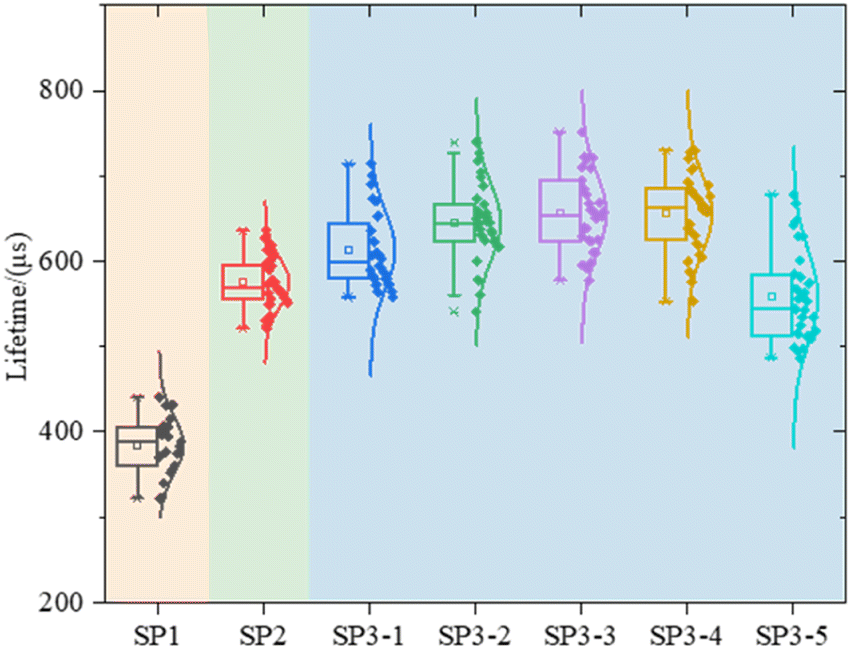
After that, we calculate τbulk according to (7). The data in Fig. 8 further indicates that the τbulk of SP3-4 in the wet oxidation group is 14% higher than that of SP2, about 81 μs. Combining the information in Fig. 4–8, although thermal oxidation can improve the values of τeff, the gettering effect is negated by the deterioration of the surface. Therefore, there should be a compromise between surface and bulk, and the compromise is wet oxidation. Although the surface will eventually be damaged due to the factors of principle wet oxidation with appropriate solution concentration can improve the performances of the bulk region thus the performances of the whole device are improved.
 | ||
| Fig. 8 The calculated result of τbulk. | ||
3.4. Cell manufacturing
In experiment II, we believe that the group SP3-2 is the champion considering the surface and bulk region. The SP3-2 recipe is introduced into the existing production line equipment then we compare the PCE for traditional oxidation.In silicon solar cell manufacturing, the emitter is prepared by diffusion process.17 Nevertheless, the diffusion process will cause of wrap-around, which would cause a short circuit in the final solar cell. Therefore, at the end of the diffusion process, the single sided etching process is implemented to remove the diffused rear side region. In the solar cell, it's so-called “edge isolation”.
The RENA InOxSide machine and classic acidic with a mixture of HF/HNO3 are used for the thermal oxidation group to edge isolation. The rear side is treated the same way for the wet oxidation group. Wafer only needs to go through the etch bath. And the water wheel automatically turns the equipment into the “wet oxidation bath”. In the wet oxidation bath, PRL and PSG are removed, and the process is about 170 s. Then carry out HF/HCl rinse bath, and the remaining oxide is removed from the surface. The results show that compared with the traditional “thermal oxidation and etching”, the wet oxidation process is introduced into the existing production line only by adding automatic turning equipment, and H2O2 consumption needs 86 L/10![[thin space (1/6-em)]](https://www.rsc.org/images/entities/char_2009.gif) 000 pieces. However, it can be seen from Fig. 3(b) that wet oxidation can reduce 1100 s of the recipe time. At thermal oxidation, the heating power is generally 60–80 kW, and the constant temperature power is 25–30 kW for the furnace tube in industrial production. Its production capacity is generally 1000–1500 pieces per tube. In contrast, the transmission power of the inline machine in wet oxidation is only 1.5–2.5 kW, the speed is 3–4 m min−1, and it usually has five tracks at least. For the processing of 10000 M10 silicon wafers as a comparison. Thermal oxidation will consume about 65 kW h more electric energy. Moreover, the price of CP H2O2 used in industrial production of wet oxidation is very low, it is only about US$ 0.09 per L. Taking into account the additional use of gases such as O2 in thermal oxidation, wet oxidation becomes more advantageous.
000 pieces. However, it can be seen from Fig. 3(b) that wet oxidation can reduce 1100 s of the recipe time. At thermal oxidation, the heating power is generally 60–80 kW, and the constant temperature power is 25–30 kW for the furnace tube in industrial production. Its production capacity is generally 1000–1500 pieces per tube. In contrast, the transmission power of the inline machine in wet oxidation is only 1.5–2.5 kW, the speed is 3–4 m min−1, and it usually has five tracks at least. For the processing of 10000 M10 silicon wafers as a comparison. Thermal oxidation will consume about 65 kW h more electric energy. Moreover, the price of CP H2O2 used in industrial production of wet oxidation is very low, it is only about US$ 0.09 per L. Taking into account the additional use of gases such as O2 in thermal oxidation, wet oxidation becomes more advantageous.
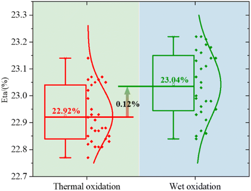
After the passivation layer, we screen-print the Al finger grid on the rear side as the metal electrode. The silver (Ag) finger grid is printed on the front side of an electrode. All samples are manufactured into P-PERC cells (P-type Passivated Emitter and Rear Cell). We compared the PCE of the two methods. The results are shown in Fig. 9. The test results indicate that in small batch manufacturing, the PCE of wet oxidation will increase by about 0.12%. This is further evidence that the wet oxidation method proposed enhances the gettering effect and removed more metal impurities. In the subsequent wet oxidation process, the weak oxidizing H2O2/HF mixture is used to oxidize and remove PRL and PSG, preserving the front side pyramid structure as much as possible.
 | ||
| Fig. 9 The PCE results of thermal/wet oxidation. | ||
Although wet oxidation will cause some damage to the surface. But it can be seen from the results in Fig. 6 and 7 that the damage is minimal. We test by the EL (electroluminescence, EL uses direct current, voltage is 16 V, current is 6 A), it is found damage on the edge of some samples (Fig. 10). This may be due to the failure of the water film protection. And the bubbles are caused by H2O2 decomposition, a part of the solution is splashed to the edge of the wafer. Because wet oxidation is applied to the front surface, the rear surface was hydrophobic. Cause the edge of the wafer is etched for H2O2. But, H2O2 oxidation is weak, even in the case that the water film cannot fully protect, it will only affect the edge region. From the results of PCE, the gain is greater than the damage. Even though wet oxidation will bring additional damage to edge etch compared to thermal oxidation with mature technology, the final result can still improve the PCE.
 | ||
| Fig. 10 EL images of thermal/wet oxidation. | ||
4. Conclusions
Combined the discussion in this paper, shows that the getter is very effective at removing impurities. However, oxidizing the PRL to PSG thermally will release the captured impurities back into the wafer. Hence the gettering effect is negating. We propose a new method, surface modifications by wet oxidation method removing getter layer. In the process of PRL removal by oxidation, a little of Si will always be etched, causing some damage to the surface, but provided the appropriate ratio of solution concentration is selected, more impurities can be removed and gettering effect can be improved on the premise of reducing the surface damage as much as possible. Wet oxidation of the PDG method, not only can be used as a getter means to improve the performances of wafers, through the ECV results, but it can also be integrated into the cell manufacturing process, as an n+ emitter preparation method. Comparing the PCE of the two kinds of cells, it was found that the efficiency of the wet oxidation cell was significantly improved. These results are useful in developing suitable high-efficiency c-Si solar cells.Conflicts of interest
There are no conflicts to declare.Acknowledgements
This paper would like to thank Engineer G. H. Ji for guidance and suggestions, Engineer J. Bao for fruitful experiences of theoretical knowledge, and Engineer C. Chen for familiar with wet chemical equipment. Dr S. W. Sim and Dr Z. R. Du are familiar with English and have assisted in the experiments and writing. Engineer J. N. Yang assisted in the diffusion part of the experiment. Engineer J. T. Jiang and C. P. Chen assisted in the passivation part of the experiment. Engineer C. Huang and Q. Wang guide the use of the characterization equipment. L. Chen communicated with the other departments. Finally, F. A. author would like to express special thanks to his friend Dr D. Ding from Shanghai Jiao Tong University, China, who has taught him a lot about solar technology.References
- International Technology Roadmap for Photovoltaic (ITRPV), 2021, https://itrpv.vdma.org/web/itrpv/download Search PubMed.
- R. Basnet and F. E. Rougieux, et al., IEEE J. Photovolt., 2018, 8, 990–996 Search PubMed.
- S. P. Phang and W. Liang, et al., IEEE J. Photovolt., 2013, 3, 261–266 Search PubMed.
- A. Liu and Z. H. Yang, et al., Sol. Energy Mater. Sol. Cells, 2021, 230, 111254 CrossRef CAS.
- T. E. Seidel, R. L. Meek and A. G. Cullis, J. Appl. Phys., 1975, 46, 600–609 CrossRef CAS.
- J. S. Kanga and D. K. Schroder, J. Appl. Phys., 1989, 65, 2974–2985 CrossRef.
- A. Haarahiltunen and H. Talvitie, et al., Appl. Phys. Lett., 2008, 92, 021902 CrossRef.
- S. P. Phang and D. Macdonald, J. Appl. Phys., 2011, 109, 073521 CrossRef.
- O. Schultz, S. W. Glunz, S. Riepe and G. P. Willeke, Prog. Photovoltaics, 2006, 14, 711–719 CAS.
- D. Abdelbarey, V. Kveder, W. Schröter and M. Seibtb, Appl. Phys. Lett., 2009, 94, 061912 CrossRef.
- S. Dubois and T. Turmagambetov, et al., Sol. Energy Mater. Sol. Cells, 2016, 157, 558–564 CrossRef CAS.
- B. Lai and H. Shen, et al., Sol. Energy, 2021, 222, 230–234 CrossRef CAS.
- K. Adamczyk and R. Søndena, et al., J. Appl. Phys., 2018, 123, 055705 CrossRef.
- A. Zarroug, Z. Hamed, Z. B. Hamed, L. Derbali and H. Ezzaouia, J. Cryst. Growth, 2017, 463(1), 95–99 CrossRef CAS.
- M. Rinio and A. Yodyungyong, et al., Phys. Status Solidi A, 2011, 208, 760–768 CrossRef CAS.
- J. W. Leem and S. H. Lee, et al., Adv. Energy Mater., 2014, 4, 1301315 CrossRef.
- R. A. Sinton, A. Cuevas and M. Stuckings, Proc. 25th Photovoltaic Specialists Conference, 1996, pp. 457–460 Search PubMed.
- R. L. Milot and R. J. Sutton, et al., Nano Lett., 2016, 7001–7007 CrossRef CAS PubMed.
- E. Aydin and M. D. Bastiani, et al., Adv. Mater., 2019, 31, 1900428 CrossRef PubMed.
- F. Staub and H. Hempel, et al., Phys. Rev. Appl., 2016, 6, 044017 CrossRef.
- M. K. Basher and M. J. Uddin, et al., Mater. Res. Express, 2019, 6, 085510 CrossRef CAS.
- M. Chen and R. H. Zha, et al., Chem. Eng. J., 2017, 313, 791–800 CrossRef CAS.
- S. Amin and M. M. Alam, et al., Phosphorus, Sulfur Silicon Relat. Elem., 2020, 196, 211–274 CrossRef.
- H. Z. Li and K. Kim, et al., Front. Energy, 2016, 42–51 Search PubMed.
- A. Stapf, F. Honeit, C. Gondek and E. Kroke, Sol. Energy Mater. Sol. Cells, 2017, 159, 112–120 CrossRef CAS.
- H. X. Lai and L. Q. Huang, et al., Hydrometallurgy, 2016, 164, 103–110 CrossRef CAS.
- A. Moldovan and K. Birmann, et al., Solid State Phenom., 2012, 195, 305–309 Search PubMed.
- A. Azizitorghabeh, F. Rashchi and A. Bakakhani, Sep. Purif. Technol., 2016, 171, 197–205 CrossRef CAS.
- Z. J. Hu and T. Zhang, et al., Sep. Purif. Technol., 2021, 272, 118822 CrossRef CAS.
- C. Chartier, S. Bastide and C. Lévy-Clément, Electrochim. Acta, 2008, 53, 5509–5516 CrossRef CAS.
- C. Gondek and M. Lippold, et al., J. Phys. Chem. C, 2014, 118, 2044–2051 CrossRef CAS.
- P. H. Ren and C. F. Sun, et al., J. Mater. Chem. C, 2019, 7, 1934–1947 RSC.
- D. Macdonald, R. A. Sinton and A. Cuevas, J. Appl. Phys., 2001, 89, 2772–2778 CrossRef CAS.
- K. Hirata and T. Saitoh, et al., Appl. Phys. Express, 2011, 5, 016501 CrossRef.
| This journal is © The Royal Society of Chemistry 2023 |