
 Open Access Article
 This Open Access Article is licensed under a
 Creative Commons Attribution 3.0 Unported Licence
Experimental verification of SO2 and S desorption contributing to defect formation in MoS2 by thermal desorption spectroscopy†
Shuhong
Li
ab,
Tomonori
Nishimura
a,
Mina
Maruyama
b,
Susumu
Okada
 b and
Kosuke
Nagashio
*a
b and
Kosuke
Nagashio
*a
aDepartment of Materials Engineering, University of Tokyo, Tokyo 113-8656, Japan. E-mail: nagashio@material.t.u-tokyo.ac.jp
bDepartment of Physics, University of Tsukuba, Tsukuba, Ibaraki 305-8577, Japan
First published on 28th November 2022
Abstract
The defect-free surface of MoS2 is of high importance for applications in electronic devices. Theoretical calculations have predicted that oxidative etching could be responsible for sulfur vacancy formation. No direct experimental evidence, however, points out the role of adsorbed oxygen on sulfur vacancy formation for MoS2, especially on an insulating SiO2/Si substrate. Herein, by applying thermal desorption spectroscopy, we found that sulfur loss can be tightly coupled to adsorbed oxygen, as confirmed by observation of SO2 desorption. With annealing MoS2, even under ultrahigh vacuum, oxygen molecules adsorbed on MoS2 assist the sulfur atom in dissociating from MoS2, and thus, defects are formed as the result of SO2 desorption from 200 °C to 600 °C. At higher temperatures (over 800 °C), on the other hand, direct sulfur desorption becomes dominant. This finding can be well explained by combining the morphology investigation enabled by atomic layer deposition at defective sites and optical transitions observed by photoluminescence measurements. Moreover, a preannealing treatment prior to exfoliation was found to be an effective method to remove the adsorbed oxygen, thus preventing defect formation.
1. Introduction
MoS2, a two-dimensional (2D) layered material, is promising as a channel material for next-generation field-effect transistors (FETs) because a natural thin body can overcome the scaling limit for the Si gate length.1,2 Although the dangling-bond-free surface of the layered MoS2 channel is expected to ideally provide an electrically inert interface, sulfur vacancies in reality have been recognized as a dominant defect in MoS2 due to the lowest formation energy of ∼1.3–1.5 eV under S-poor conditions.3,4 Moreover, sulfur vacancies are known to introduce defect states in the band gap, which degrades the FET performance.5–8 Therefore, controlling sulfur vacancies has still been an critical issue due to the limited understanding of its formation mechanism, even though many healing processes based on various adsorbates or S vapor annealing have been proposed.9–12The stability of MoS2 has been intensively studied thus far.13,14 The conventional mechanical exfoliation process for device fabrication leads to exposure to ambient air, which introduces adsorbates on the MoS2 surface and edge. These adsorbates, such as oxygen and water, greatly affect chemical stability, since thermodynamic calculations suggest that most 2D materials show oxidation tendencies.15 The long-term exposure of MoS2 flakes to ambient air has proven the gradual oxidation from the edges to the interior of MoS2![[thin space (1/6-em)]](https://www.rsc.org/images/entities/char_2009.gif) 16 because the coordinatively unsaturated edge is energetically more favorable for oxidation than the basal plane.17–20 For intentional exposure to an oxygen environment,21 the basal plane of MoS2 is oxidized, and MoO3 is formed during oxidation above 400 °C. This is further supported by the aggressive oxidation using oxygen plasma, where layer-by-layer oxidation was observed since MoO3 formed on the MoS2 surface prevented further oxidation.22 Interestingly, for an oxygen/air environment at lower temperatures of 300–340 °C, however, layer-by-layer anisotropic etching of MoS2 results in triangular pits, which are initiated via intrinsic defects on the basal plane of MoS2.21,23 This oxidative etching is explained by the reaction of MoS2 + O2 → MoO3↑ + SO2↑,18,24 where both MoO3 and SO2 are volatile. Thus, oxidative etching is considered to be an important process when MoS2 is exposed to oxygen or air.
16 because the coordinatively unsaturated edge is energetically more favorable for oxidation than the basal plane.17–20 For intentional exposure to an oxygen environment,21 the basal plane of MoS2 is oxidized, and MoO3 is formed during oxidation above 400 °C. This is further supported by the aggressive oxidation using oxygen plasma, where layer-by-layer oxidation was observed since MoO3 formed on the MoS2 surface prevented further oxidation.22 Interestingly, for an oxygen/air environment at lower temperatures of 300–340 °C, however, layer-by-layer anisotropic etching of MoS2 results in triangular pits, which are initiated via intrinsic defects on the basal plane of MoS2.21,23 This oxidative etching is explained by the reaction of MoS2 + O2 → MoO3↑ + SO2↑,18,24 where both MoO3 and SO2 are volatile. Thus, oxidative etching is considered to be an important process when MoS2 is exposed to oxygen or air.
Recently, atomic-resolution scanning tunneling microscopy (STM) suggested that the O2 adsorbed on the basal plane of MoS2 volatized as SO2 by removing S, leaving S vacancies with O saturation on the basal plane.10 This O2-assisted S vacancy formation in ambient air at room temperature (RT) is estimated to be energetically spontaneous with −0.49 eV by first principles calculation. On the other hand, in a high vacuum environment, the creation of S vacancies has been confirmed not at 127 °C but at elevated temperatures >627 °C by atomic-resolution STM25 and transmission electron microscopy (TEM).26 These results indicate that the formation of S vacancies at RT cannot be fully explained without the existence of oxygen adsorbed on the basal plane of MoS2, suggesting the importance of O2 adsorption and reaction mechanism. Therefore, further theoretical studies on the initial step of oxidative etching have been conducted in detail.27 However, direct experimental evidence of SO2 desorption as well as direct S desorption has not yet been proven.
Here, thermal desorption mass spectrometry (TDS) is used to study the surface reaction and desorption kinetics in Si28,29 Ge,30 and HOPG31 by detecting a small amount of desorption species using a quadrupole mass spectrometer (QMS). By using this TDS system, it may be possible to detect SO2 and/or S desorption from MoS2 flakes transferred onto SiO2/Si substrates in ambient air. Although no measurement method to observe S vacancies with atomic resolution is available for MoS2 on an insulating substrate, it is well known that Al2O3 during atomic layer deposition (ALD) is adsorbed only at the defect sites;32–35 this will allow us to visualize the defect evolution with the assistance of surface topology observed macroscopically by atomic force microscopy (AFM). In this research, a quantitative characterization of the defect evolution mechanism of MoS2 on SiO2 at elevated temperatures up to ∼1000 °C is realized by combining TDS and ALD.
2. Experimental
2H-MoS2 crystals purchased from SPI supplies were used in this study. First, a 110 nm SiO2/n+-Si substrate was sonicated by acetone and isopropyl alcohol for 10 min in laboratory air. After a few exfoliations by metallic tweezers, the bulk MoS2 flakes were directly transferred to the SiO2/n+-Si substrate. This procedure provides a sufficiently large surface area of MoS2 for the TDS measurements, while it prevents any tape residue on the substrate since the tape is not used. Other 2H-bulk transition metal dichalcogenides (WS2, WSe2, MoSe2 and MoTe2) were grown by chemical vapor transport method36 and treated by the same method applied for MoS2. Alternatively, MoS2 flakes were clashed into powders using a mortar to further increase the surface area of MoS2. Then, the MoS2 powders were placed on the SiO2/Si substrate. Fig. 1a illustrates the TDS apparatus, which allows selective heating of only the Si substrate via infrared radiation from the underlying power-operated lamp under ultrahigh vacuum (UHV) conditions of ∼4 × 10⁻⁸ Pa. Since this TDS is cold wall system, the desorption from the inner chamber wall can be avoided during the sample heating. The QMS functions by manipulating the electric field between four orthogonal rods to collect ionized desorbed molecules and atoms and thus enables distinguishing the desorbed species according to its atomic/molecular mass-to-charge ratio. The bulk MoS2 flakes were heated from room temperature to ∼1000 °C with a heating rate of 20 °C min−1, and TDS spectra were detected in multi-ion detection mode with a sensitivity up to 10−15 A.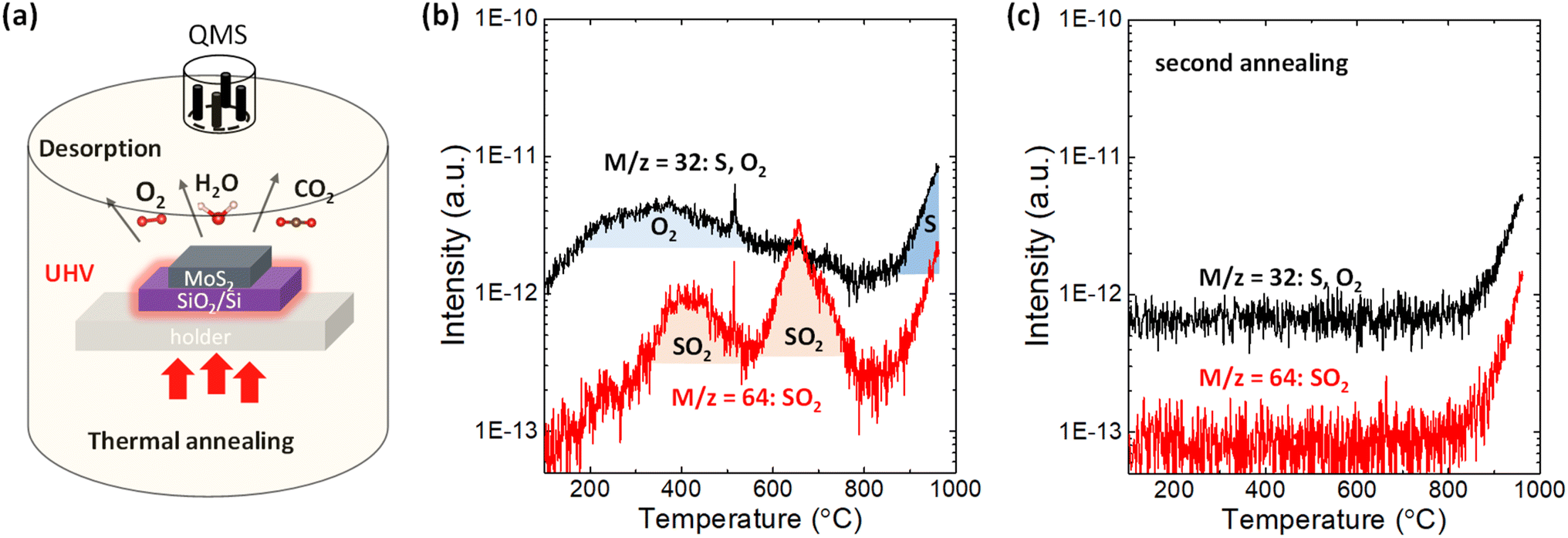 | ||
| Fig. 1 (a) Illustration of thermal desorption spectroscopy applied in this experiment. (b) TDS spectra with m/z = 32 (O2 or S) and m/z = 64 (SO2) for bulk MoS2 flakes on the SiO2/Si substrate. (c) Comparison of the TDS spectra for m/z = 32 between the first annealing and second annealing. | ||
For ALD, Al2O3 was deposited on MoS2 flakes in a hot wall chamber at 200 °C with trimethylaluminum (TMA), water, and nitrogen as the precursor, oxidant, and purge gas, respectively.32 The pulse time for TMA/water is 0.1 s/0.5 s, respectively. Ten cycles were performed to obtain ∼2 nm-thick Al2O3. The surface morphology was measured with dynamic force mode by AFM. The Raman and photoluminescence (PL) spectra were measured at RT in ambient air using a 488 nm excitation laser with a power of 0.06 mW to avoid the degradation of MoS2 owing to laser heating.
3. Results and discussion
First, the desorption of adsorbates on the SiO2/Si substrate without MoS2 flakes should be examined. As shown in Fig. S1a,† in addition to the small amount of H2, CO2 and N2, H2O physiosorbed on the SiO2/Si substrate was clearly detected in the temperature range of 100–300 °C because the SiO2 surface is hydrophilic.37 After transferring MoS2 flakes onto the SiO2/Si substrate, the desorption of H2O and CO2 was enhanced, as shown in Fig. S1b.† This indicates that many kinds of gas species are adsorbed on MoS2 flakes when MoS2 flakes are mechanically transferred in ambient air.The desorption of sulfur and sulfur-related compounds is of the highest interest. Fig. 1b shows the TDS spectra for mass-to-charge ratios of m/z = 32 and 64. S and O2 can be assigned for the same mass-to-charge ratio of m/z = 32 because QMS can only filter substances by mass-to-charge ratio. To separate them, the second annealing experiments were successively carried out without removing the sample, as shown in Fig. 1c and S1c.† The broad peak from 200 to 600 °C for m/z = 32 is totally removed in the second annealing experiment, with the sharp intensity tail remaining at ∼800 °C. It can be expected that direct S desorption is observable even in the second annealing, while O2 is not detected once it has totally desorbed in the first annealing experiment. Therefore, the broad peak from 200 to 600 °C in Fig. 1b is assigned as the contribution from O2. Here, it should be noted that the contribution from water adsorbed to the sample was excluded in this discussion, even though the water desorption was observed in Fig. S1.† According to the recent paper,38 no degradation of monolayer MoS2 was observed after two weeks exposure to the environment of both N2 and N2 with the 75% humidity, suggesting that water itself have no dominant contribution for oxidation. Moreover, the desorption tails observed for all species at a high temperature of ∼800 °C in Fig. S1† basically resulted from the inner pressure enhancement in the TDS chamber, not from the real increase in desorption. Nevertheless, the TDS spectrum of m/z = 32 in the second annealing experiment is greatly enhanced when the surface area of MoS2 increases by preparing the MoS2 powder, which is reflected as a threshold temperature shift to the lower side in Fig. S2a.† This indicates that the desorption tail for m/z = 32 contains real desorption, that is, the contribution from S. Moreover, Fig. S2b† compares the TDS spectra of chalcogens (S, Se and Te) for various transition metal dichalcogenides. The direct Te (m/z = 128) desorption from MoTe2 is stronger than others, which is consistent with the common understanding of the stability of 2D materials.
In addition to direct S desorption, the sulfur oxidation product, that is, SO2, was also observed and expressed as m/z = 64 in Fig. 1b, where two peaks are observed at ∼400 °C and ∼650 °C. It should be noted that the m/z = 64 was assigned to be the SO2 rather than S2 based on the isotope method.39 Sulfur mainly has stable four isotopes: 32S (95.02%), 33S (0.5%), 34S (4.21%), and 36S (0.02%). The second abundant 34S (m = 34) was used to distinguish S2 (m/z = 68) and SO2 (m/z = 66), as shown in Fig. S3(b).† The desorption signal of m/z = 66 well follows m/z = 64, while no clear feature was observed for m/z = 68. Moreover, from the viewpoint of activation energy of S2 desorption, the higher temperature is expected. Therefore, m/z = 64 was assigned to SO2 rather than S2. Furthermore, in the second annealing experiment in Fig. 1c, both peaks disappeared, suggesting that oxygen that constitutes SO2 comes from adsorbates on the MoS2 flakes not from inside of the MoS2 flakes. Therefore, it is considered that adsorbed O2 reacted with S in MoS2 and desorbed as SO2 at ∼400 °C and ∼650 °C. That is, it is suggested that sulfur vacancy formation at relatively low temperature (∼400 °C & 650 °C) is caused by SO2 desorption assisted by oxygen adsorption on the MoS2 basal plane, while it is caused by direct S desorption at high temperature (over 800 °C). Although the theoretical simulation10 has suggested SO2 desorption instead of direct S desorption for S vacancy formation, this is the first experimental observation.
The origin of the two SO2 peaks in Fig. 1b may be related to different intermediates for the final SO2 formation, as suggested in the theoretical calculation.27 The formation of the intermediate “OSOMo”, in which one oxygen atom is inserted into the Mo–S bond, leads to the desorption of SO2 with an energy barrier of 1.49 eV. On the other hand, the formation of the intermediate “Mo–OSO”, which can be seen as the SO2 molecule with one oxygen atom bonded to two adjacent Mo atoms, leads to the desorption of SO and SO2 with energy barriers of 0.41 eV and 0.78 eV, respectively. Interestingly, in the reproduced TDS experiment in Fig. S3,† it is found that the SO signal highly overlaps with the SO2 signal in the low-temperature region, where the first peak is observed in Fig. 1b. The overlapping feature suggests that the formation of SO and SO2 at relatively low temperatures is simultaneous. The slight intense peak for SO at 650 °C can be attributed to the decomposition of SO2 to SO and O due to the ionization in QMS.39 Although the rigorous separation of SO and SO2 is difficult at present, two SO2 peaks may result from the different intermediates for the final SO2 desorption.
To confirm whether defects form as a result of desorption during TDS annealing, 2 nm Al2O3 was deposited by ALD since Al2O3 is formed selectively on defect sites due to the dangling-bond free inert surface of the 2D material.32–35 For the present ALD-assisted morphology characterization, bulk MoS2 were intentionally selected to avoid strain-enhanced ALD growth on monolayer MoS2 due to the transfer process. To show the importance of ALD, the surface topography of MoS2 annealed up to 835 °C in the TDS chamber without ALD was examined to assess the resolution of AFM. As shown in Fig. S4,† no clear defects could be identified. The situation was inverted when ALD was applied to the MoS2 flake after TDS annealing. As shown in Fig. 2b, for the MoS2 flake annealed up to 200 °C in the TDS chamber, the growth of Al2O3 is distributed in dots on the MoS2 surface with a greater concentration at the step edge. It should be noted that 200 °C was selected as the starting temperature for defect characterization since the Al2O3 growth temperature in ALD was 200 °C. As the TDS annealing temperature increases, Al2O3 growth is enhanced, occupying more surface area of MoS2 (Fig. 2b–e). For the MoS2 flake annealed up to 630 °C, the growth of Al2O3 is no longer preferential at the grain boundaries and the step edges but uniformly covers the entire MoS2 surface. The morphology evolution is schematically illustrated below the AFM images.
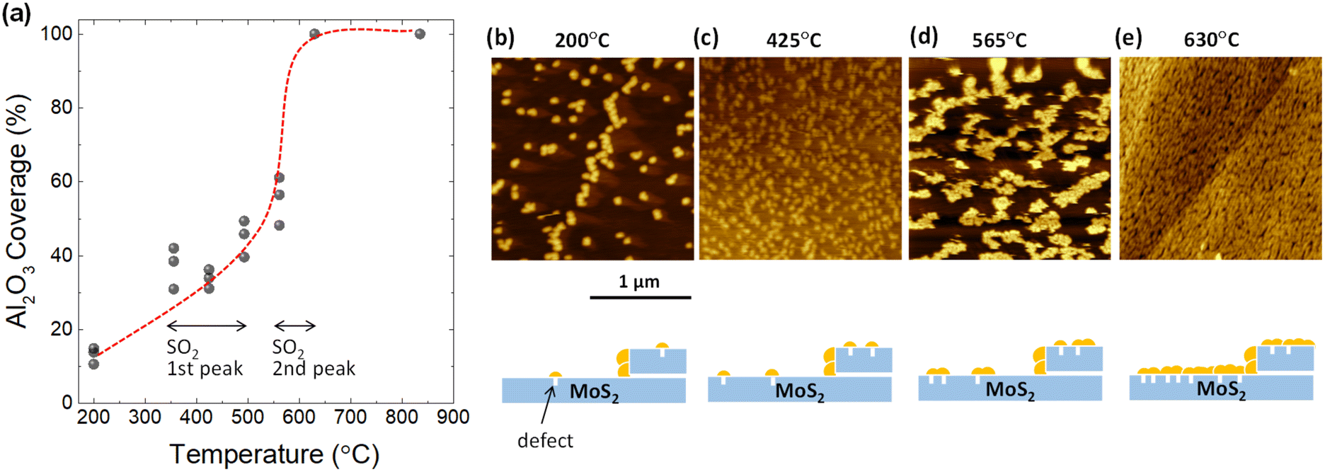 | ||
| Fig. 2 (a) Coverage estimation of ALD-Al2O3 on TDS-annealed bulk MoS2 flakes with varying annealing temperatures. The gray point represents the coverage extracted from different AFM images. The red dashed line is an eye guide to reflect the coverage evolution rate. (b)–(e) Representative AFM images for Al2O3/MoS2 at annealing temperatures of 200 °C, 425 °C, 565 °C, and 630 °C, respectively. In addition, the Al2O3 coverage evolution with increasing annealing temperature is schematically illustrated. The yellow particles represent deposited Al2O3. | ||
Next, the Al2O3 coverage was extracted from the AFM images and plotted as a function of annealing temperature in Fig. 2a. The coverage rate is relatively slow in the temperature range from 350 to 500 °C, where the first peak of SO2 desorption is observed in Fig. 1b. In contrast, there was a significant increase in the coverage rate from 550 to 630 °C. This temperature interval matches the second peak of SO2 desorption. These results suggest that the evolution of the Al2O3 coverage is correlated to SO2 desorption. However, further quantitative estimation of the defect density is not possible here since the Al2O3 particle density does not form a one-to-one correspondence with the defect density. That is, new Al2O3 growth occurs not only at the defect site but also on the Al2O3 that has already been grown. However, the importance of ALD-assisted AFM characterization is to provide clear evidence that the formation of defects on the basal plane of MoS2 flakes does arise when SO2 desorption occurs.
To reveal the structural change in MoS2 after TDS annealing, Raman measurements were conducted. Fig. 3a shows the Raman spectra of monolayer MoS2 at different TDS annealing temperatures. The frequency difference of E12g and A1g is ∼19.4 cm−1, which matches well with the characteristics of monolayer MoS2.40 No detectable shifts of the E12g and A1g peaks were found for any temperature range. On the other hand, the full width at half maximum (FWHM) of these two peaks shown in Fig. 3b is slightly broadened when the annealing temperature was elevated to 835 °C; at this temperature, direct S desorption becomes dominant in the TDS spectra of Fig. 1b. This indicates that some damage to the crystallinity is induced by considerable direct S desorption. The change in Raman spectra at temperatures above 800 °C has also been reported.41 Although Raman spectra are found to be insensitive to temperatures below 630 °C, this is not consistent with Fig. 2a, where a clear Al2O3 coverage evolution is observed. In Fig. S3,† the desorption of SO2 and S was detected but not for MoO, MoO2, and MoO3, suggesting that the original MoS2 crystal lattice can be retained since Mo is located at the center of the MoS2 crystal structure. Therefore, Raman spectra could be insensitive to the relatively small change in crystallinity due to S vacancy formation accompanied by SO2 desorption.
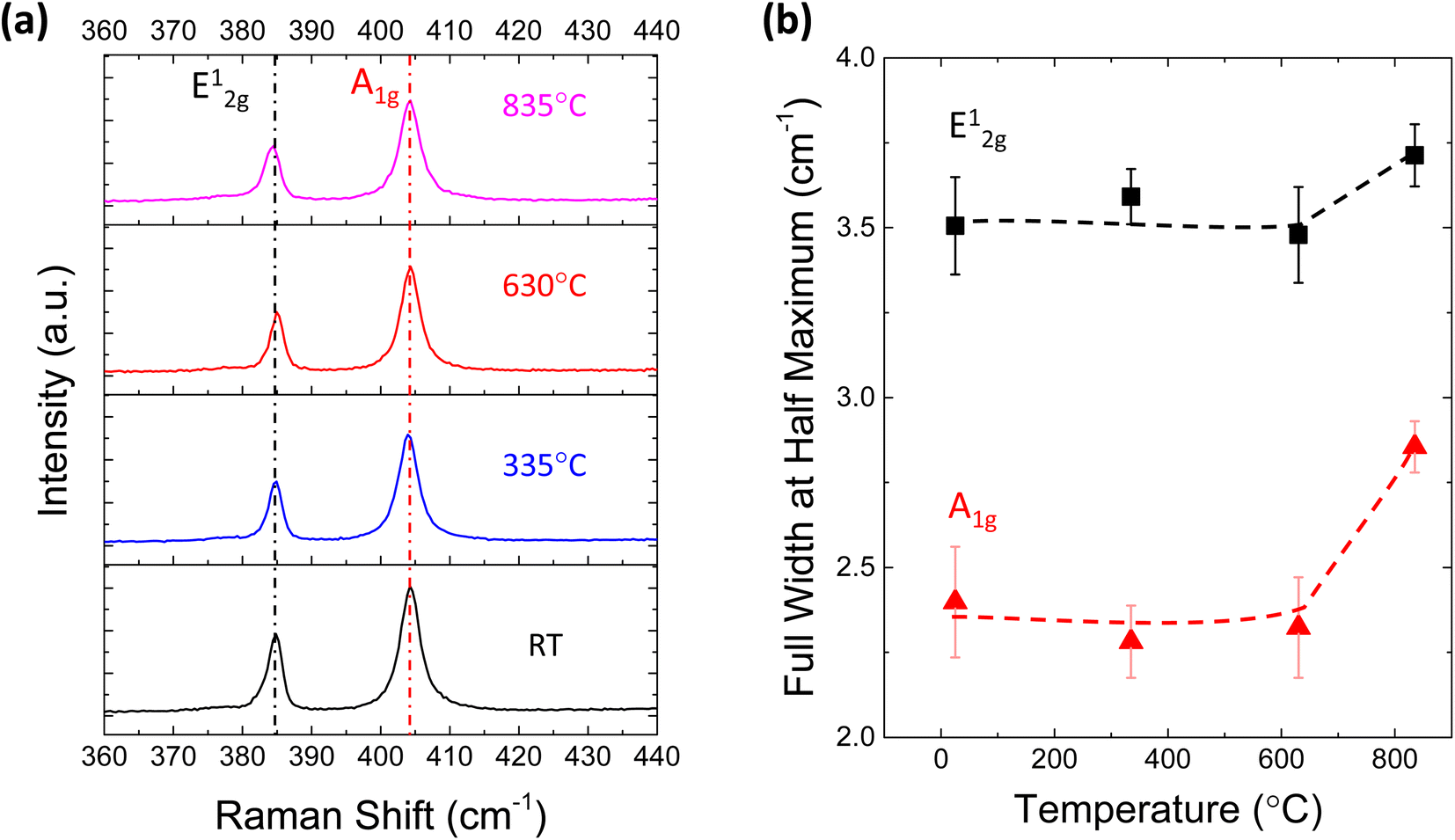 | ||
| Fig. 3 (a) Raman spectra for monolayer MoS2 annealed at different temperatures in the TDS chamber. (b) Full width at half maximum (FWHM) of the Raman peaks at different temperatures. | ||
To further investigate the effect of defect formation more sensitively, PL measurements were performed for monolayer MoS2 annealed at different temperatures in the TDS chamber. As shown in Fig. 4a, the conventional broad PL peak mixed with exciton (X, ∼1.9 eV) and trion (X−, ∼1.85 eV) was observed.42–44 As the TDS annealing temperature increased from RT to 630 °C, the intensity of the exciton peak drastically increased. Since the MoS2 flakes were exposed to ambient air during the PL measurement after removing the sample from the TDS chamber, the exciton intensity enhancement is attributed to the oxygen chemical adsorption on S vacancies created by SO2 desorption during TDS annealing.43 As shown in Fig. S5,† the trion contribution was reduced at elevated temperature, while the exciton component became dominant. This indicates the p-type doping by oxygen passivation at the defect site.45 Moreover, when the annealing temperature increased to 835 °C, the defect-induced bound exciton peak (XB, ∼1.75 eV) became dominant.46–49 Although SO2 formation at relatively low temperatures is limited by the amount of oxygen adsorbed initially on MoS2 flakes, direct S desorption at high temperatures depends only on the temperature. Therefore, a much broader XB peak implies a significant amount of S vacancy formation and clustering due to the enhanced direct S desorption, which is also supported by the broadening of the FWHM in the Raman peaks (Fig. 3b).
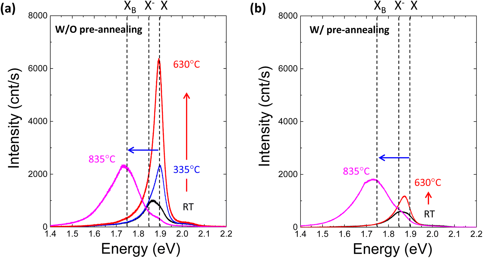 | ||
| Fig. 4 (a) Photoluminescence spectra for monolayer MoS2 annealed at different temperatures in the TDS chamber without preannealing in Ar. X, X− and XB represent exciton, trion and defect-induced bound exciton, respectively. The red arrow indicates the intensity enhancement with increasing annealing temperature from RT to 630 °C, while the blue arrow indicates the transition from exciton to defect-induced bound exciton due to high-temperature annealing at 835 °C. (b) Photoluminescence spectra for monolayer MoS2 annealed at different temperatures in the TDS chamber with preannealing in Ar. | ||
Four different types of experiments, namely, of TDS, AFM, Raman and PL, surprisingly, can be well explained by the two common kinds of defect formation mechanisms in the low and high annealing temperature regions. That is, at a low annealing temperature, the oxygen adsorbed on the basal plane of MoS2 flakes is the key factor, and it volatizes as SO2 by removing S from MoS2, leaving S vacancies. Then, at a high annealing temperature, direct S desorption becomes dominant. Here, it is reasonable to consider that defect formation at low annealing temperatures could be suppressed by removing oxygen adsorbed on MoS2 flakes before TDS annealing. To verify this idea, the MoS2 crystals were preannealed at 500 °C for one hour in an Ar gas flow to remove oxygen adsorbed on the MoS2 surface. Then, MoS2 flakes were transferred onto the SiO2/Si substrate by mechanical exfoliation in ambient air, followed by TDS annealing. The PL spectra of preannealed monolayer MoS2 are shown in Fig. 4b. The PL intensity enhancement at temperatures below 630 °C is greatly suppressed, which strongly indicates that S vacancy formation due to SO2 desorption was hindered due to the great reduction in oxygen adsorbed on the MoS2 surface. On the other hand, at a high temperature of 835 °C, the XB peak was almost the same, which is also evidence for direct S desorption. These results clearly support the two kinds of defect formation mechanisms in the low and high annealing temperature regions. To date, S vacancies have been experimentally observed and recognized as dominant defects because they have the lowest formation energy of ∼1.3–1.5 eV compared with other types of defects.3,4 However, this large formation energy could not explain the high S vacancy concentration of ∼1013 cm−2.50 The present study experimentally proves that oxygen adsorbed on MoS2 assists S vacancy formation by desorbing as SO2 since this O2-assisted S vacancy formation is energetically spontaneous at −0.49 eV.10
4. Conclusions
Through this experimental desorption study using TDS in combination with ALD, Raman, and PL, two kinds of S vacancy formation mechanisms are realized, that is, O2-assisted SO2 desorption at low annealing temperatures (400 °C to 650 °C) and direct S desorption at high annealing temperatures (over 800 °C). The key finding is that the initially adsorbed oxygen causes S vacancy formation through SO2 desorption. As a solution, the removal of oxygen is quite effective for preventing the formation of defects and further oxidation.Conflicts of interest
There are no conflicts to declare.Acknowledgements
This research was supported by the Mitsubishi Foundation, NEXCO Group Companies' support fund to Disaster Prevention Measures on Expressways, the JSPS A3 Foresight Program, JSPS KAKENHI (Grant Numbers: JP22H04957, JP21H05237, JP21H05233, and JP21H05232), NICT (Grant Number: 05901), and JST-Mirai Program (Grant Number: JPMJMI22708192), Japan.References
- S. B. Desai, S. R. Madhvapathy, A. B. Sachid, J. P. Llinas, Q. Wang, G. H. Ahn, G. Pitner, M. J. Kim, J. Bokor, C. Hu, H.-S. P. Wong and A. Javey, Science, 2016, 354, 99–102 CrossRef CAS PubMed.
- Y. Liu, X. Duan, H.-J. Shin, S. Park, Y. Huang and X. Duan, Nature, 2021, 591, 43–53 CrossRef CAS PubMed.
- J. Hong, Z. Hu, M. Probert, K. Li, D. Lv, X. Yang, L. Gu, N. Mao, Q. Feng, L. Xie, J. Zhang, D. Wu, Z. Zhang, C. Jin, W. Ji, X. Zhang, J. Yuan and Z. Zhang, Nat. Commun., 2015, 6, 6293 CrossRef CAS PubMed.
- W. Zhou, X. Zou, S. Najmaei, Z. Liu, Y. Shi, J. Kong, J. Lou, P. M. Ajayan, B. I. Yakobson and J.-C. Idrobo, Nano Lett., 2013, 13, 2615–2622 CrossRef CAS PubMed.
- S. McDonnell, R. Addou, C. Buie, R. M. Wallace and C. L. Hinkle, ACS Nano, 2014, 8, 2880–2888 CrossRef CAS PubMed.
- H. Qiu, T. Xu, Z. Wang, W. Ren, H. Nan, Z. Ni, Q. Chen, S. Yuan, F. Miao, F. Song, G. Long, Y. Shi, L. Sun, J. Wang and X. Wang, Nat. Commun., 2013, 4, 2642 CrossRef PubMed.
- N. Fang and K. Nagashio, J. Phys. D: Appl. Phys., 2018, 51, 65110 CrossRef.
- N. Fang, S. Toyoda, T. Taniguchi, K. Watanabe and K. Nagashio, Adv. Funct. Mater., 2019, 29, 1904465 CrossRef CAS.
- Z. Yu, Y. Pan, Y. Shen, Z. Wang, Z.-Y. Ong, T. Xu, R. Xin, L. Pan, B. Wang, L. Sun, J. Wang, G. Zhang, Y. W. Zhang, Y. Shi and X. Wang, Nat. Commun., 2014, 5, 5290 CrossRef CAS PubMed.
- J. Pető, T. Ollár, P. Vancsó, Z. I. Popov, G. Z. Magda, G. Dobrik, C. Hwang, P. B. Sorokin and L. Tapasztó, Nat. Chem., 2018, 10, 1246–1251 CrossRef PubMed.
- T. Yanase, F. Uehara, I. Naito, T. Nagahama and T. Shimada, ACS Appl. Nano Mater., 2020, 3, 10462–10469 CrossRef CAS.
- M. Makarova, Y. Okawa and M. Aono, J. Phys. Chem. C, 2012, 116, 22411–22416 CrossRef CAS.
- D. Rhodes, S. H. Chae, R. Ribeiro-Palau and J. Hone, Nat. Mater., 2019, 18, 541–549 CrossRef CAS PubMed.
- Q. Liang, Q. Zhang, X. Zhao, M. Liu and A. T. S. Wee, ACS Nano, 2021, 15, 2165–2181 CrossRef CAS PubMed.
- Y.-R. Chang, T. Nishimura and K. Nagashio, ACS Appl. Mater. Interfaces, 2021, 13, 43282–43289 CrossRef CAS PubMed.
- J. Gao, B. Li, J. Tan, P. Chow, T.-M. Lu and N. Koratkar, ACS Nano, 2016, 10, 2628–2635 CrossRef CAS PubMed.
- D. Lv, H. Wang, D. Zhu, J. Lin, G. Yin, F. Lin, Z. Zhang and C. Jin, Sci. Bull., 2017, 62, 846–851 CrossRef CAS.
- R. C. Longo, R. Addou, S. KC, J.-Y. Noh, C. M. Smyth, D. Barrera, C. Zhang, J. W. P. Hsu, R. M. Wallace and K. Cho, 2D Mater., 2017, 4, 025050 CrossRef.
- J. Martincová, M. Otyepka and P. Lazar, Chem.–Eur. J., 2017, 23, 13233–13239 CrossRef PubMed.
- Y. Li, Z. Zhou, S. Zhang and Z. Chen, J. Am. Chem. Soc., 2008, 130, 16739–16744 CrossRef CAS PubMed.
- M. Yamamoto, T. L. Einstein, M. S. Fuhrer and W. G. Cullen, J. Phys. Chem. C, 2013, 117, 25643–25649 CrossRef CAS.
- H. Zhu, X. Qin, L. Cheng, A. Azcatl, J. Kim and R. M. Wallace, ACS Appl. Mater. Interfaces, 2016, 8, 19119–19126 CrossRef CAS PubMed.
- J. Wu, H. Li, Z. Yin, H. Li, J. Liu, X. Cao, Q. Zhang and H. Zhang, Small, 2013, 9, 3314–3319 CAS.
- T. N. Walter, F. Kwok, H. Simchi, H. M. Aldosari and S. E. Mohney, J. Vac. Sci. Technol., B, 2017, 35, 21203 CrossRef.
- M. Liu, J. Shi, Y. Li, X. Zhou, D. Ma, Y. Qi, Y. Zhang and Z. Liu, Small, 2017, 13, 1602967 CrossRef PubMed.
- Q. Chen, H. Li, W. Xu, S. Wang, H. Sawada, C. S. Allen, A. I. Kirkland, J. C. Grossman and J. H. Warner, Nano Lett., 2017, 17, 5502–5507 CrossRef CAS PubMed.
- L. M. Farigliano, P. A. Paredes-Olivera and E. M. Patrito, J. Phys. Chem. C, 2020, 124, 13177–13186 CrossRef CAS.
- N. Ikegami, N. Ozawa, Y. Miyakawa, N. Hirashita and J. Kanamori, Jpn. J. Appl. Phys., 1992, 31, 2020–2024 CrossRef CAS.
- W. Widdra, S. I. Yi, R. Maboudian, G. A. D. Briggs and W. H. Weinberg, Phys. Rev. Lett., 1995, 74, 2074–2077 CrossRef CAS PubMed.
- S. K. Wang, K. Kita, C. H. Lee, T. Tabata, T. Nishimura, K. Nagashio and A. Toriumi, J. Appl. Phys., 2010, 108, 54104 CrossRef.
- Y.-R. Chang, N. Higashitarumizu, H. Kawamoto, F.-H. Chu, C.-J. Lee, T. Nishimura, R. Xiang, W.-H. Chang, S. Maruyama and K. Nagashio, Chem. Mater., 2021, 33, 186–194 CrossRef CAS.
- N. Takahashi, K. Watanabe, T. Taniguchi and K. Nagashio, Nanotechnology, 2015, 26, 175708 CrossRef CAS PubMed.
- Y. Xuan, Y. Q. Wu, T. Shen, M. Qi, M. A. Capano, J. A. Cooper and P. D. Ye, Appl. Phys. Lett., 2008, 92, 13101 CrossRef.
- H. G. Kim and H.-B.-R. Lee, Chem. Mater., 2017, 29, 3809–3826 CrossRef CAS.
- X. Wang, S. M. Tabakman and H. Dai, J. Am. Chem. Soc., 2008, 130, 8152–8153 CrossRef CAS PubMed.
- K. Ueno, J. Phys. Soc. Jpn., 2015, 84, 121015 CrossRef.
- K. Nagashio, T. Yamashita, T. Nishimura, K. Kita and A. Toriumi, J. Appl. Phys., 2011, 110, 24513 CrossRef.
- Y. Song, M. Park, J. Park, H. S. Ahn, T. K. Kim and S.-Y. Ju, Nanomaterials, 2022, 12 Search PubMed.
- D. E. Pierce, R. P. Burns, H. M. Dauplaise and L. J. Mizerka, Tribol. Trans., 1991, 34, 205–214 CrossRef CAS.
- C. Lee, H. Yan, L. E. Brus, T. F. Heinz, J. Hone and S. Ryu, ACS Nano, 2010, 4, 2695–2700 CrossRef CAS PubMed.
- L. Wang, X. Ji, F. Chen and Q. Zhang, J. Mater. Chem. C, 2017, 5, 11138–11143 RSC.
- K. F. Mak, C. Lee, J. Hone, J. Shan and T. F. Heinz, Phys. Rev. Lett., 2010, 105, 136805 CrossRef PubMed.
- H. Nan, Z. Wang, W. Wang, Z. Liang, Y. Lu, Q. Chen, D. He, P. Tan, F. Miao, X. Wang, J. Wang and Z. Ni, ACS Nano, 2014, 8, 5738–5745 CrossRef CAS PubMed.
- S. Mouri, Y. Miyauchi and K. Matsuda, Nano Lett., 2013, 13, 5944–5948 CrossRef CAS PubMed.
- D. Mastrippolito, S. Palleschi, G. D'Olimpio, A. Politano, M. Nardone, P. Benassi and L. Ottaviano, Nanoscale, 2020, 12, 18899–18907 RSC.
- S. Tongay, J. Suh, C. Ataca, W. Fan, A. Luce, J. S. Kang, J. Liu, C. Ko, R. Raghunathanan, J. Zhou, F. Ogletree, J. Li, J. C. Grossman and J. Wu, Sci. Rep., 2013, 3, 2657 CrossRef PubMed.
- E. Mitterreiter, B. Schuler, A. Micevic, D. Hernangómez-Pérez, K. Barthelmi, K. A. Cochrane, J. Kiemle, F. Sigger, J. Klein, E. Wong, E. S. Barnard, K. Watanabe, T. Taniguchi, M. Lorke, F. Jahnke, J. J. Finley, A. M. Schwartzberg, D. Y. Qiu, S. Refaely-Abramson, A. W. Holleitner, A. Weber-Bargioni and C. Kastl, Nat. Commun., 2021, 12, 3822 CrossRef CAS PubMed.
- K. Greben, S. Arora, M. G. Harats and K. I. Bolotin, Nano Lett., 2020, 20, 2544–2550 CrossRef CAS PubMed.
- N. Fang, K. Nagashio and A. Toriumi, 2D Mater., 2016, 4, 15035 CrossRef.
- Z. G. Yu, Y.-W. Zhang and B. I. Yakobson, Nano Lett., 2015, 15, 6855–6861 CrossRef CAS PubMed.
Footnote |
| † Electronic supplementary information (ESI) available. See DOI: https://doi.org/10.1039/d2na00636g |
| This journal is © The Royal Society of Chemistry 2023 |