
 Open Access Article
 This Open Access Article is licensed under a Creative Commons Attribution-Non Commercial 3.0 Unported Licence
Early stages of polycrystalline diamond deposition: laser reflectance at substrates with growing nanodiamonds†
David
Vázquez-Cortés
 ,
Stoffel D.
Janssens
,
Burhannudin
Sutisna
and
Eliot
Fried
*
,
Stoffel D.
Janssens
,
Burhannudin
Sutisna
and
Eliot
Fried
*
Mechanics and Materials Unit, Okinawa Institute of Science and Technology Graduate University, Okinawa 904-0495, Japan. E-mail: eliot.fried@oist.jp; Tel: +81-98-966-1372
First published on 1st December 2022
Abstract
The chemical vapor deposition of polycrystalline diamond (PCD) films is typically done on substrates seeded with diamond nanoparticles. Specular laser reflectance has been used in tandem with a continuous film model to monitor the thickness of these films during their deposition. However, approaches to gain information on properties that strongly affect film morphology, such as the areal density of seeds, remain largely unexplored. This work outlines a strategy for using laser reflectance measurements to refine the monitoring of film thickness during deposition, estimate the mean equivalent radii and the areal density of seeds, and estimate growth incubation periods. We present a general model based on the Rayleigh theory of scattering for laser reflectance at substrates with growing nanoparticles that captures the early stages of PCD deposition. We test our model experimentally by depositing diamond under identical conditions on silicon substrates with various seed densities and by comparing seed densities obtained by scanning electron microscopy to those determined by our strategy. We also explore the different deposition stages for which our model and a continuous film model can be used safely. In addition to providing guidelines for characterizing PCD deposition, this work may also advance the general understanding of nanoparticle growth and formation.
1 Introduction
1.1 Motivation and goals
According to Russell,1 the term “incubation time”, which is used interchangeably with “incubation period”,2 “induction time”,3 and “induction period”,4 describes thermally activated processes that do not commence immediately after establishing a reaction temperature. A prime example of a thermally activated process is the chemical vapor deposition (CVD) of polycrystalline diamond (PCD).5 Due to high activation energies associated with the nucleation of diamond grains on foreign substrates, relative to those of diamond deposition, incubation periods preceding deposition are observed.6–8 Such incubation periods can be reduced significantly, or even eliminated entirely, by seeding diamond nanoparticles, typically detonation nanodiamonds, on substrates before deposition.9 Still, the seeding step does not prevent incubation under certain deposition conditions.8,10,11 Incubation can be related to the etching of seeds,2 which affects the seed density. Consequently, the morphological features of films and the physical properties such as thermal conductivity, transparency, and adhesiveness are also affected.12–14 Incubation is mainly inferred from laser reflectance measurements. However, approaches to systematically obtain incubation periods and to gain information on properties that strongly affect film morphology, such as the areal density of seeds, from these measurements remain largely unexplored.This work outlines a strategy for using laser reflectance measurements to estimate incubation periods, estimate the mean equivalent radii and the areal density of seeds, and refine the monitoring of film thickness during deposition. The specific goals of this work are to:
• Develop a semiquantitative, non-interference, and non-continuous film model for specular laser reflectance based on nanodiamond particle scattering that captures the early stages of PCD CVD on seeded substrates.
• Test our model experimentally by depositing diamond on substrates with different seed densities and by analyzing the samples with several microscopy techniques.
• Explore the different deposition stages for which our model and a continuous film model can be used safely.
• Develop a method to estimate incubation periods, which we identify with a delay in deposition and/or a reduced deposition rate during the early stages of deposition, with specular laser reflectance.
For brevity, “specular laser reflectance” is shortened to “laser reflectance”. The term “diamond particle” refers to a single grain or to a cluster of grains isolated from other diamond particles and the term “seed” refers to a diamond particle deposited on the surface of a substrate before deposition.
1.2 Background
The small lattice parameter and the high surface energies of diamond limit diamond heteroepitaxy to diamond-on-iridium.15–20 An alternative method to deposit diamond on foreign substrates relies on seeding the substrate surface with diamond particles.21–28 Most work on seeding aims to increase the areal (seed) density with the objective of minimizing the thickness at which films become pinhole-free.29–31 However, high seed densities are not always desirable. For example, Mandal et al.32 found that a low seed density reduces stress in a PCD film grown on an aluminum nitride substrate, affording the deposition of a thicker film without delamination. Tsigkourakos et al.33 found that lowering the seed density increases the electrical conductance of boron-doped films by one order of magnitude, and Janssens et al.34 showed, through simulations, that the seed density strongly affects the grain size distribution. These results show that the seed density is a useful parameter for tuning the properties of PCD films and is therefore explored systematically in this work.In situ laser reflectance interferometry is widely used for monitoring the thickness of a nanocrystalline diamond film during deposition. This is done by shining a laser beam on a sample, collecting the specularly reflected light with a photodetector, and analyzing the output signal that the photodetector produces.35–37Fig. 1 shows a schematic of a reflectance setup installed on a CVD reactor. The film thickness and deposition rate are typically calculated from the extrema of the oscillating reflectance and the time intervals separating these extrema, respectively.4,38,39 The oscillations are caused by thin film interference.
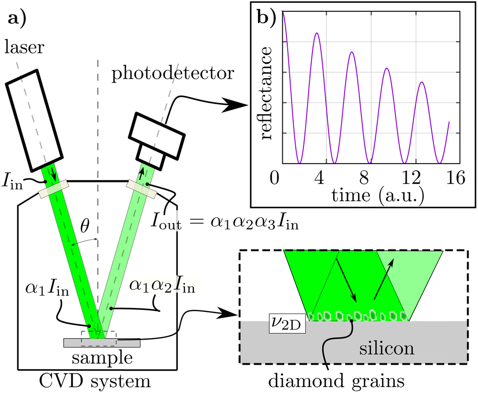 | ||
| Fig. 1 Schematic of a reflectance setup. (a) Schematic of a setup for measuring the specular laser reflectance of a sample in a chemical vapor deposition (CVD) system during deposition. A laser beam of intensity Iin enters the CVD system at an angle θ. After interaction with the windows and the sample, the beam exits the system with intensity Iout. The arrows indicate the propagation direction of the laser beam. The windows cause attenuations α1 and α3, and attenuation α2 is caused by the sample. The detailed view of the dashed rectange in (a) shows a schematic of diamond particles at the outset of deposition, with seed density ν2D. (b) A typical graph obtained by plotting the photodetector's signal in (a) as a function of time. Regular oscillations, which are used for deposition rate estimation, are observed for thin-film interference. | ||
In the early stage of diamond deposition on seeded silicon substrates, laser reflectance decays more slowly than expected for a continuous film.18,39 Some authors have related the initial slow decay of the reflectance to a reduced deposition rate or to the varying roughness of the sample surface.2,38 For the deposition of diamond on seeded substrates, the existence of incubation is mainly derived from the slow decay in reflectance during the early stages of deposition. However, it is not clear whether the estimation of an incubation period is strongly affected by the assumption of a continuous film. Here, we investigate this systematically by comparing laser reflectance with atomic force microscopy (AFM) and scanning electron microscopy (SEM).
Bonnot et al.40 showed that during the early stages of PCD deposition, scattering from isolated diamond seeds increases with time. This increase was measured by installing a detector away from the specularly reflected laser. The analysis of the measured scattering was done using a model based on Rayleigh scattering, assuming that scattering caused by seeds is proportional to the square of their volume. This made it possible to calculate the diamond deposition rate using scattering instead of reflectance. As demonstrated by Smolin et al.,41 Mie scattering, which generalizes Rayleigh scattering to large particles, can also explain the reflectance behavior during the initial stage of deposition. Smolin et al. measured reflectance by introducing a laser beam through a quartz window directed normal to the substrate surface and by measuring the specularly reflected beam intensity with a photodiode. However, the experiments reported in their work were limited by the control over seeding available at the time. Also, the implications of varying the diamond seed density on reflectance were not systematically investigated. These works demonstrate that light scattering, rather than interference, can accurately describe light-sample interactions during the early stages of PCD deposition. However, to the best of our knowledge, a relation that describes the reflectance during the early stages of PCD deposition has not yet appeared in the literature. Moreover, we are not aware of any previous attempt to include light scattering phenomena in the analysis of reflectance curves measured during incubation. We, therefore, develop an elementary model based on the Rayleigh theory of scattering to explain the behavior of laser reflectance during the early stages of PCD deposition and test the model experimentally.
Due to the non-interference nature of the light–sample interaction in the early stages of PCD deposition, we avoid using the term “laser reflectance interferometry” and opt for the more general term “laser reflectance”.
2 Model
2.1 Laser beam–sample interaction
A standard reflectance setup mounted on a CVD system is shown in Fig. 1. From linear optics, the attenuation α of a beam with intensity Iin entering the CVD system during diamond deposition is given by | (1) |
| α = α1α2α3, | (2) |
| α2 = α21α22. | (3) |
 | (4) |
The voltage measured by the photodetector, as depicted in Fig. 1a, is proportional to the responsivity r of the detector. Dividing the voltage V measured in the presence of diamond particles by the voltage V0 measured for a bare silicon substrate, we obtain the relative voltage
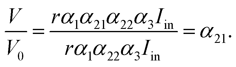 | (5) |
2.2 Scattering caused by a collection of particles constrained in a plane
To obtain a relation for α21, we first recognize that the intensity change, per unit length, dI/dz of a beam with initial intensity I0 traveling in a non-absorbing host fluid containing particles with number density per unit volume ν can be expressed as | (6) |
 | (7) |
| ΔI = −I0ν2DσR, | (8) |
| I = I0 + ΔI = I0(1 − ν2DσR). | (9) |
 | ||
| Fig. 2 Model for calculating scattering caused by growing diamond particles. (a) Schematic of an imaginary experimental setup to calculate the scattering caused by a collection of uniform size diamond particles constrained to a plane. The beam exits the laser with intensity I0, and the intensity after interaction with the particles is reduced to I. The particles are assumed to be spherical and of the same radius a. (b) To obtain a experimentally, we measure the projected area A of a diamond particle, calculate the radius r of the circle with area A′ for which A = A′, and take the mean value of r for all the particles. (c) Uniform deposition on an equivalent seed with radius a0 at the outset of the deposition is depicted. The radius of the particle is the sum of a0 and the deposited thickness d. The deposited thickness is expressed as d = vdt, with vd and t denoting deposition rate and deposition time, respectively. | ||
A beam with oblique incidence at angle θ interacts with an effective density of particles given by ν2D/cos![[thin space (1/6-em)]](https://www.rsc.org/images/entities/char_2009.gif) θ. Replacing ν2D in (9) with ν2D/cosθ and dividing by I0, we observe that the attenuation of this beam after interaction with a collection of particles constrained on a plane can be expressed as
θ. Replacing ν2D in (9) with ν2D/cosθ and dividing by I0, we observe that the attenuation of this beam after interaction with a collection of particles constrained on a plane can be expressed as
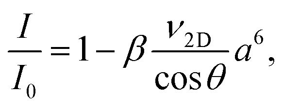 | (10) |

Relation (10) is valid for a collection of isolated, relatively small, and uniformly sized spherical particles. However, in processes of interest here, seeds are randomly positioned on the silicon substrate after seeding, and their size is not uniform. Also, diamond particles grow homoepitaxially from the seeds and coalesce during deposition, which affects ν2D. Without performing a complete statistical analysis of the growth and coalescence of diamond particles, we model the relative reflectance R in the initial stages of diamond deposition using α21 = I/I0 and assuming that:
• The diamond particles are sufficiently small to ensure that the Rayleigh approximation applies.
• Particle clustering, which reduces particle density, can be ignored.
• Diamond particles can be represented by uniformly sized spheres of radius a. The method for obtaining a experimentally is described in Fig. 2b and its caption.
• The particle size increases uniformly. Consequently, the radius a increases as
| a = a0 + d, | (11) |
| d = vdt, | (12) |
With these provisions, the length a in (10) represents the mean equivalent radius of a collection of diamond particles. Using (10) in (4), we obtain
 | (13) |
| a = a0 + vdt. | (14) |
 | (15) |
3 Experiment
Diamond deposition was performed on 2 × 2 cm silicon substrates cleaved from 100 mm diameter phosphorus-doped silicon wafers with a resistivity of 1–10 Ω cm obtained from Electronics and Materials Corporation, Limited. After cleaving, the substrates were cleaned by a sequential ultrasonic bath in deionized (DI) water, acetone, isopropanol, and DI water for 5 min each. The substrates were then immersed for 10 min in Semicoclean solution obtained from Furuuchi Chemical Corporation, rinsed in DI water, and dried with high purity nitrogen. After the cleaning process, the substrates were exposed to an air plasma in a PR200 Plasma reactor obtained from Yamato Scientific Corporation, Limited to improve the wettability of their surfaces. The plasma power and exposure time were set to 170 W and 60 s, respectively, and the airflow rate was kept at 100 sccm. Immediately after the plasma treatment, the substrates were transferred to a spin coater, where they were seeded with suspensions of various nanodiamond concentrations. Cleaning and seeding were done without pause to avoid airborne surface contamination affecting the seeding.43 The seeding procedure was done by drop casting 150 μL of nanodiamond suspension on an immobile substrate. One minute after drop casting the suspension, the sample was spun at a rotation speed of 6000 rpm for 30 s while flushing the wetted surface with DI water for the first 5 s of spinning.Nanodiamond suspensions were made by dispersion of NanoAmando Hard Hydrogel detonated nanodiamond powder obtained from NanoCarbon Research Institute Corporation, Limited in 0.2 L of DI water at a proportion of 0.5 g L−1, and ultrasonication of the mixture with an Epishear probe sonicator with tip diameter 3.2 mm and length 4.5 cm. This was achieved using an ultrasonic transducer with a power of 100 W and a frequency of 20 kHz. To avoid overheating the system, an on/off cycle of 1 s/1 s was fixed for 90 min. The obtained suspension was centrifuged at 15000 rpm for 30 min to remove large agglomerates of more than 140 nm. The supernatant was recovered and diluted with DI water to obtain concentrations of 10–60% with respect to the as-centrifuged supernatant concentration of 100%.
Diamond was deposited on the seeded substrates using an SDS6500X microwave plasma-assisted CVD system from Cornes Technologies. For all samples, PCD was deposited with a plasma power of 1500 W, a hydrogen flow rate of 288 sccm, a methane flow rate of 12 sccm, and a chamber pressure of 15 torr. This was done using programmed recipes to ensure repeatability. The microwaves and the plasma in the CVD chamber heated the substrate. The temperature of each sample was found to stabilize at 530 ± 8 °C, as measured by an FLHX-PNE0300 infrared thermometer with a spectral range of 0.6–1.8 μm from Japan Sensor Corporation with emissivity set to 0.6. The deposition was monitored in situ by a homemade laser reflectance setup consisting of a 1 mW power semiconductor laser emitting at 532 nm that was directed to the sample through a viewport in the CVD chamber at angle θ equal to approximately 20°. A schematic of this setup is provided in Fig. 1a. A silicon photodetector collected the reflected light from the substrate surface. A laser line filter centered at 532 nm with an FWHM of 1 nm was positioned between the viewport and the silicon photodetector to avoid plasma emission from reaching the photodetector.
The measured deposition rate was 0.6 ± 0.05 nm min−1 obtained by growing a reference sample for 5 h. The thickness of the calibration layer was 180 nm, as measured with an optical nanogauge C13027-11 obtained from Hamamatsu Photonics and corroborated by cross-section scanning electron microscopy (SEM) observation. Seeded substrates were characterized using a JEOL JSM-7900F scanning electron microscope obtained from JEOL. Analysis of the SEM images was automated by a Python (https://www.python.org) script that makes use of the Image-J (https://imagej.net/Fiji) bandpass filter to denoise the original images and the OpenCV “findContours()” function for the particle analysis. The number density ν2D is the number of isolated particles recognized by the Python script and averaged over five images at 50000× magnification from different portions on the substrates. After the deposition, the samples were characterized by atomic force microscopy (AFM) on an Agilent 5500 scanning probe microscope obtained from Keysight Technologies using silicon probes with 7 nm nominal radius, 14 μm nominal cantilever length, a nominal cantilever resonance frequency of 300 kHz and a 26 N m−1 spring constant. AFM image analysis and profile extraction were done using Gwyddion (https://gwyddion.net). Statistical analysis of particle size was done by particle marking using the “watershed” method.44
4 Results and discussion
4.1 Predictions of the model
To understand the implications of our model, we plot the relative reflectance R versus t using the Rayleigh scattering relation (15) for various choices of vd with a0 = 20 nm and ν2D = 1 × 1010 cm−2. Fig. 3a shows that R decays more slowly as vg decreases. To avoid confusing this effect with the presence of incubation, we use (12) and (15) to express R in terms of d: | (16) |
 | ||
| Fig. 3 Simulated reflectance during diamond deposition. (a) Relative reflectance R calculated using (15) for diamond deposition on seeded substrates as a function of deposition time t for various deposition rates. (b) R calculated using (16) as a function of deposited thickness d for various values of ν2D. Radius a0 was set to 20 nm for all calculations. The black curve in (b) corresponds to the normalized reflectance for a continuous diamond film calculated by the transfer-matrix method.45 | ||
In a review on nanocrystalline diamond by Williams,2R is plotted as a function of t for diamond deposition on seeded substrates. The reflectance curves exhibit a decay that reduces as the methane concentration in the gas phase reduces. This trend is reasoned to be caused by an extension of the incubation period as the methane concentration is reduced. However, by assuming that vd is proportional to the methane concentration, a possible alternative explanation is that a reduced methane concentration produces a lower deposition rate that delays the reflectance decay. The reality is probably a combination of both descriptions since a plasma with lower methane concentration might etch grains, leading to incubation. To resolve the ambiguity regarding the existence of incubation, we refer to a method delineated in our previous work8 for estimating incubation periods. In Section 4.3, we extend this method.
4.2 Experimental verification of the model
We test our model by comparing the relative reflectance R during diamond deposition on seeded substrates with various values of ν2D. The values of ν2D and a0 were obtained by SEM analysis. The Rayleigh scattering relation (15) was fitted to the reflectance curves obtained during diamond deposition using the parameters ν2D, a0, and V0. The values of ν2D and a0 were compared with those obtained from SEM. After deposition, the surface morphology of the samples was analyzed by AFM. Finally, the height distributions of diamond particles were correlated to the reflectance measurements. | ||
| Fig. 4 Seed density. (a) SEM image of a sample seeded using a suspension of concentration x = 10%. (b) SEM image of a sample seeded with an x = 100% suspension. (c) Seed density ν2D and surface coverage as function of x. Density ν2D is defined as the number of isolated diamond particles in the image, divided by the total area. For the linear regression the value of ν2D for x = 100% is not considered. | ||
In the work of Tsigkourakos et al.33 the surface coverage was found to vary non-linearly for suspension concentrations in the range of 0.002 g L−1 to 2 g L−1. Recognizing that nanodiamonds in suspension tend to aggregate relatively fast at low concentrations,46 we hypothesize that nanodiamond agglomerates were seeded in that work. Scorsone et al.29 obtained good linearity between ν2D and nanodiamond concentration in the suspension. Still, the suspension preparation required the addition of polyvinyl alcohol and ultrasonication at 40 °C for 2 h. In the work described here, we simply diluted a stock suspension immediately before seeding to avoid dilution-induced agglomeration.
 | ||
| Fig. 5 Experimental and simulated reflectance curves. Laser reflectance R as a function of the deposition time t and the deposited thickness d. R is monitored during the deposition of diamond on silicon substrates seeded with nanodiamond suspension of concentrations ranging from 10% to 100% relative to the stock suspension. The dashed black curves correspond to fitting (15) to the experimental curves. The green and dark yellow vertical dashed lines indicate the start and end of the deposition, respectively. The blue dashed line indicates the time at which the plasma is ignited. | ||
As predicted by our model, the decay of R as a function of d is inversely proportional to ν2D. In contrast to findings reported in the existing literature, our measurements show that a diminished decay of R is not per se related to incubation. Evidence for incubation is mainly based on literature2,4 that describes polycrystalline diamond deposition by the bias-enhanced nucleation method. Stoner4 found that in the initial stage of diamond deposition, by this method, incubation is observed, during which no diamond deposition occurs. This has been corroborated by Jiang et al.3 using AFM measurements which showed that diamond nuclei were not created until after 6.5 min of plasma exposure. In the works of Stoner and Jiang et al., incubation is ascribed to diamond nucleation that starts after the silicon substrate is saturated with carbon. For polycrystalline diamond deposition on seeded substrates under harsh conditions, we previously showed that incubation is present due to seed etching.8 However, under mild conditions similar to those used in this work, incubation has never been corroborated (to the best of our knowledge).47,48
Quantitative results are obtained by non-linear least-square fitting of (15) with the values vd = 0.6 nm min−1, np = 2.41, ng = 1, and λ0 = 532 nm and fitting parameters ν2D, a0, and V0. The fitting ranges are manually adjusted and are listed in Table 1. From the dashed curves in Fig. 5, we observe that the fits for samples seeded using low-concentration diamond suspensions are good over the entire deposition interval. However, the fits and the experimental data diverge for high concentrations before the deposition ends. This can be attributed to the proximity of neighboring particles for samples with high seed densities. When the radius of a diamond particle exceeds half of the distance to its nearest neighbor, they coalesce and form a larger particle. This phenomenon has two consequences:
| Sample% | ν 2D (SEM) × 109 cm−2 | a 0 (SEM) nm | ν 2D (fitting) × 109 cm−2 | a 0 (fitting) nm | Fitting range d nm |
|---|---|---|---|---|---|
| 10 | 1.9 | 19 | 0.9 | 10 | 10–69 |
| 20 | 3.4 | 20 | 1.6 | 13 | 10–67 |
| 30 | 5.2 | 22 | 1.8 | 14 | 10–65 |
| 40 | 6.8 | 21 | 2.8 | 14 | 10–63 |
| 50 | 10.2 | 21 | 3.9 | 14 | 10–61 |
| 60 | 11.3 | 22 | 5.5 | 18 | 10–41 |
| 100 | 10.1 | 27 | 8.4 | 23 | 10–29 |
(1) The diamond particle density ν2D will be reduced due to coalescence.
(2) Coalesced particles may be larger than the wavelength for which the Rayleigh scattering approximation holds, leading to significant discrepancies between the model and the experimental data.
Once all diamond particles coalesce to form a continuous layer of polycrystalline diamond, which we called the closed-film threshold in our previous work,34 the reflectance signal can be described using the transfer matrix method.45 By visual inspection, it is also evident that the fitting curves coincide with experimental data up to a reflectance value of 0.7 ± 0.1, which we interpret as the empirical reflectance limit above which our model can be applied with confidence.
Values for ν2D obtained by fitting the curves in Fig. 5 are shown in Table 1 and values for ν2D estimated by SEM analysis in Section 4.2.1 are also shown for comparison. Fig. 6 shows that except for the sample grown on the substrate seeded with the 100% concentration suspension, the values for ν2D obtained by SEM analysis are proportional to those obtained by fitting using the Rayleigh scattering relation (15) with a proportionality constant of 0.44.
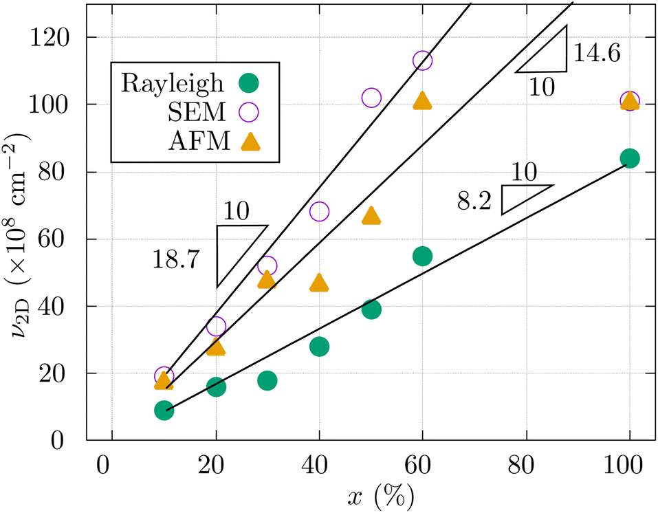 | ||
| Fig. 6 Estimated diamond particle densities. Diamond particle density ν2D, as a function of the concentration x, obtained by (i) fitting the Rayleigh scattering relation (15) to the reflectance curves displayed in Fig. 5, (ii) the SEM image analysis that is delineated in Section 4.2.1 (before deposition), and (iii) AFM particle marking that is delineated in Section 4.2.3 (after deposition). For the linear regression, the values of ν2D at 100% obtained by SEM and AFM are not considered. | ||
Fig. 7a contains examples of AFM images before and after particle marking. A complete set of images can be found in Fig. S2 of the ESI.† The particle height distributions are shown in Fig. 7b, and the maximum and minimum height as a function of x are provided in Fig. 7c. From this data, we find that (i) the particle height at the maximum frequency increases as x increases, (ii) the maximum height (114 ± 10 nm) is not significantly dependent on x, and (iii) the minimum height increases as x increases. These findings can be explained as follows. During deposition, smaller particles are buried by larger particles.50 Burying occurs more frequently as ν2D increases because the mean distance between particles decreases as ν2D increases. Consequently, the particle height at the maximum frequency and the minimum particle height shift towards larger values. In this scenario, the particle of maximum height is not affected by burying and its height is independent of ν2D provided that vd is constant for all the samples, as we assume to be so.
 | ||
| Fig. 7 AFM particle analysis. (a) AFM images of samples seeded with suspensions of concentration x = 10% and x = 100%, before and after applying the watershed method for marking particles. (b) Height distribution and (c) the maximum and the minimum height of particles found in the analysis of two AFM images of each sample. | ||
4.3 Seed density versus mean film thickness
Since surface roughness decreases after film closure38 and the maximum grain height is independent of ν2D, as shown in Section 4.2.3, the mean film thickness should become less dependent on ν2D as the deposited thickness increases. As a consequence, we hypothesize that the R curves for samples grown on a substrate with dissimilar ν2D should show extrema at values of d that become more similar as d increases. Using Fig. 8a, we test this hypothesis by comparing R as a function of d for samples SL and SH with ν2D = 1.00 × 1010 cm−2 and ν2D = 2.95 × 1010 cm−2, respectively, as measured by SEM. While the R curve for SL exhibits the first minimum at approximately d = 86.0 nm, the first minimum for the R curve of SH is at approximately d = 61.5 nm. On the other hand, the position of the second minimum is about d = 178 nm and d = 168 nm for SL and SH, respectively. The difference in d for the second minimum is only 10 nm, which is considerably smaller than the 24.5 nm observed for the first minimum and, therefore, supports our hypothesis. | ||
| Fig. 8 Film deposition after the early stages of deposition. (a) Reflectance data measured during diamond deposition plotted versus deposited thickness d of samples SL and SH with seed density ν2D equal to 1.00 × 1010 cm−2 and 2.95 × 1010 cm−2, respectively. The plots show that after depositing 180 nm of diamond, the positions of the minima tend to the same value of d. (b) and (c) Show SEM cross-sections of SL and SH, respectively. Both images show that SL and SH have similar thicknesses (180 nm), but the RMS surface roughness of SL appears larger than that of SH. A red dashed line in (b) or (c) indicates the substrate–diamond interface. | ||
Fig. 8b and c show the SEM cross-section of SL and SH, respectively. From these cross-sections, we deduce that the mean film thickness is similar in both samples, which is in line with SL thickness 182 nm and SH thickness 184 nm that we obtained by an optical nanogauge. From these cross sections, we also observe that the surface of SL is rougher than that of SH. We verify and quantify this by analyzing AFM data, obtained from two 5 × 5 μm2 areas measured at different positions, for each sample. AFM images from these samples and their profiles along the selected lines are shown in Fig. S3 of the ESI.† The result of the analysis is 14.6 nm and 11.0 nm RMS surface roughness for SL and SH, respectively. This difference in surface roughness might contribute to the difference in d for the second minima in Fig. 8a. In addition to surface roughness, we hypothesize that voids at the substrate–film interface might also contribute to this difference.
The results presented in the present section also show that even for a relatively low value of ν2D, the continuous film model can provide a reasonable approximation of the mean film thickness beyond the early stages of deposition.
4.4 Estimation of incubation periods by laser reflectance
To systematically obtain an incubation period and the deposition rate by laser reflectance, we use the findings presented in this work to extend a previously proposed method.8 To quantify the incubation period, we collect the values of t where the extrema in R occur. A schematic of such a curve is provided in Fig. 9a. Subsequently, we estimate the incremental thickness h = lΔh, which we define as the thickness at the lth extremum, calculated for a continuous film. The thickness Δh is a constant that can be calculated with the relations | (17) |
 | ||
| Fig. 9 Schematic reflectance to depict the method to estimate the incubation period. (a) Typical reflectance R curve obtained during diamond deposition on seeded substrates as a function of time t where extrema are numbered. (b) Incremental thickness h as a function of t for the curve in (a). The values of h are calculated with (17). | ||
In the event that few or no extrema are observed, more sophisticated characterization techniques such as “specific zone marking”,36 that enable the observation and measurement of localized diamond particles before and after diamond deposition, can be used.
5 Conclusions
The chemical vapor deposition of polycrystalline diamond (PCD) films is typically done on substrates seeded with diamond nanoparticles. In this work, we outlined a strategy for using laser reflectance measurements to refine the monitoring of film thickness during deposition, estimate the mean equivalent radii and the areal density of seeds, and estimate growth incubation periods. We presented a simple model to describe specular laser reflectance in the early stages of PCD deposition. The reflectance behavior predicted by our model differed from that of a continuous film, which is well-described by a continuous film model, and this difference enlarged as the seed density used in our model decreased. These predictions were tested and confirmed by in situ specular laser reflectance measurements of diamond deposition on silicon substrates with various seed densities. A relation for reflectance found in our model was fitted to the experimental reflectance data, and the seed density obtained by fitting was found to be proportional to the seed density obtained by scanning electron microscopy analysis. Post-deposition atomic force microscopy data analysis showed that the deposition rate is independent of the seed density, which supports an assumption made in our model. Other deposition experiments showed that the continuous film model can be used safely beyond the early stages of deposition. We also showed that relying on the continuous film model for describing the early stages of deposition can result in questionable conclusions regarding the presence of incubation or the duration of incubation periods. Inspired by this, we proposed a method for estimating incubation periods together with a deposition rate, based on laser reflectance measurements. Our work provides guidelines for using laser reflectance as a tool to elucidate and guide the deposition of PCD films with tailored properties. Our work may also advance the general understanding of nanoparticle growth and formation.Conflicts of interest
There are no conflicts to declare.Nomenclature
| a | Mean equivalent radius |
| a 0 | Mean equivalent radius of diamond seeds |
| α | Total beam attenuation caused by the CVD system |
| α 1 | Beam attenuation caused by entering the CVD system |
| α 2 | Beam attenuation caused by the sample |
| α 21 | Beam attenuation caused by the diamond particles on the silicon substrate |
| α 22 | Beam attenuation caused by the total reflectance of the silicon substrate |
| α 3 | Beam attenuation caused by exiting the CVD system |
| β |

|
| d | Deposited thickness |
| σ | Scattering cross section |
| σ R | Rayleigh scattering cross section |
| I 0 | Beam intensity before interaction with small particles |
| I | Beam intensity |
| I in | Beam intensity entering the CVD system |
| I out | Beam intensity leaving the CVD system |
| l | Sequence number of an extremum |
| λ 0 | Beam wavelength in the medium |
| m | Ratio np/ng |
| n g | Refractive index of the medium |
| n p | Refractive index of the particles |
| ν | Number density per unit volume |
| ν 2D | Nanodiamond seed density |
| R | Relative reflectance |
| r | Equivalent radius |
| t | Time |
| θ | Angle of incidence |
| V | Voltage measured during diamond deposition |
| V 0 | Voltage for a beam reflected on a bare silicon substrate |
| v d | Deposition rate |
| x | Suspension concentration |
Acknowledgements
The authors thank the Okinawa Institute of Science and Technology Graduate University (OIST) for the financial support, with subsidy funding from the Cabinet Office, Government of Japan. The authors also thank T. Sasaki, from the Scientific Imaging Section at OIST, for the assistance and technical guidance on SEM measurements. S. D. J. and E. F. acknowledge JSPS KAKENHI funding grant number JP21K03782, and B. S. acknowledge JSPS KAKENHI (Grants-in-Aid for Early-Career Scientists) grant number JP20K15347.References
- K. C. Russell, Grain boundary nucleation kinetics, Acta Metall., 1969, 17, 1123–1131 CrossRef CAS
.
- O. A. Williams, Nanocrystalline diamond, Diamond Relat. Mater., 2011, 20(5), 621–640 CrossRef CAS
- X. Jiang, K. Schiffmann and C.-P. Klages, Nucleation and initial growth phase of diamond thin films on (100) silicon, Phys. Rev. B: Condens. Matter Mater. Phys., 1994, 50, 8402–8410 CrossRef CAS PubMed
- B. R. Stoner, B. E. Williams, S. D. Wolter, K. Nishimura and J. T. Glass, In situ growth rate measurement and nucleation enhancement for microwave plasma CVD of diamond, J. Mater. Res., 1992, 7(2), 257–260 CrossRef CAS
- J. E. Butler and A. V. Sumant, The CVD of nanodiamond materials, Chem. Vap. Deposition, 2008, 14(7–8), 145–160 CrossRef CAS
- K. A. Snail and C. M. Marks, In situ diamond growth rate measurement using emission interferometry, Appl. Phys. Lett., 1992, 60(25), 3135–3137 CrossRef CAS
- A. Yamaguchi, M. Ihara and H. Komiyama, Temperature dependence of growth rate for diamonds grown using a hot filament assisted chemical vapor deposition method at low substrate temperatures, Appl. Phys. Lett., 1994, 64(10), 1306–1308 CrossRef CAS
- A. Giussani, S. D. Janssens, D. Vázquez-Cortés and E. Fried, Evolution of nanodiamond seeds during the chemical vapor deposition of diamond on silicon substrates in oxygen-rich plasmas, Appl. Surf. Sci., 2022, 581, 152103 CrossRef CAS
- S. Iijima, Y. Aikawa and K. Baba, Early formation of chemical vapor deposition diamond films, Appl. Phys. Lett., 1990, 57(25), 2646–2648 CrossRef CAS
- S. Stehlik, M. Varga, P. Stenclova, L. Ondic, M. Ledinsky, J. Pangrac, O. Vanek, J. Lipov, A. Kromka and B. Rezek, Ultrathin nanocrystalline diamond films with silicon vacancy color centers via seeding by 2 nm detonation nanodiamonds, ACS Appl. Mater. Interfaces, 2017, 9(44), 38842–38853 CrossRef CAS PubMed
- A. Kromka, Š. Potocký, J. Čermák, B. Rezek, J. Potměšil, J. Zemek and M. Vaněček, Early stage of diamond growth at low temperature, Diamond Relat. Mater., 2008, 17(7), 1252–1255 CrossRef CAS
- Y.-C. Lee, S.-J. Lin, C.-Y. Lin, M.-C. Yip, W. Fang and I.-N. Lin, Pre-nucleation techniques for enhancing nucleation density and adhesion of low temperature deposited ultra-nanocrystalline diamond, Diamond Relat. Mater., 2006, 15(11), 2046–2050 CrossRef CAS
- J. Anaya, T. Bai, Y. Wang, C. Li, M. Goorsky, T. L. Bougher, L. Yates, Z. Cheng, S. Graham, K. D. Hobart, T. I. Feygelson, M. J. Tadjer, T. J. Anderson, B. B. Pate and M. Kuball, Simultaneous determination of the lattice thermal conductivity and grain/grain thermal resistance in polycrystalline diamond, Acta Mater., 2017, 139, 215–225 CrossRef CAS
- L. Huang, T. Wang, X. Li, X. Wang, W. Zhang, Y. Yang and Y. Tang, UV-to-IR highly transparent ultrathin diamond nanofilms with intriguing performances: Anti-fogging, self-cleaning and self-lubricating, Appl. Surf. Sci., 2020, 527, 146733 CrossRef CAS
- J. Millán-Barba, M. Gutiérrez, F. Lloret, R. G. de Villoria, R. Alcántara, K. Haenen and D. Araujo, Study of early stages in the growth of boron-doped diamond on carbon fibers, Phys. Status Solidi A, 2021, 218(5), 2000284 CrossRef
- S. S. Nicley, S. Drijkoningen, P. Pobedinskas, J. Raymakers, W. Maes and K. Haenen, Growth of boron-doped diamond films on gold-coated substrates with and without gold nanoparticle formation, Cryst. Growth Des., 2019, 19(6), 3567–3575 CrossRef CAS
- J. Delchevalrie, S. Saada, R. Bachelet, G. Saint-Girons and J. C. Arnault, Spectroscopic ellipsometry: A sensitive tool to monitor domains formation during the bias enhanced nucleation of heteroepitaxial diamond, Diamond Relat. Mater., 2021, 112, 108246 CrossRef CAS
- G. Cicala, V. Magaletti, G. S. Senesi and M. Tamborra, Smoothness improvement of micrometer- and submicrometer-thick nanocrystalline diamond films produced by MWPECVD, J. Nanopart. Res., 2013, 15(4), 1549 CrossRef
- M. Schreck, J. Asmussen, S. Shikata, J. C. Arnault and N. Fujimori, Large-area high-quality single crystal diamond, MRS Bull., 2014, 39, 504–510 CrossRef CAS
- S.-W. Kim, Y. Kawamata, R. Takaya, K. Koyama and M. Kasu, Growth of high-quality one-inch free-standing heteroepitaxial (001) diamond on (11 2 0) sapphire substrate, Appl. Phys. Lett., 2020, 117(20), 202102 CrossRef CAS
- R. C. M. de Barros, E. J. Corat, N. G. Fereira, T. M. de Souza, V. J. Trava-Airoldi, N. F. Leite and K. Iha, Dispersion liquid properties for efficient seeding in CVD diamond nucleation enhancement, Diamond Relat. Mater., 1996, 5(11), 1323–1332 CrossRef
- C. Norgard, K. Glejbol, S. S. Eskildsen and A. Matthews, Enhanced diamond nucleation density utilising seeding, Diamond Relat. Mater., 1998, 7, 1278–1281 CrossRef CAS
- R. Akhvlediani, I. Lior, S. Michaelson and A. Hoffman, Nanometer rough, sub-micrometer-thick and continuous diamond chemical vapor deposition film promoted by a synergetic ultrasonic effect, Diamond Relat. Mater., 2002, 11(3), 545–549 CrossRef CAS
- S. Mandal, K. Arts, H. C. M. Knoops, J. A. Cuenca, G. M. Klemencic and O. A. Williams, Surface zeta potential and diamond growth on gallium oxide single crystal, Carbon, 2021, 181, 79–86 CrossRef CAS
- E. J. W. Smith, A. H. Piracha, D. Field, J. W. Pomeroy, G. R. Mackenzie, Z. Abdallah, F. C. P. Massabuau, A. M. Hinz, D. J. Wallis, R. A. Oliver, M. Kuball and P. W. May, Mixed-size diamond seeding for low-thermal-barrier growth of CVD diamond onto GaN and AlN, Carbon, 2020, 167, 620–626 CrossRef CAS
- K. H. Lee, W. K. Seong and R. S. Ruoff, CVD diamond growth: Replacing the hot metallic filament with a hot graphite plate, Carbon, 2022, 187, 396–403 CrossRef CAS
- D. Banerjee, K. J. Sankaran, S. Deshmukh, M. Ficek, C. J. Yeh, J. Ryl, I. N. Lin, R. Bogdanowicz, A. Kanjilal, K. Haenen and S. Sinha-Roy, Single-step grown boron doped nanocrystalline diamond-carbon nanograss hybrid as an efficient supercapacitor electrode, Nanoscale, 2020, 12, 10117–10126 RSC
- S. Mandal, H. A. Bland, J. A. Cuenca, M. Snowball and O. A. Williams, Superconducting boron doped nanocrystalline diamond on boron nitride ceramics, Nanoscale, 2019, 11, 10266–10272 RSC
- E. Scorsone, S. Saada, J. C. Arnault and P. Bergonzo, Enhanced control of diamond nanoparticle seeding using a polymer matrix, J. Appl. Phys., 2009, 106(1), 014908 CrossRef
- M. Tsigkourakos, T. Hantschel, S. D. Janssens, K. Haenen and W. Vandervorst, Spin-seeding approach for diamond growth on large area silicon-wafer substrates, Phys. Status Solidi A, 2012, 209(9), 1659–1663 CrossRef CAS
- O. Shenderova, S. Hens and G. McGuire, Seeding slurries based on detonation nanodiamond in DMSO, Diamond
Relat. Mater., 2010, 19(2), 260–267 CrossRef CAS
- S. Mandal, C. Yuan, F. Massabuau, J. W. Pomeroy, J. Cuenca, H. Bland, E. Thomas, D. Wallis, T. Batten, D. Morgan, R. Oliver, M. Kuball and O. A. Williams, Thick, adherent diamond films on AlN with low thermal barrier resistance, ACS Appl. Mater. Interfaces, 2019, 11(43), 40826–40834 CrossRef CAS PubMed
- M. Tsigkourakos, T. Hantschel, D. K. Simon, T. Nuytten, A. S. Verhulst, B. Douhard and W. Vandervorst, On the local conductivity of individual diamond seeds and their impact on the interfacial resistance of boron-doped diamond films, Carbon, 2014, 79, 103–112 CrossRef CAS
- S. D. Janssens, D. Vázquez-Cortés and E. Fried, Formation and morphology of closed and porous films grown from grains seeded on substrates: two-dimensional simulations, Acta Mater., 2022, 225, 117555 CrossRef CAS
- H. Aida, R. Oshima, T. Ouchi, Y. Kimura and A. Sawabe, In-situ reflectance interferometry of heteroepitaxial diamond growth, Diamond Relat. Mater., 2021, 113, 108253 CrossRef CAS
- C. Delfaure, N. Tranchant, J.-P. Mazellier, P. Ponard and S. Saada, Monitoring texture formation during diamond growth by specular and diffuse reflectance interferometry, Diamond Relat. Mater., 2016, 69, 214–220 CrossRef CAS
- G. Chen, L. Spentzouris, K. K. Kovi and S. V. Baryshev, Submicrometer ultrananocrystalline diamond films processed in oxygen and hydrogen plasma and analyzed by UV-vis spectroscopy: thickness and optical constant results, Surf. Sci. Spectra, 2020, 27(2), 026601 CrossRef CAS
- C. Wu, W. H. Weber, T. J. Potter and M. A. Tamor, Laser reflective interferometry for in situ monitoring of diamond film growth by chemical vapor deposition, J. Appl. Phys., 1993, 73(6), 2977–2982 CrossRef CAS
- C. D. Zuiker, D. M. Gruen and A. R. Krauss, In situ laser reflectance interferometry measurement of diamond film growth, J. Appl. Phys., 1996, 79(7), 3541–3547 CrossRef
- A. M. Bonnot, B. S. Mathis and S. Moulin, Investigation of the growth kinetics of low pressure diamond films by in situ elastic scattering of light and reflectivity, Appl. Phys. Lett., 1993, 63(13), 1754–1756 CrossRef CAS
- A. A. Smolin, V. G. Ralchenko, S. M. Pimenov, T. V. Kononenko and E. N. Loubnin, Optical monitoring of nucleation and growth of diamond films, Appl. Phys. Lett., 1993, 62(26), 3449–3451 CrossRef CAS
- A. J. Cox, A. J. DeWeerd and J. Linden, An experiment to measure Mie and Rayleigh total scattering cross sections, Am. J. Phys., 2002, 70(6), 620–625 CrossRef
- P. Pobedinskas, G. Degutis, W. Dexters, J. D'Haen, M. K. Van Bael and K. Haenen, Nanodiamond seeding on plasma-treated tantalum thin films and the role of surface contamination, Appl. Surf. Sci., 2021, 538, 148016 CrossRef CAS
- P. Klapetek, I. Ohlıdal, A. Montaigne-Ramil, A. Bonanni, D. Stifter and H. Sitter, Atomic force microscopy characterization of ZnTe epitaxial thin films, Jpn. J. Appl. Phys., 2003, 42(part 1, no. 7B), 4706–4709 CrossRef CAS
- S. J. Orfanidis, Electromagnetic Waves and Antennas, Ch.∼8, Multilayer film applications, https://www.ece.rutgers.edu/˜orfanidi/ewa/ch08.pdf, accessed November 2022 Search PubMed.
- N. O. Mchedlov-Petrossyan, N. N. Kamneva, A. I. Marynin, A. P. Kryshtal and E. Ōsawa, Colloidal properties and behaviors of 3 nm primary particles of detonation nanodiamonds in aqueous media, Phys. Chem. Chem. Phys., 2015, 17(24), 16186–16203 RSC
- J. C. Arnault, S. Saada, M. Nesladek, O. A. Williams, K. Haenen, P. Bergonzo and E. Osawa, Diamond nanoseeding on silicon: stability
under H2 MPCVD exposures and early stages of growth, Diamond Relat. Mater., 2008, 17(7), 1143–1149 CrossRef CAS
- A. V. Stanishevsky, M. J. Walock and S. A. Catledge, Surface modification and stability of detonation nanodiamonds in microwave gas discharge plasma, Appl. Surf. Sci., 2015, 357, 1403–1409 CrossRef CAS
- W. G. S. Leigh, E. L. H. Thomas, J. A. Cuenca, S. Mandal and O. A. Williams, In situ monitoring of microwave plasma-enhanced chemical vapour deposition diamond growth on silicon using spectroscopic ellipsometry, Carbon, 2023, 202, 204–212 CrossRef CAS
- A. Van der Drift, A principle governing growth orientation in vapour-deposited layers, Philips Res. Rep., 1967, 22, 267–288 CAS
Footnote |
| † Electronic supplementary information (ESI) available. See DOI: https://doi.org/10.1039/d2na00723a |
| This journal is © The Royal Society of Chemistry 2023 |