
 Open Access Article
 This Open Access Article is licensed under a
 Creative Commons Attribution 3.0 Unported Licence
A theoretical study of new polar and magnetic double perovskites for photovoltaic applications
Neda Rahmani *ac,
Alireza Shabanibc and
Jost Adam*c
*ac,
Alireza Shabanibc and
Jost Adam*c
aNiels Bohr International Academy, Niels Bohr Institute, University of Copenhagen, Jagtvej 160, København Ø 2100, Denmark. E-mail: neda.rahmani@nbi.ku.dk
bDepartment of Electrical and Photonics Engineering, Photonic Nanotechnology, NanoPhoton – Center for Nanophotonics, DTU, Ørsteds Plads, 345A, 276, Kgs. Lyngby 2800, Denmark
cComputational Materials Group, SDU Centre for Photonics Engineering, University of Southern Denmark, Campusvej 55, Odense 5230, Denmark. E-mail: jostadam@sdu.dk
First published on 30th November 2022
Abstract
Searching for novel functional materials has attracted significant interest for the breakthrough in photovoltaics to tackle the prevalent energy crisis. Through density functional theory calculations, we evaluate the structural, electronic, magnetic, and optical properties of new double perovskites Sn2MnTaO6 and Sn2FeTaO6 for potential photovoltaic applications. Our structural optimizations reveal a non-centrosymmetric distorted triclinic structure for the compounds. Using total energy calculations, antiferromagnetic and ferromagnetic orderings are predicted as the magnetic ground states for Sn2MnTaO6 and Sn2FeTaO6, respectively. The empty d orbitals of Ta5+-3d0 and partially filled d orbitals of Mn/Fe are the origins of ferroelectricity and magnetism in these double perovskites resulting in the potential multiferroicity. The studied double perovskites have semiconducting nature and possess narrow band gaps of approximately 1 eV. The absorption coefficient (α) calculations showed that the value of α in the visible region is in the order of 105 cm−1. The structural stability, suitable band gap, and high absorption coefficient values of proposed compounds suggest they could be good candidates for photovoltaic applications.
1 Introduction
Our society constantly needs technological innovations for a more sustainable future. Due to the continuous increase of energy demand, creating clean energy resources and designing multifunctional materials have become a global issue. Optimal use of clean solar energy as a renewable and abundant source through photovoltaic (PV) conversion of solar photons into electrical energy is an environmentally friendly solution to the current energy crisis. The discovery of the bulk PV effect in ferroelectric (FE) perovskites, which is quite different from that of the traditional p–n junction PVs, has paved the way for exploring new approaches for energy conversion.1,2 In conventional p–n junction-based PV devices, the photo-generated charge carriers are driven by the electric field created at the depletion region. Whereas, in FE materials without the need for p–n junction, electric polarization induces a strong internal electric field, which can be used to separate photo-generated charge carriers, thus producing a photovoltage. FEs are typically wide band gap materials (∼3–4 eV), making them unsuitable for PV applications. Therefore, reducing the band gap without affecting the FE properties is necessary to obtain and develop competitive PV devices. Most recently, multiferroic (MF) materials with the coexistence of ferroelectricity and magnetism in the same phase show promise as candidates for harvesting energy, especially from sunlight. Due to the influence of magnetic ordering on electron–electron interaction, MFs have relatively smaller band gaps which is one of the key parameters to harness electrical power from sunlight, as well as improved photocurrents compared to conventional FEs, making them applicable as active elements in PV devices.3 MF systems have recently been explored as alternative materials for PV applications among the next generation of solar cell technologies.4–6 For instance, BiFeO3, as one of the most studied MF systems with a band gap of ∼2.6–2.7 eV, has been intensively investigated in view of its use in PV devices.7–9 Nevertheless, a lower band gap facilitates the improved PV performance of such compounds as recently Bi2FeCrO6 with a tuneable band gap in the range of ∼1.4–2.1 eV is highly promising for PV applications.4,10,11 These results draw an intense theoretical research interest to look over a broad range of possible MFs for solar cells. On the other hand, to solve the metal toxicity and instability issues of conventional perovskite solar cells, lead-free double perovskites (DPs) are a noteworthy choice because of their favourable PV properties, intrinsic chemical stability, and environmental friendliness. The lead-based MFs such as PZT, PLZT, and PbTiO3 are extensively studied.12–14 Nevertheless, due to health and environmental concerns, the practical applications of these materials are also limited. Oxide materials, including perovskites and DPs, can be cost-friendly and widely available. Their properties like electrical energy, ferromagnetic (FM) and FE effects, and bandgap energy are in a favorable zone. Given that MF materials for PV applications are still not thoroughly investigated, it is strategically important to focus on designing these materials from an electronic point of view to engineering their band gap as a powerful technique for designing new materials and devices. In this work, we theoretically explored the structural, electronic, magnetic, and optical properties of new DPs Sn2MnTaO6 (SMTO) and Sn2FeTaO6 (SFTO), based on density functional theory (DFT). In search of multiferroics, we have designed polar and magnetic double perovskites in which the polarization can be attributed to the second-order Jahn–Teller (SOJT) effect of Ta5+: d0 ions and magnetism is due to the 3d transition metals Mn and Fe. Our calculations show that SMTO and SFTO possess significant structural distortion and semiconducting behaviour with band gaps within the optimal range of PV devices. To the best of our knowledge, there is no experimental work, and this is the first theoretical prediction for SMTO and SFTO compounds, so we hope this research serves as a reference and guidance for applying these new materials for PV applications.2 Numerical methods
We performed the first-principles simulations using the SIESTA code15 in which the wave functions of valence electrons, that is, the solutions to the Kohn–Sham Hamiltonian eigenvalue problem, were expanded by double zeta polarization (DZP) basis set.16 SIESTA uses a linear combination of atomic orbitals (LCAO) with localized basis set from spherical functions. The generalized gradient approximation (GGA) in Perdew–Burke–Ernzerhof (PBE) form17 was employed to approximate the exchange–correlation functional parameters. Following the convergence test, we sampled the Brillouin zone (BZ) by 7 × 7 × 5 Monkhorst–Pack k points,18 and chose the cut-off energy 300 Ry. For the geometry optimization, the maximum atomic force was set to 0.01 eV Å−1 and 1 × 10⁻⁴ eV energy difference for the convergence criteria.19–21 To investigate the electronic and magnetic properties of SMTO and SFTO DPs, including transition metals with localized d orbitals that need strong correlation electron systems, GGA + U calculations were carried out, which is a better description than GGA.22 Here U was set to 4.0 eV and 5.0 eV for the 3d ions Mn and Fe, while the 5d Ta ions were weakly correlated with U = 1.0 and 2.0 eV, which are reasonable for 3d and 5d ions according to the literature.23–25 To obtain the optical response, one needs to calculate the optical matrix element showing the transition probability of electrons from a lower-energy state to a higher state upon the absorption of an electromagnetic wave. This is possible by sandwiching the momentum operator of an electron between two Kohn–Sham electronic states and taking into account the energy conservation considerations and filled and empty states probabilities for electrons.
 | (1) |
| ε(ω) = ε1(ω) + iε2(ω), | (2) |
 (ref. 29). The optical properties, including dielectric functions and absorption spectrum, were computed using a denser k mesh of 30 × 30 × 30 elements.
3 Results and discussion
3.1 Geometry optimization and stability of perovskite structures
We started our calculations by finding the ground state structures of SMTO and SFTO DPs. In that light, we considered three different crystal structures of cubic (space group Pm![[3 with combining macron]](https://www.rsc.org/images/entities/char_0033_0304.gif) m, a = 8.09), tetragonal (space group I4/m; a = b = 5.50, c = 8.00), and monoclinic (space group P21/n; a = 5.43, b = 5.74, c = 7.90; 85.59, 90.00, and 90.00), leaning on literature reports for similar double perovskites.30–32 After performing structural optimizations, including atomic positions and lattice parameters, we found that the considered monoclinic structure yields lower total energy than the tetragonal and cubic structures. The calculated structural parameters listed in Table 1 indicate that after optimization, the symmetry is further decreased to triclinic symmetry. Therefore, the triclinic (space group P1) was determined to be the ground-state crystal structure of both compounds.
m, a = 8.09), tetragonal (space group I4/m; a = b = 5.50, c = 8.00), and monoclinic (space group P21/n; a = 5.43, b = 5.74, c = 7.90; 85.59, 90.00, and 90.00), leaning on literature reports for similar double perovskites.30–32 After performing structural optimizations, including atomic positions and lattice parameters, we found that the considered monoclinic structure yields lower total energy than the tetragonal and cubic structures. The calculated structural parameters listed in Table 1 indicate that after optimization, the symmetry is further decreased to triclinic symmetry. Therefore, the triclinic (space group P1) was determined to be the ground-state crystal structure of both compounds.
| Space group | Sn2MnTaO6 | Sn2FeTaO6 |
|---|---|---|
| Triclinic (P1) | Triclinic (P1) | |
| t | 0.89 | 0.89 |
| μ | 0.46 | 0.46 |
| a (Å) | 5.63 | 5.60 |
| b (Å) | 5.88 | 5.82 |
| c (Å) | 8.36 | 8.29 |
| α (°) | 88.18 | 88.49 |
| β (°) | 89.03 | 89.29 |
| γ (°) | 92.02 | 91.21 |
| V (Å3/f.u.) | 276.82 | 270.09 |
Fig. 1(a) displays the relaxed conventional unit-cell of SMTO and SFTO containing 20 atoms having two formula units. For application analysis, the studied materials must be structurally and thermodynamically stable. To assess the geometrical stability and perovskite formability of A2BB′O6 system, we calculated the octahedral factor μ and the Goldschmidt tolerance factor t presented in eqn (3) (ref. 33). The octahedral factor μ is the ratio between the ionic radius of B-site cation (rB) and that of oxygen ion (rO), predicting the stability of the BO6 octahedra. The tolerance factor t applies the ionic radii of A, B, B′ and O ions (rA, rB, rB′, and rO) to estimate the tolerable size mismatch of ions and predict the formability of the stable perovskite crystal.
 | (3) |
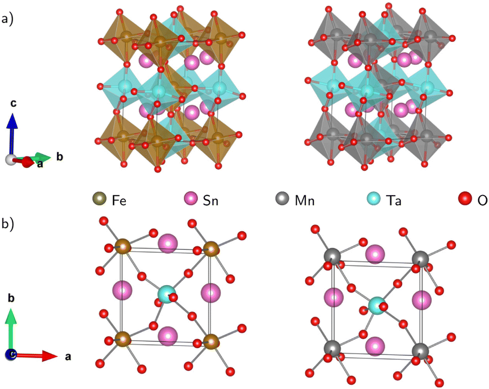 | ||
| Fig. 1 Schematic representation of the Sn2MnTaO6 and Sn2FeTaO6 double perovskites conventional unit cell in (a) polyhedral form and (b) top view of the atomic form. The deviation of B–O–B′ bond angles from 180° indicating significant buckling of the octahedral connection. The Jahn–Teller effect is responsible for the BO6 and B′O6 octahedra distortion resulting in B/B′–O bond length changes (see 〈ω〉 and Δd in Table 2). | ||
Calculating the octahedral factor μ and tolerance factor t, derived from simple geometrical principles, is an easy way to predict the basic formability of any new material with targeting perovskite structure based on chemical composition. The conditions proposed for these two parameters suggesting a stable perovskite structure are 0.410 < μ < 0.895 and 0.813 < t < 1.107.34–36
The tolerance factor t value gives an initial idea of the crystal structure type. The ideal cubic symmetry (space group Pmm) with B–O–B′ bonding angles of 180° is usually predictable when the value of t is close to unity (1.0 < t < 1.05). The deviation of t from 1.0 causes different crystal structures as for t > 1.05, a hexagonal symmetry (space group Rm) is expected. If 0.97 < t < 1.0, the DP compounds have a tetragonal symmetry (space group I4/m), whereas with a decreasing tolerance factor t < 0.97, the materials tend to crystallize into distorted perovskite structures such as an orthorhombic symmetry (space group Pnma or Pbnm) or a monoclinic symmetry (P21/n).25,37 The deviation from the cubic symmetry occurs due to the octahedral distortion, which is often accompanied by tension and compression in the three bonds A–O, B–O, and B′–O due to the mismatch compensated by tilting and rotation of BO6 and B′O6 octahedra. These distortions occur to obtain a more favourable configuration from the energetic point of view.
Using available ionic radii,38 our calculations gave the value of 0.46 and 0.89 for μ and t, respectively for SMTO and SFTO, which are within the recommended range for stable perovskite structures. Such a value for t is generally observed for significantly distorted perovskites.39 Since the Mn3+ and Fe3+ ions have identical ionic radii (0.645 Å), for the same cations of Sn and Ta at A and B′ sites, respectively, SMTO and SFTO DP have the same value of μ and t.
The calculated t values suggest distorted structures for our investigated compounds. The regularity of the octahedra distortion can be quantified using the octahedral bond-length distortion parameter that can be obtained as
 | (4) |
| Parameters | Sn2MnTaO6 | Sn2FeTaO6 |
|---|---|---|
| 〈Ta–O〉 | 2.07 | 2.09 |
| 〈Mn/Fe–O〉 | 2.28 | 2.17 |
| 〈ω〉 (Mn/FeO6) | 33.99 | 35.35 |
| 〈ω〉 (TaO6) | 34.20 | 35.56 |
| Δd (TaO6) × 10−3 | 2.91 | 5.23 |
| Δd (Mn/FeO6) × 10−3 | 1.43 | 1.37 |
| Eform | −3.35 | −7.62 |
To understand the thermodynamic stability of the studied DP systems, we calculated the formation energy Eform by calculating the energy difference of the DP structure and existing materials using the expression
| Eform(Sn2BTaO6) = Etot(Sn2BTaO6) − (2ESn + EB + ETa + 6EO). | (5) |
Our calculations yield Eform values of −3.35 and −7.62 eV for SMTO and SFTO, respectively. They are negative values, indicating potential stable structures and favoring the formation of the studied compounds.43–45
3.2 Magnetic properties
After ensuring the ground state crystal structure stability, we calculated the magnetic and electronic properties of the predicted compounds using the optimized structural information. As mentioned before, to capture the correct magnetic and electronic properties, it is crucial to include the electron–electron correction beyond GGA at Mn/Fe (3d) and Ta (5d) sites by applying Hubbard correction. We utilized spin-polarized DFT calculations with the GGA + U techniques to assess the magnetic and electronic properties of the chosen compounds. Here, we tested values of U = 4, 5 eV for Mn/Fe-3d and U = 1, 2 eV for Ta-5d. We note that the magnetic and electronic behavior do not strongly depend on the choice of U values, as there is a convergence for total magnetic moments and band gaps with respect to the U values. Therefore, for the sake of simplicity, we only show the results of U41 (UMn,Fe = 4 eV and UTa = 1 eV).To confirm the stable magnetic state of SMTO and SFTO DPs in their triclinic crystal phase, total energy calculation was performed in which we assume different magnetic ordering of FM, antiferromagnetic (AFM1, 2), and ferrimagnetic (FiM) by the spin alignments of the Mn/Fe and Ta ions Fig. 2. The total energy calculations show the stability of AFM2 state over FM state by a relatively small energy difference of 0.20 meV for SMTO, while the FM phase has the minimum energy for SFTO. Table 3 summarizes the calculated total energy differences between FM and AFM orderings (ΔE = EFM − EAFM), total and local magnetic moments for the investigated compounds. The Mn and Fe atoms dominate the magnetic behaviour, with magnetic moments of 5.03 μB and 3.98 μB in SMTO and SFTO, respectively. The zero-values for the total magnetic moments and local magnetic moments with different signs confirm that the Mn ions order antiferromagnetically with respect to the Ta ions in SMTO. The Mn1 spin moment is completely compensated by the Mn2 spin moment. In contrast, the magnetic moments of Fe and Ta are parallel in SFTO. From the formability point of view, the charge balance between cations and anions must be maintained to form a perovskite structure. The calculated magnetic moments at Mn/Fe and Ta sites indicate the stabilization of nominal +3 and +5 states with d4/d5 and d0 occupancies, respectively, keeping the charge neutrality in the ionic picture of Sn2+2 (Mn/Fe)3+Ta5+O62−. It puts the transition metals in the electron configuration of Mn3+(3d4: t32g e1g), Fe3+(3d5: t32g e2g), and Ta5+: 5d0, resulting in an AFM superexchange between Mn-3d half-field states and a FM superexchange between Mn/Fe-3d half-field and Ta-5d empty orbitals following the Goodenough–Kanamori rule.46,47 The d-states of B (B′)-site cations split into low-energy t2g triplet and high-energy eg doublet subsets driven by the crystal field in the octahedral environment. In the +5-oxidation state, Ta-d states remain empty, and the small value of magnetic moment comes from the strong hybridization of Ta-5d with O-2p states.
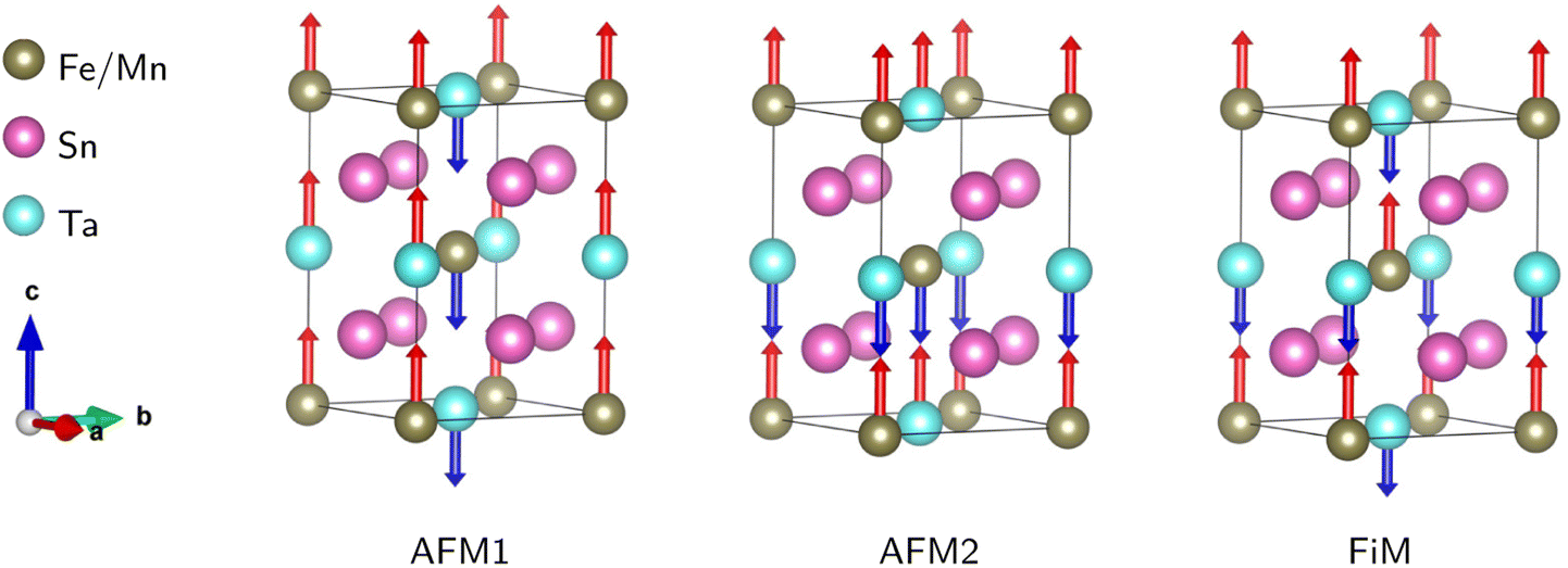 | ||
| Fig. 2 Different magnetic configurations of the conventional cell for the Sn2Mn/FeTaO6 DPs; AFM1, 2: antiferromagnetic; FiM: ferrimagnetic. Total energy calculations show that AFM2 and FM orderings are the magnetic ground states for SMTO and SFTO, respectively, resulting from a superexchange interaction between Mn/Fe-3d half-field and Ta-5d empty orbitals following the Goodenough–Kanamori rule. | ||
| Material | ΔEFM−AFM (eV) | Total magnetic moment (μB) | Local magnetic moments (μB) | Band gap (eV) | |
|---|---|---|---|---|---|
| ↑ | ↓ | ||||
| Sn2MnTaO6 | 0.0002 | 0.00 | mMn1 = 5.04, mTa1 = −0.03 | 1.02 | 1.17 |
| mMn2 = −5.02, mTa2 = 0.04 | |||||
| Sn2FeTaO6 | −0.02 | 8.00 | mFe1 = 3.99, mTa1 = 0.06 | 1.08 | 1.06 |
| mFe2 = 4.00, mTa2 = 0.07 | |||||
3.3 Electronic properties
We calculated the spin-polarized band structures along the high symmetry direction of BZ, total and partial DOS (PDOS) (Fig. 3). Both spin channels comprise band gaps, resulting in a semiconducting nature for both compounds. For SMTO, there are indirect band gaps for the spin-up and spin-down channels, of 1.02 eV and 1.17 eV, respectively, as the valence band maxima (VBM) and conduction band minima (CBM) are located at the V2 and T2 symmetry points of BZ, respectively. SFTO has the same behavior with indirect band gaps of 1.08 eV and 1.06 eV for the spin-up and spin-down channels, respectively (along the V2 → T2 path).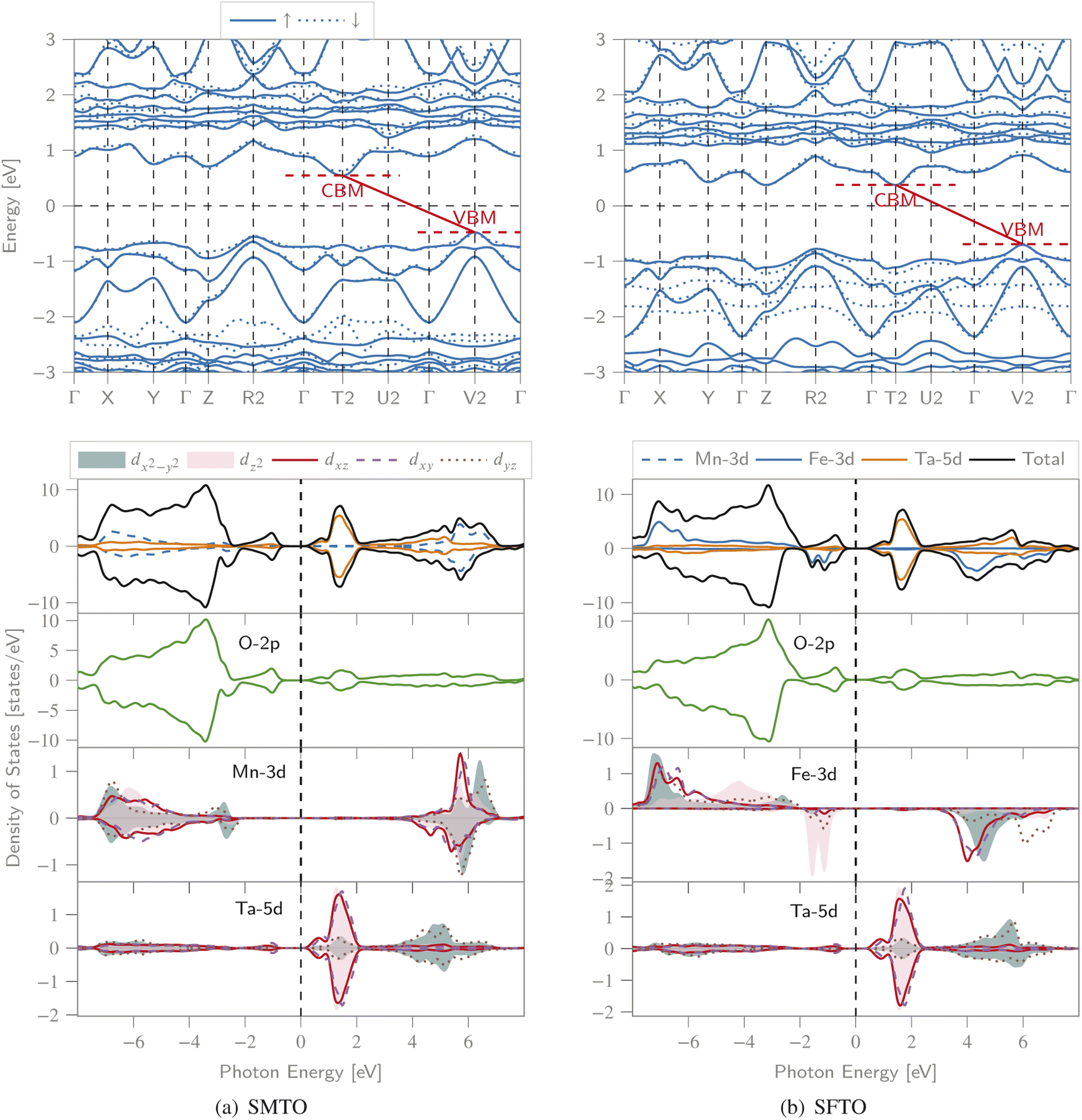 | ||
| Fig. 3 The spin polarized band structure (upper), total DOS and PDOS (lower) of the (a) SMTO and (b) SFTO compounds computed employing GGA + U, U41 approximation (UMn,Fe = 4.0 eV and UTa = 1.0 eV). The Fermi level is set as zero. CBM: conduction band minimum, VBM: valence band maximum. Both structures exhibit a semiconducting nature with band gaps slightly larger than 1.0 eV in both spin states, see Table 3 for details. | ||
For SMTO, we find that the most contribution in the valence band from −7.0 to −2.0 eV below the Fermi level comes from Mn-3d and O-2p states, while the Ta ion does not contribute significantly to PDOS in this region. Above the Fermi level, in the energy region between 0.0 and 2.0 eV, the Ta-5d states have the most contribution in the conduction band. In this energy region, the hybridization between O-2p and Ta-5d orbitals causes the non-centrosymmetric displacement of Ta5+ ions in their respective octahedra. Below the Fermi level, Ta-5d states are relatively empty, confirming the reported Ta5+: 5d0 electron configuration. An overlap between the Mn-3d and O-2p states extending from about −7.0 eV to −1.0 eV indicates the Mn–O covalent bonding. A similar behavior is observed for SFTO as in the range of −8.0 eV to −1.0 eV the valence band is mainly composed of O-2p and Fe-d orbitals. The Ta states contribute most significantly to the DOS near the Fermi level in the conduction band, between 0.0 and 2.0 eV.
Moreover, the symmetric DOS distribution for the spin-up and spin-down channels supports the AFM configuration for SMTO. For both SMTO and SFTO, in the range from −7.0 eV to −1.0 eV below the Fermi level and from 1.0 eV to 7.0 eV above the Fermi level, we observe an energy degeneracy for the p and d orbitals of oxygen and Mn(Fe)/Ta, respectively.
3.4 Electron charge density analysis
We calculated the electron charge density, to describe the chemical bonding associated with the SMTO and SFTO DPs and charge sharing between the atoms, using the GGA + U approximation. The charge density plots describe the charge distribution difference between the optimized and initial structures. They show the loss or gain of the electron on a specific atom, blue (−0.01) and red (+0.01) in the color contour, respectively (Fig. 4). The maximum density is located in the oxygen atoms' vicinity, due to their large electronegative nature. It can also be observed that Ta atoms lose more electrons compared to the Mn/Fe atoms, agreeing with the assigned +5 and +3 valence states, respectively. The shared electrons between oxygen and Mn/Fe and Ta atoms show the covalent nature of the Mn/Fe–O and Ta–O bonds. Furthermore, the overlapping Mn, Fe, Ta and O charge contours evidence the p–d hybridization. The non-spherical shapes of the transition metal atoms Mn/Fe and Ta indicate that the d states are partially filled. Moreover, Fig. 4 visualizes the distorted and tilted Mn/FeO6 and TaO6 octahedra.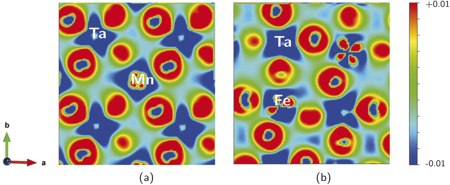 | ||
| Fig. 4 Charge density difference plots (e/Å3), describing the charge distribution difference between the optimized and initial structures, in (001) plane for (a) SMTO and (b) SFTO compounds. Positive (negative) values show the charge accumulated (depleted) regions. The charge sharing between the Mn/Fe–O and Ta–O atoms in Mn/FeO6 and TO6 octahedra show the covalent nature, and p–d hybridization. | ||
3.5 Optical properties
Revealing the optical properties of materials is essential to predict their possible application and device performance in optoelectronics and PVs. The optical response of matter can be described by the frequency-dependent complex dielectric function, visualizing the optical transition between the occupied and unoccupied orbitals (see Section 2 for details).To obtain a deeper insight into the electronic band profile, and to analyse the optical behaviour, including the dielectric functions and absorption coefficients, we calculated the spin-polarized optical parameters for the SMTO and SFTO DPs, using the GGA + U method (UMn,Fe = 4.0 eV and UTa = 1.0 eV). Due to the studied compounds' asymmetric geometrical structure, we calculated the optical properties along x-, y- and z-directions. Our results, however, revealed identical values in different directions, not revealing any significant anisotropy. Hence, here we only represent the optical properties along the x-axis. The calculated spin-dependent real and imaginary dielectric constants, functions of energy in the energy range of 0.0 eV to 8.0 eV above the Fermi level, are plotted in Fig. 5(a). A material behaves as a dielectric for ε1 > 0 and as a metal for ε1 < 0. In Fig. 5, SMTO represents a similar dielectric behavior for the spin up and down channels due to its AFM nature. The value of the real dielectric function at zero energy shows the static dielectric constant ε1(0) that explains the reverse relation between the semiconductor band gap as ε1(0) = 1 + (ℏω/Eg)2 (ref. 49). Therefore, the higher value of ε1(0) reveals a smaller band gap. For SMTO, the spin up channel has a slightly higher value of ε1(0) than the spin down channel indicating a lower band gap value as reported in Table 3. The imaginary dielectric constant is small (nearly zero) for both compounds up to certain energy. The peaks in the imaginary part of the dielectric function reveal the interband transition from the valence bands to the respective conduction bands. In SMTO and SFTO systems, the imaginary dielectric function has three main peaks at around 1.5, 2.5, and 4.5 eV. The low energy peaks are associated with the transition between the O-2p valence and the Ta-5d conduction bands. While the transition between O-2p valence band and Mn/Fe-3d conduction band caused the peaks located in higher energies. The first peak in ε2 of both compounds at 1.5 eV is attributed to the transitions from O-2p in the energy range of −1.5 to −0.5 eV to the first small peak of Ta-5d exactly above the Fermi level in the range 0.5 to 1 eV. The second peak at energy 2.5 eV in the ε2 diagram, which is stronger than the first one, is ascribed to the transitions from O-2p in the energy range of −1.5 to −0.5 eV to a strong Ta-5d peak in the energy range of 1.0 to 2.0 eV in the DOS. A significant difference between the two materials is the presence of additional Fe-3d states in the spin down channel of SFTO in the energy range between −2.0 and −1.0 eV, causing the additional electron transitions to O-2p states above the Fermi level. It gives rise to a stronger contribution of the spin down channel in the ε2 curve compared to the spin up channel at the energy ∼3.0 eV in SFTO. To investigate the visible-light harvesting capacity, we calculated the DPs' absorption coefficients, and display them alongside the AM1.5g solar irradiance reference spectrum48 (Fig. 5(b)). The absorption coefficient is zero when the energy is in the range of 0.0–1.0 eV, and there is no electric transition because the photon energy is below the SMTO and SFTO band gaps (∼1.0 eV). For a photon energy larger than the band gap value (∼1.0 eV), the absorption coefficient increases, reaching the first peak with the value of around 0.5 × 105 cm−1 at 1.8 eV. The secondary peak appears at the 2.5–3.0 eV energy range, with an absorption coefficient value of 2.0 × 105 cm−1. The absorption spectrum increases with increasing photon energy, after around 4.0 eV. The α value in the visible region is in the order of 105 cm−1, confirming that SMTO and SFTO are promising candidates for PV applications.50,51
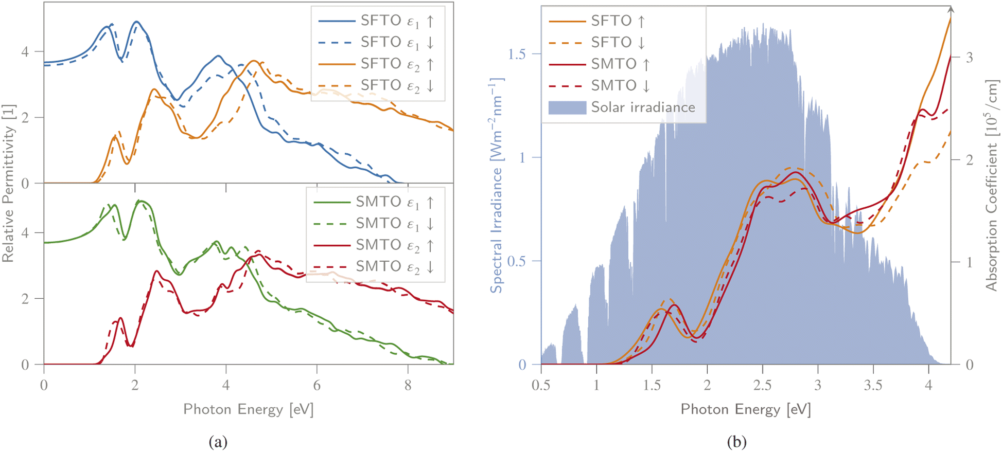 | ||
| Fig. 5 (a) Spin-dependent real ε1 and imaginary ε2 parts of dielectric function, (b) absorption spectra, as a function of photon energy calculated for SMTO and SFTO systems using GGA + U, together with the AM1.5g solar irradiance spectrum.48 All spin states exhibit a non-vanishing absorption behaviour within a wide, PV-relevant spectral range between 1.3 and 4.2 eV. | ||
4 Conclusions
We performed DFT calculations to study the crystal structure, electronic, magnetic, and optical properties of SMTO and SFTO DPs. Our structural optimizations, using total energy calculations under the GGA-PBE scheme, indicate triclinic crystal structures for both compounds, with significant polar distortions of BO6 and B′O6 originating from the JT effect. Negative formation energies furthermore assure their thermodynamic stability. We studied the magnetic, electronic, and optical properties with the GGA + U method. The magnetic phase stability of SMTO and SFTO in different magnetic configurations has also been discussed, and an AFM and FM nature was predicted to be their magnetic ground states, respectively. We showed that these materials have a semiconductor behavior with an energy gap of around 1 eV according to the density of state calculations. The optical properties, including the dielectric functions and absorption coefficients, were studied. The structural stability, suitable band gap, and absorption coefficient values of studied compounds suggest they could be good candidates for PV applications.Conflicts of interest
There are no conflicts to declare.Acknowledgements
The computational calculations contributing to this work were carried out with support of the UCloud Services provided by the eScience Center at SDU.Notes and references
- S. Y. Yang, L. W. Martin, S. J. Byrnes, T. E. Conry, S. R. Basu, D. Paran, L. Reichertz, J. Ihlefeld, C. Adamo, A. Melville, Y.-H. Chu, C.-H. Yang, J. L. Musfeldt, D. G. Schlom, J. W. Ager and R. Ramesh, Appl. Phys. Lett., 2009, 95, 062909 CrossRef.
- S. Y. Yang, J. Seidel, S. J. Byrnes, P. Shafer, C. H. Yang, M. D. Rossell, P. Yu, Y. H. Chu, J. F. Scott, J. W. Ager, L. W. Martin and R. Ramesh, Nat. Nanotechnol., 2010, 5, 143–147 CrossRef CAS PubMed.
- R. Nechache, C. Harnagea, A. Pignolet, F. Normandin, T. Veres, L.-P. Carignan and D. Ménard, Appl. Phys. Lett., 2006, 89, 102902 CrossRef.
- W. Huang, C. Harnagea, D. Benetti, M. Chaker, F. Rosei and R. Nechache, J. Mater. Chem. A, 2017, 5, 10355–10364 RSC.
- Arti, S. Kumar, P. Kumar, R. Walia and V. Verma, Results Phys., 2019, 14, 102403 CrossRef.
- S. Halder, T. K. Bhowmik, A. Dutta and T. Sinha, Ceram. Int., 2020, 46, 21021–21032 CrossRef CAS.
- L. Fang, L. You, Y. Zhou, P. Ren, Z. Shiuh Lim and J. Wang, Appl. Phys. Lett., 2014, 104, 142903 CrossRef.
- M. Alexe and D. Hesse, Nat. Commun., 2011, 2, 256 CrossRef.
- Y.-T. Peng, S.-H. Chiou, C.-H. Hsiao, C. H. Ouyang and C.-S. Tu, Sci. Rep., 2017, 7, 45164 CrossRef CAS.
- R. Nechache, C. Harnagea, S. Licoccia, E. Traversa, A. Ruediger, A. Pignolet and F. Rosei, Appl. Phys. Lett., 2011, 98, 202902 CrossRef.
- R. Nechache, C. Harnagea, S. Li, L. Cardenas, W. Huang, J. Chakrabartty and F. Rosei, Nat. Photonics, 2015, 9, 61–67 CrossRef CAS.
- R. Gupta, M. Tomar, A. Kumar and V. Gupta, Smart Mater. Struct., 2017, 26, 035002 CrossRef.
- V. F. Freitas, E. A. C. Astrath, L. C. Dias, M. Mazur, G. B. Souza, T. G. M. Bonadio, J. A. Eiras, D. M. Silva, J. H. Rohling, G. S. Dias, L. F. Cótica and I. A. Santos, Braz. J. Phys., 2021, 51, 1215–1223 CrossRef CAS.
- Z. Pan, J. Chen, R. Yu, L. Patra, P. Ravindran, A. Sanson, R. Milazzo, A. Carnera, L. Hu, L. Wang, H. Yamamoto, Y. Ren, Q. Huang, Y. Sakai, T. Nishikubo, T. Ogata, X. Fan, Y. Li, G. Li, H. Hojo, M. Azuma and X. Xing, Chem. Mater., 2019, 31, 1296–1303 CrossRef CAS.
- J. M. Soler, E. Artacho, J. D. Gale, A. García, J. Junquera, P. Ordejón and D. Sánchez-Portal, J. Phys.: Condens. Matter, 2002, 14, 2745–2779 CrossRef CAS.
- P. Ordejón, E. Artacho and J. M. Soler, Phys. Rev. B: Condens. Matter Mater. Phys., 1996, 53, R10441–R10444 CrossRef PubMed.
- J. P. Perdew, K. Burke and M. Ernzerhof, Phys. Rev. Lett., 1996, 77, 3865–3868 CrossRef CAS PubMed.
- H. J. Monkhorst and J. D. Pack, Phys. Rev. B: Solid State, 1976, 13, 5188–5192 CrossRef.
- Y.-S. Kim, C.-H. Ri, U.-H. Ko, Y.-H. Kye, U.-G. Jong and C.-J. Yu, ACS Appl. Mater. Interfaces, 2021, 13, 14679–14687 CrossRef CAS PubMed.
- C.-J. Yu, Y.-H. Kye, U.-G. Jong, K.-C. Ri, S.-H. Choe, J.-S. Kim, S.-G. Ko, G.-I. Ryu and B. Kim, ACS Appl. Mater. Interfaces, 2020, 12, 1858–1866 CrossRef CAS PubMed.
- W. Li, S. Sidhik, B. Traore, R. Asadpour, J. Hou, H. Zhang, A. Fehr, J. Essman, Y. Wang, J. M. Hoffman, I. Spanopoulos, J. J. Crochet, E. Tsai, J. Strzalka, C. Katan, M. A. Alam, M. G. Kanatzidis, J. Even, J.-C. Blancon and A. D. Mohite, Nat. Nanotechnol., 2022, 17, 45–52 CrossRef CAS.
- A. I. Liechtenstein, V. I. Anisimov and J. Zaanen, Phys. Rev. B: Condens. Matter Mater. Phys., 1995, 52, R5467–R5470 CrossRef CAS.
- M. M. Saad H.-E., J. Alloys Compd., 2014, 587, 652–658 CrossRef CAS.
- P. Sanyal, A. Halder, L. Si, M. Wallerberger, K. Held and T. Saha-Dasgupta, Phys. Rev. B, 2016, 94, 035132 CrossRef.
- A. Halder, D. Nafday, P. Sanyal and T. Saha-Dasgupta, npj Quantum Mater., 2018, 3, 17 CrossRef.
- H. A. Kramers, Atti del Congresso Internazionale dei Fisici, 1927, vol. 2, pp. 545–557 Search PubMed.
- R. de L. Kronig, J. Opt. Soc. Am., 1926, 12, 547–557 CrossRef CAS.
- M. Altarelli and D. Y. Smith, Phys. Rev. B: Solid State, 1974, 9, 1290–1298 CrossRef CAS.
- K. Liu, H. Fan, P. Ren and C. Yang, J. Alloys Compd., 2011, 509, 1901–1905 CrossRef CAS.
- A. Siad, M. Baira, F. Z. Dahou, K. Bettir and M. E. A. Monir, J. Solid State Chem., 2021, 302, 122362 CrossRef CAS.
- H. Fuh, Y. Liu, S. Chen and Y. Wang, J. Alloys Compd., 2013, 547, 126–131 CrossRef CAS.
- N. Rahmani, M. Ghazi, M. Izadifard and B. Sanyal, J. Magn. Magn. Mater., 2021, 519, 167492 CrossRef CAS.
- N. Rahmani, M. E. Ghazi, M. Izadifard, D. Wang, A. Shabani and B. Sanyal, J. Phys.: Condens. Matter, 2019, 31, 475501 CrossRef CAS PubMed.
- P. R. Varadwaj, Phys. Chem. Chem. Phys., 2020, 22, 24337–24350 RSC.
- C. J. Bartel, C. Sutton, B. R. Goldsmith, R. Ouyang, C. B. Musgrave, L. M. Ghiringhelli and M. Scheffler, Sci. Adv., 2019, 5, eaav0693 CrossRef CAS PubMed.
- C. J. Bartel, J. M. Clary, C. Sutton, D. Vigil-Fowler, B. R. Goldsmith, A. M. Holder and C. B. Musgrave, J. Am. Chem. Soc., 2020, 142, 5135–5145 CrossRef CAS PubMed.
- J. B. Philipp, P. Majewski, L. Alff, A. Erb, R. Gross, T. Graf, M. S. Brandt, J. Simon, T. Walther, W. Mader, D. Topwal and D. D. Sarma, Phys. Rev. B: Condens. Matter Mater. Phys., 2003, 68, 144431 CrossRef.
- R. D. Shannon, Acta Crystallogr., Sect. A: Cryst. Phys., Diffr., Theor. Gen. Crystallogr., 1976, 32, 751–767 CrossRef.
- M.-R. Li, P. W. Stephens, M. Retuerto, T. Sarkar, C. P. Grams, J. Hemberger, M. C. Croft, D. Walker and M. Greenblatt, J. Am. Chem. Soc., 2014, 136, 8508–8511 CrossRef CAS PubMed.
- N. Rahmani, M. E. Ghazi, M. Izadifard, A. Shabani and J. Adam, Phys. Chem. Chem. Phys., 2021, 23, 19571–19578 RSC.
- H. A. Jahn and E. Teller, Proc. R. Soc. London, Ser. A, 1937, 161, 220–235 CAS.
- J. A. Alonso, M. J. Martínez-Lope, M. T. Casais and M. T. Fernández-Díaz, Inorg. Chem., 2000, 39, 917–923 CrossRef CAS PubMed.
- N. Noor, M. W. Iqbal, T. Zelai, A. Mahmood, H. Shaikh, S. M. Ramay and W. Al-Masry, J. Mater. Res. Technol., 2021, 13, 2491–2500 CrossRef CAS.
- T. Ghrib, A. Rached, E. Algrafy, I. A. Al-nauim, H. Albalawi, M. Ashiq, B. U. Haq and Q. Mahmood, Mater. Chem. Phys., 2021, 264, 124435 CrossRef CAS.
- Q. Mahmood, M. Alhossainy, M. Rashid, T. H. Flemban, H. Althib, T. Alshahrani, M. Rashid and A. Laref, Mater. Sci. Eng. B, 2021, 266, 115064 CrossRef CAS.
- J. B. Goodenough, J. Phys. Chem. Solids, 1958, 6, 287–297 CrossRef CAS.
- J. Kanamori, J. Phys. Chem. Solids, 1959, 10, 87–98 CrossRef CAS.
- N.R.E. Laboratory, Reference Air mass 1.5 spectra, https://www.nrel.gov/grid/solar-resource/spectra-am1.5.html, 2022, accessed on 29 September 2022.
- D. R. Penn, Phys. Rev., 1962, 128, 2093–2097 CrossRef CAS.
- Y. Wang, Y. Zhang, P. Zhang and W. Zhang, Phys. Chem. Chem. Phys., 2015, 17, 11516–11520 RSC.
- X. Qiu, B. Cao, S. Yuan, X. Chen, Z. Qiu, Y. Jiang, Q. Ye, H. Wang, H. Zeng, J. Liu and M. Kanatzidis, Sol. Cells, 2017, 159, 227–234 CrossRef CAS.
| This journal is © The Royal Society of Chemistry 2022 |