
 Open Access Article
 This Open Access Article is licensed under a Creative Commons Attribution-Non Commercial 3.0 Unported Licence
Prediction of the electronic structure of single-walled GeS nanotubes
Deyang Yu†
abf,
Ruiqi Ku†be,
Yangyang Hu ac,
Yadong Weibe,
Cuancuan Zhub,
Zhongli Liue,
Guiling Zhang*ac,
Weiqi Li*bde,
Jianqun Yang*e and
Xingji Li*e
ac,
Yadong Weibe,
Cuancuan Zhub,
Zhongli Liue,
Guiling Zhang*ac,
Weiqi Li*bde,
Jianqun Yang*e and
Xingji Li*e
aSchool of Materials Science and Chemical Engineering, Harbin University of Science and Technology, Harbin 150080, China. E-mail: guiling-002@163.com
bSchool of Physics, Harbin Institute of Technology, Harbin 150001, China
cKey Laboratory of Green Chemical Technology of College of Heilongjiang Province, Harbin University of Science and Technology, Harbin 150080, China
dKey Lab of Micro-Optics and Photonic Technology of Heilongjiang Province, Harbin 150001, China
eTechnology Innovation Center of Materials and Devices at Extreme Environment, Harbin 150001, China. E-mail: tccliweiqi@hit.edu.cn; yangjianqun@hit.edu.cn; lxj0218@hit.edu.cn
fDepartment of Radiation Physics, Harbin Medical University Cancer Hospital, Harbin 150081, China
First published on 13th October 2022
Abstract
The structure and electronic properties of puckered GeS nanotubes have been investigated using first-principles density functional theory calculation. Our results show that both the armchair and zigzag GeS nanotubes are semiconductor materials with an adjustable band gap. The band gap increases gradually with increasing the tube diameter, and slowly converges to the monolayer limit. On the application of strain, the GeS nanotubes provide interesting strain-induced band gap variation. When the compressive strain reached 20%, zigzag GeS nanotubes are completely transformed into armchair GeS nanotubes. In addition, the elastic properties of the relatively stable armchair GeS nanotubes have been studied, the Young's modulus of the armchair (11, 11), (13, 13) and (15, 15) nanotubes were calculated to be 227.488 GPa, 211.888 GPa and 213.920 GPa, respectively. Our work confirms that compared with carbon nanotubes, two-dimensional materials with a puckered structure are easier to realize phase transition by stress.
Introduction
Since the discovery of graphene in 2004,1 two-dimensional (2D) materials have attracted great research interest in nanoelectronic devices due to their unique structural and electronic properties.2–4 Although 2D monolayer materials show unique physical and electronic properties, the nanotubes (NTs), a kind of one-dimensional (1D) material, exhibit special mechanical and magnetic properties as a result of quantum confinement effects.5 In the past few years, the experimental and theoretical exploration of various nanotubes has opened a promising new field in condensed matter physics and chemistry. For example, Iijima et al. firstly discovered and synthesized carbon nanotubes (CNTs) in the early 1990s.6,7 CNTs have excellent properties such as high tensile strength, ultra-light weight, special electronic structures and high chemical and thermal stability.8,9 Inspired by the discovery of CNTs, BN nanotubes (BNNTs) were synthesized in 1995 by Chopra et al.10 BNNTs display different physical properties from CNTs such as a wide bandgap which is larger than 6.0 eV, extraordinary heat resistance, good transparency and thermal neutron adsorption ability.11,12 Later, nanotubes of other inorganic materials such as silicon nanotubes,13 MoS2 nanotubes14 and GaSe nanotubes15 were observed and successfully synthesized. The superior properties of these nanotubes provided a wide range of potential applications including biomolecules, drugs, biosensor diagnostic and analysis, photovoltaics, microelectronics, gas sensing, and infrared photoelectric detection.16–19Recently, 2D GeS has aroused extensive research interest from theory to experiment owing to its earth-abundant, environmental compatibility and outstanding electronic performances. Experimentally, 2D GeS nanosheets were successfully synthesized using one-pot method20 and vapor deposition processes.21 It is a layered p-type semiconductor with a distorted rock-salt orthorhombic structure and a band gap of 1.65 eV.22,23 Theoretically, Zhang et al. reported that the band gaps of GeS monolayer are rather sensitive to the external electric field, and the band gaps present an approximately linear increase under strain from −10% to 10%.24 Xu and co-workers have predicted angular and strain dependence of effective masses of the GeS monolayer from the first-principles calculations.25 Monolayer GeS shows a variety of quite extraordinary properties including high carrier mobility of 3680 cm2 V−1 s−1,26 tunable electronic properties via external electric fields and strains,24 anisotropic features27 and giant piezoelectric effects.28 These charming properties of 2D GeS make it to be promising applications in high-efficiency solar cells, selective gas sensing, high-sensitivity photodetectors and larger piezoelectric coefficients devices.29–31
In the research of 1D GeS, Lan et al. have synthesized the single-crystalline GeS nanoribbons by chemical vapor deposition method and explored the photoresponse properties.32 Theoretically, Li et al. reported that GeS nanoribbons (GeSNRs) with armchair and zigzag edges are semiconductors and metals, respectively. And the hydrogen-terminated GeSNRs exhibited semiconducting properties no matter their edges are armchair or zigzag.33 Su and co-workers reported that H-terminated armchair GeSNRs exhibit large in-plane polarization along the ribbon direction which converges to the value of 2D GeS as the width increases.34 Although the 2D monolayer and 1D nanoribbon of GeS have been extensively studied in recent years. As far as we know, the structure and electronic properties of GeS nanotubes have not been studied before. In most two-dimensional materials such as carbon and BN nanosheets, nanotubes can be formed by rolling up two-dimensional sheets. In this work, we performed calculations based on first-principles methods to predict the structure and electronic properties of GeS nanotubes in armchair and zigzag directions by rolling up corresponding nanosheets. The optimization of single-walled nanotubes (SWNTs) networks and the detailed understanding of their electronic properties are given to offer considerable scope for the development of GeS nanotube-based electronics and to have important implications for next-generation optoelectronic devices.
Calculation details
The smallest structural units of armchair and zigzag GeS nanotubes with different diameters were created. All of the first-principles calculations were carried out based on density functional theory (DFT) using the Vienna Ab initio Simulation package (VASP)35 and the projection augmented wave (PAW) method.36 Atomic relaxation was performed under the generalized gradient approximation (GGA) Perdew–Burke–Ernzerhof (PBE) exchange-correlation functional,37 and the electronic structure calculation used a cutoff energy of 450 eV and a k-point grid of 1 × 1 × 17. The geometry optimizations were performed by the conjugated gradient method, and the convergence threshold was set to be 10−4 eV in energy and 0.02 eV Å−1 in force. A vacuum layer of 15 Å was set in the aperiodic direction to avoid the interaction between the nearest neighboring cells. Elastic properties of GeS nanotubes were predicted using our house code, and the computational details of mechanical properties can be found in previous work.38Results and discussion
The atomic structure of monolayer GeS after relaxation is depicted in Fig. 1(a). The calculated lattice constants are a = 3.664 Å, b = 4.464 Å, which are in good agreement with theoretical data39,40 and experimental value.41 In addition, our calculations for Ge–S bond lengths and bond angles are d1 = 2.427 Å, d2 = 2.473 Å, θ1 = 94.602°, θ2 = 103.898°, respectively, they are very close to previous works.39,42 Nanotubes are built by rolling up monolayer GeS along with the armchair and zigzag directions, which can be denoted as armchair (n, n) and zigzag (n, 0) according to the definition used in carbon nanotubes.43 The optimized GeS nanotubes displayed in Fig. 1(b) and (c), respectively. As shown in Table 1, after curling from two-dimensional planar structure to nanotubes, arrangement of the inner and outer atoms as well as structural parameters is determined by the angle between the chemical bond and the curl vector. For zigzag nanotubes, the bond length d2 in the inner layer slightly decreases from 2.473 Å to 2.419 Å, whereas that of the outer layer is stretched to 3.917 Å. However, the change of bond lengths for armchair nanotubes are almost negligible. The changes of bond angles θ1 and θ2 from monolayer to nanotubes are also that zigzag is larger than armchair nanotubes. | ||
| Fig. 1 Geometric structures of (a) monolayer GeS, (b) armchair (11, 11), (19, 19) GeS nanotubes and (c) zigzag (11, 0), (19, 0) GeS nanotubes. | ||
| Diameter (Å) | Bond length (Å) | Bond angle (°) | |||||||
|---|---|---|---|---|---|---|---|---|---|
| Inner | Outer | Inner | Outer | ||||||
| d1 | d2 | d1 | d2 | θ1 | θ2 | θ1 | θ2 | ||
| Monolayer | 2.427 | 2.473 | 2.427 | 2.473 | 94.602 | 103.898 | 94.602 | 103.898 | |
![[thin space (1/6-em)]](https://www.rsc.org/images/entities/char_2009.gif) |
|||||||||
| Armchair | |||||||||
| (11, 11) | 14.018 | 2.427 | 2.442 | 2.427 | 2.460 | 95.272 | 119.541 | 92.742 | 102.345 |
| (13, 13) | 16.802 | 2.427 | 2.446 | 2.427 | 2.461 | 95.192 | 117.128 | 92.971 | 102.151 |
| (15, 15) | 19.502 | 2.427 | 2.452 | 2.427 | 2.465 | 95.187 | 114.472 | 93.293 | 101.403 |
| (17, 17) | 22.370 | 2.427 | 2.451 | 2.427 | 2.464 | 95.155 | 113.567 | 93.362 | 101.622 |
| (19, 19) | 25.202 | 2.427 | 2.452 | 2.427 | 2.465 | 95.128 | 112.494 | 93.501 | 101.705 |
|
|||||||||
| Zigzag | |||||||||
| (11, 0) | 11.378 | 2.361 | 2.430 | 2.361 | 3.917 | 88.088 | 83.923 | 70.760 | 72.135 |
| (13, 0) | 13.560 | 2.377 | 2.422 | 2.377 | 3.793 | 88.558 | 84.889 | 70.338 | 71.736 |
| (15, 0) | 15.792 | 2.389 | 2.420 | 2.389 | 3.722 | 89.213 | 86.028 | 69.884 | 71.217 |
| (17, 0) | 17.980 | 2.398 | 2.419 | 2.398 | 3.654 | 89.408 | 86.606 | 69.614 | 70.853 |
| (19, 0) | 20.294 | 2.400 | 2.423 | 2.400 | 3.626 | 90.162 | 87.588 | 69.270 | 70.433 |
The diameter of GeS nanotubes is one of the most important parameters that determines the morphology of the nanotubes and further affects their physical properties. As shown in Fig. 2, the armchair and zigzag GeS nanotubes are a type of semiconductor materials. The band gap of the GeS nanotubes increases with the diameter, which is similar to that of BN, black phosphorus and MoS2 nanotubes,44–47 and this is attributed to the strong axial polarization along the tube axis.48 The calculated band gaps of different armchair and zigzag nanotubes are in 1.579 eV – 1.724 eV and 1.490 eV – 1.620 eV, respectively. The band gaps are very close to the precious first-principles predictions42,49 and experimental results20 of the 2D GeS band gap with 1.65 and 1.58 eV. It is also found that the band gap of zigzag nanotube increases gradually with increasing the size, on the other hand, the band gap of armchair nanotubes with odd units is larger than that of nanotubes with even units. The PBE functional is widely used in the band gap prediction for various systems, including the nanotube system.47,50,51 It is well known that the PBE method underestimates the band gap, and that the Heyd–Scuseria–Ernzerhof (HSE) functional gives more accurate values.52 However, the correlative computed results of both methods can be used to qualitatively estimate the various electronic behaviors. For the case of the GeS nanotubes with small tube diameter, we have calculated its band gap using both functionals. As expected, the band gaps calculated with PBE functional are 1.49 eV, 1.50 eV, 1.58 eV and 1.63 eV for zigzag (11, 0), (13, 0) nanotubes and armchair (11, 11), (13, 13) nanotubes, respectively. And the band gap values of that calculated with HSE functional are 2.16 eV, 2.17 eV, 2.33 and 2.38 eV. The results show that the band gaps predicted by HSE functional are larger than that of PBE functional, but the relationship between band gap and diameter of GeS nanotubes is completely consistent.
 | ||
| Fig. 2 The band gap of armchair and zigzag tubes as a function of n. | ||
The partial charge density of the conduction band minimum (CBM) and valence band maximum (VBM) states at the Γ point in armchair and zigzag nanotubes are presented in Fig. 3, the CBM and VBM orbitals of armchair nanotubes are located at both the outer and inner atoms. However, the CBM and VBM orbitals of zigzag nanotubes are mainly located at the inner atoms. When the tubes size are reduced, both the CBM and VBM orbitals of armchair and zigzag nanotubes become more populated. It is known that its curvature generally reduces the distance between neighboring sites, especially along the circumference to a certain extent when rolling up the sheet into a tube. What's more, the respective charge densities of zigzag nanotubes start to overlap inside the cylinder. Our calculated results are in good agreement with previous reports of single-walled black phosphorus and LiF nanotubes.46,53 It is very interesting that the charges of CBM and VBM are not evenly distributed on the zigzag GeS tubes with large radius such as (11, 0), (15, 0) and (19, 0), but complementary. They are easy to form excitons with electron hole space separation after receiving photons, which can be applied to photodetectors, etc.
 | ||
| Fig. 3 Partial charge density distribution at Γ point of the CBM and VBM for the armchair and zigzag nanotube. The isosurface value is set to be 0.0005 e Å−3. | ||
Applying mechanical strain is an effective way to modulate the electronic properties of materials, the strain is defined as (C–C0)/C0, where C0 is the unit cell length of the unstrained nanotube. So the positive or negative value indicates the tensile or compressive strain. As shown in Fig. 4, the band structures of the armchair (11, 11) nanotubes in the strain range of −8% to 3% are indirect band gaps, and the indirect band gap is transformed to the direct band gap when the tensile strain reaches 4% to 8%. Fig. 5 shows zigzag (11, 0) nanotubes in the strain range of −6% to 5% are indirect band gaps, and the band gap transforms into a direct band gap when the tensile strain reaches 6%. For the strain applied along the armchair (11, 11) in Fig. 6(a), the band gap is initially increased with tensile strain from a value of 1.579 eV for the relaxed structure and reached the maximal value of 1.674 eV at +4% strain, then drops rapidly with further increased expansion. On the side of negative strain, the values of band gaps decrease monotonically from 1.458 eV to 1.241 eV in the strain range of −1% to −8%. Fig. 6(b) presents the band gap as a function of strain applied in the zigzag (11, 0). The band gap decreases monotonically from 1.490 eV to 1.366 eV with the tensile strain from 0% to 8%. For the compressive strain, the band gap reaches the maximal value of 1.500 eV at −1% strain, then decreases with further increased compression.
 | ||
| Fig. 4 Band structure of armchair (11, 11) nanotubes in the strain range of −8% to 8%. | ||
 | ||
| Fig. 5 Band structure of zigzag (11, 0) nanotubes in the strain range −6% to 6%. | ||
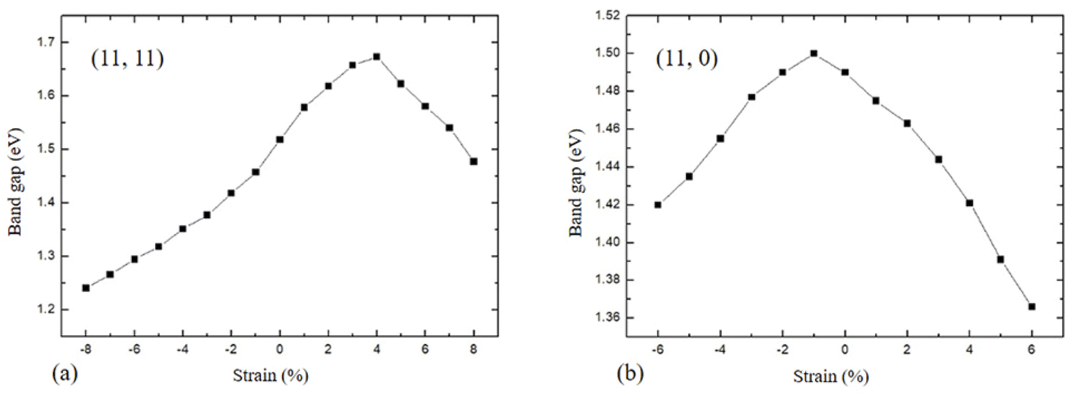 | ||
| Fig. 6 Variation of band gap as a function of strain for (a) the armchair (11, 11) and (b) zigzag (11, 0) GeS nanotubes. | ||
Theoretical54 and experimental55 works reported that the band gap of CNTs changes can range between ±100 meV per 1% stretch, depending on nanotube chirality. In addition, Minot et al. reported that strain can open a band gap in a metallic carbon nanotube and modify the band gap in a semiconducting carbon nanotube.55 Molecular-dynamics simulations of single-walled CNTs under tensile strain have shown, under certain conditions, breaking strains as large as 30–40%.56 In this work, the zigzag (11, 0) GeS nanotubes deformed when the compressive strain was larger than 6%. The lowest value of deformation energy occurs when the compressive strain continued to increase to 20%, as shown in Fig. 7(a), and the zigzag (11, 0) nanotubes completely transformed into armchair (11, 11) nanotubes. Similarly, as shown in Fig. 7(b) and (c), the zigzag (13, 0) and (15, 0) nanotubes are transformed into armchair nanotubes when the compressive strain reached 20%. Whereas, the structures of armchair (11, 11) nanotube remain intact without any bond breaking within the strain of −8% to 8%, which demonstrates the large elastic range of armchair GeS nanotubes. N. A. Poklonski et al. reported that the first order deformation structure phase transition is revealed at the critical uniaxial elongation 9% for the (6, 0) CNT57 and 5% for the (5, 5) CNT.58 It is well known that the puckered structures such as black phosphorus can bear high strain without breaking the structure by changing their puckering angle. Therefore, the armchair GeS nanotube can bear high strain due to the puckered structure in the armchair direction. This result suggests that armchair GeS nanotubes with lower energy are the optimal structures.
 | ||
| Fig. 7 Strain energy diagrams of (a) zigzag (11, 0), (b) (13, 0) and (c) zigzag (15, 0) nanotubes. | ||
The different performance between armchair and zigzag GeS nanotubes under strain indicate that the chirality has a significant influence on the mechanical properties of GeS nanotubes. Additionally, these significant changes suggest that applying strain can modulate the electronic properties of GeS nanotubes effectively. Thus, these results would provide a simple and effective route to tune the electronic properties of GeS nanotubes over a wide range and also facilitate the design of GeS nanotube devices.
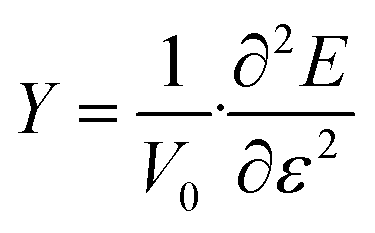
Finally, the Young's modulus is calculated to investigate the elastic properties of GeS nanotubes. Young's modulus, which indicates how much resistance the nanotube presents to its deformation under uni-axial strain, is defined as the second derivative of strain energy with respect to the strain at equilibrium configuration,59
 | ||
| Fig. 8 Strain energy diagrams of armchair (11, 11), (13, 13) and (15, 15) nanotubes. | ||
Conclusion
In summary, the results of this study show that the armchair and zigzag GeS nanotubes are semiconductor materials with adjustable band gaps, and the band gaps monotonically increase with the diameters of nanotubes. The band gaps of GeS nanotubes show abundant changes when a certain strain is applied in the axial direction of the nanotubes, indicating that GeS nanotubes are a stress-sensitive material. The structure of zigzag GeS nanotubes are greatly affected by different stresses, when the compressive strain on the surface of the structure reaches about 20%, the zigzag GeS nanotubes completely transform into armchair GeS nanotubes. For the relatively stable armchair GeS nanotubes, we further study their elastic properties, the Young's modulus of armchair (11, 11), (13, 13) and (15, 15) nanotubes were calculated to be 227.488 GPa, 211.888 GPa and 213.920 GPa, respectively. These simulation results not only reveal the tube diameter and strain effects on the electronic structures of GeS nanotube, but also contribute to the future use of the GeS nanotube in electronic devices.Author contributions
D. Y., R. K., C. Z. and Z. L. performed the calculations and the initial data analysis. D. Y. wrote the first draft of the manuscript. Y. H., Y. W., W. L., J. Y. and X. L. performed additional analysis, interpretations, and writing of the manuscript. G. Z. and W. L. supervised and guided the work.Conflicts of interest
There are no conflicts to declare.Acknowledgements
This work is financially supported by the National Natural Science Foundation of China (Grant No. 51973046), the National Natural Science Foundation of China (Grant No. 11974091), and the National Natural Science Foundation of China (Grant No. 22108051).References
- K. S. Novoselov, A. K. Geim, S. V. Morozov, D.-e. Jiang, Y. Zhang, S. V. Dubonos, I. V. Grigorieva and A. A. Firsov, science, 2004, 306, 666–669 CrossRef CAS PubMed.
- M. C. Lemme, L.-J. Li, T. Palacios and F. Schwierz, MRS Bull., 2014, 39, 711–718 CrossRef CAS.
- A. I. Dago, Y. Ryu, F. J. Palomares and R. Garcia, ACS Appl. Mater. Interfaces, 2018, 10, 40054–40061 CrossRef CAS PubMed.
- Y. Y. Illarionov, T. Knobloch, M. Jech, M. Lanza, D. Akinwande, M. I. Vexler, T. Mueller, M. C. Lemme, G. Fiori and F. Schwierz, Nat. Commun., 2020, 11, 1–15 CrossRef PubMed.
- C. N. R. Rao, B. Satishkumar, A. Govindaraj and M. Nath, ChemPhysChem, 2001, 2, 78–105 CrossRef CAS PubMed.
- S. Iijima, nature, 1991, 354, 56–58 CrossRef CAS.
- S. Iijima and T. Ichihashi, nature, 1993, 363, 603–605 CrossRef CAS.
- G. Dresselhaus, M. S. Dresselhaus and R. Saito, Physical properties of carbon nanotubes, World scientific, 1998 Search PubMed.
- M. S. Dresselhaus, G. Dresselhaus, P. Eklund and A. Rao, in The physics of fullerene-based and fullerene-related materials, Springer, 2000, pp. 331–379 Search PubMed.
- N. G. Chopra, R. Luyken, K. Cherrey, V. H. Crespi, M. L. Cohen, S. G. Louie and A. Zettl, Science, 1995, 269, 966–967 CrossRef CAS PubMed.
- M. Ishigami, S. Aloni and A. Zettl, 2003.
- D. Golberg, Y. Bando, C. Tang and C. Zhi, Adv. Mater., 2007, 19, 2413–2432 CrossRef CAS.
- J. Sha, J. Niu, X. Ma, J. Xu, X. Zhang, Q. Yang and D. Yang, Adv. Mater., 2002, 14, 1219–1221 CrossRef CAS.
- M. Nath, A. Govindaraj and C. N. R. Rao, Adv. Mater., 2001, 13, 283–286 CrossRef CAS.
- U. K. Gautam, S. Vivekchand, A. Govindaraj, G. Kulkarni, N. Selvi and C. Rao, J. Am. Chem. Soc., 2005, 127, 3658–3659 CrossRef CAS PubMed.
- J. Che, T. Cagin and W. A. Goddard III, Nanotechnology, 2000, 11, 65 CrossRef CAS.
- V. N. Popov, Mater. Sci. Eng., R, 2004, 43, 61–102 CrossRef.
- S. Kalay, Z. Yilmaz, O. Sen, M. Emanet, E. Kazanc and M. Çulha, Beilstein J. Nanotechnol., 2015, 6, 84–102 CrossRef PubMed.
- X. Zhao, Z. Liu, W. Xiao, H. Huang, L. Zhang, Y. Cheng and J. Zhang, ACS Appl. Nano Mater., 2020, 3, 7580–7586 CrossRef CAS.
- D. D. Vaughn, R. J. Patel, M. A. Hickner and R. E. Schaak, J. Am. Chem. Soc., 2010, 132, 15170–15172 CrossRef CAS PubMed.
- C. Li, L. Huang, G. P. Snigdha, Y. Yu and L. Cao, ACS Nano, 2012, 6, 8868–8877 CrossRef CAS PubMed.
- R. Eymard and A. Otto, Phys. Rev. B: Solid State, 1977, 16, 1616 CrossRef CAS.
- K. Bhatia, G. Parthasarathy and E. Gopal, J. Phys. Chem. Solids, 1984, 45, 1189–1194 CrossRef CAS.
- S. Zhang, N. Wang, S. Liu, S. Huang, W. Zhou, B. Cai, M. Xie, Q. Yang, X. Chen and H. Zeng, Nanotechnology, 2016, 27, 274001 CrossRef PubMed.
- Y. Xu, K. Xu and H. Zhang, Molecules, 2019, 24, 639 CrossRef CAS PubMed.
- F. Li, X. Liu, Y. Wang and Y. Li, J. Mater. Chem. C, 2016, 4, 2155–2159 RSC.
- G. Qin, Z. Qin, W.-Z. Fang, L.-C. Zhang, S.-Y. Yue, Q.-B. Yan, M. Hu and G. Su, Nanoscale, 2016, 8, 11306–11319 RSC.
- R. Fei, W. Li, J. Li and L. Yang, Appl. Phys. Lett., 2015, 107, 173104 CrossRef.
- K. Kushnir, M. Wang, P. D. Fitzgerald, K. J. Koski and L. V. Titova, ACS Energy Lett., 2017, 2, 1429–1434 CrossRef CAS.
- S. Ma, D. Yuan, Y. Wang and Z. Jiao, J. Mater. Chem. C, 2018, 6, 8082–8091 RSC.
- L. Xu, M. Yang, S. J. Wang and Y. P. Feng, Phys. Rev. B, 2017, 95, 235434 CrossRef.
- C. Lan, C. Li, Y. Yin, H. Guo and S. Wang, J. Mater. Chem. C, 2015, 3, 8074–8079 RSC.
- R. Li, H. Cao and J. Dong, Phys. Lett. A, 2017, 381, 3747–3753 CrossRef CAS.
- H. Su, T. Hu and E. Kan, Phys. Chem. Chem. Phys., 2021, 23, 18863–18868 RSC.
- G. Kresse and J. Furthmüller, Comput. Mater. Sci., 1996, 6, 15–50 CrossRef CAS.
- P. E. Blöchl, Phys. Rev. B: Condens. Matter Mater. Phys., 1994, 50, 17953 CrossRef PubMed.
- J. P. Perdew, K. Burke and M. Ernzerhof, Phys. Rev. Lett., 1996, 77, 3865 CrossRef CAS PubMed.
- Z.-L. Liu, C. Ekuma, W.-Q. Li, J.-Q. Yang and X.-J. Li, Comput. Phys. Commun., 2022, 270, 108180 CrossRef CAS.
- L. Huang, F. Wu and J. Li, J. Chem. Phys., 2016, 144, 114708 CrossRef PubMed.
- K. D. Pham, C. V. Nguyen, H. V. Phuc, T. V. Vu, N. V. Hieu, B. D. Hoi, L. C. Nhan, V. Q. Nha and N. N. Hieu, Superlattices Microstruct., 2018, 120, 501–507 CrossRef CAS.
- T. Yabumoto, J. Phys. Soc. Jpn., 1958, 13, 559–562 CrossRef CAS.
- N. T. Kaner, Y. Wei, Y. Jiang, W. Li, X. Xu, K. Pang, X. Li, J. Yang, Y. Jiang and G. Zhang, ACS omega, 2020, 5, 17207–17214 CrossRef CAS PubMed.
- M. S. Dresselhaus, G. Dresselhaus and P. C. Eklund, Science of fullerenes and carbon nanotubes: their properties and applications, Elsevier, 1996 Search PubMed.
- S. Yang, H. Zhang, J. Soon, C. Lim, P. Wu and K. P. Loh, Diamond Relat. Mater., 2003, 12, 1194–1200 CrossRef CAS.
- S. Jianping, Procedia Eng., 2011, 15, 5062–5066 CrossRef.
- L. Guan, G. Chen and J. Tao, Phys. Chem. Chem. Phys., 2016, 18, 15177–15181 RSC.
- N. Li, G. Lee, Y. H. Jeong and K. S. Kim, J. Phys. Chem. C, 2015, 119, 6405–6413 CrossRef CAS.
- V. V. Gobre and A. Tkatchenko, Nat. Commun., 2013, 4, 1–6 Search PubMed.
- Z. Ma, B. Wang, L. Ou, Y. Zhang, X. Zhang and Z. Zhou, Nanotechnology, 2016, 27, 415203 CrossRef PubMed.
- M. Kar, B. Rajbanshi, S. Pal and P. Sarkar, J. Phys. Chem. C, 2018, 122, 5731–5741 CrossRef CAS.
- H. Fernández-Escamilla, J. Quijano-Briones, J. Guerrero-Sánchez, E. Martínez-Guerra and N. Takeuchi, Comput. Mater. Sci., 2019, 169, 109108 CrossRef.
- H. Guo, N. Lu, J. Dai, X. Wu and X. C. Zeng, J. Phys. Chem. C, 2014, 118, 14051–14059 CrossRef CAS.
- S.-F. Wang, L.-Y. Chen, Y. Zhang, J.-M. Zhang, V. Ji and K.-W. Xu, J. Phys. Chem. C, 2012, 116, 1650–1657 CrossRef CAS.
- L. Yang and J. Han, Phys. Rev. Lett., 2000, 85, 154 CrossRef CAS PubMed.
- E. Minot, Y. Yaish, V. Sazonova, J.-Y. Park, M. Brink and P. L. McEuen, Phys. Rev. Lett., 2003, 90, 156401 CrossRef CAS PubMed.
- B. Yakobson, M. Campbell, C. Brabec and J. Bernholc, Comput. Mater. Sci., 1997, 8, 341–348 CrossRef CAS.
- N. A. Poklonski, S. V. Ratkevich, S. A. Vyrko, E. F. Kislyakov, O. N. Bubel, A. M. Popov, Y. E. Lozovik, N. N. Hieu and N. A. Viet, Chem. Phys. Lett., 2012, 545, 71–77 CrossRef CAS.
- N. Poklonski, E. Kislyakov, N. N. Hieu, S. Vyrko, A. Popov and Y. E. Lozovik, Chem. Phys. Lett., 2008, 464, 187–191 CrossRef CAS.
- X. Wu, Z. Xu and X. C. Zeng, Nano Lett., 2007, 7, 2987–2992 CrossRef CAS PubMed.
- T. Lorenz, D. Teich, J.-O. Joswig and G. Seifert, J. Phys. Chem. C, 2012, 116, 11714–11721 CrossRef CAS.
- W. Li, G. Zhang, M. Guo and Y.-W. Zhang, Nano Res., 2014, 7, 518–527 CrossRef CAS.
- B. Chen, L. Xue, Y. Han, X.-Q. Li and Z. Yang, Mater. Today Commun., 2020, 22, 100791 CrossRef CAS.
- A. Palaria, G. Klimeck and A. Strachan, Phys. Rev. B: Condens. Matter Mater. Phys., 2008, 78, 205315 CrossRef.
- V. Sorkin and Y. Zhang, Nanotechnology, 2016, 27, 395701 CrossRef CAS PubMed.
- X. Liu, D. Cao and A. Yu, J. Phys. Chem. C, 2010, 114, 4309–4316 CrossRef CAS.
Footnote |
| † These authors contributed equally to this manuscript. |
| This journal is © The Royal Society of Chemistry 2022 |