
 Open Access Article
 This Open Access Article is licensed under a Creative Commons Attribution-Non Commercial 3.0 Unported Licence
Tuning the optical band gap and electrical properties of NiO thin films by nitrogen doping: a joint experimental and theoretical study
Yong Wangab,
Stéphanie Bruyèrec,
Yu Kumagaid,
Naoki Tsunodad,
Fumiyasu Obad,
Jaafar Ghanbajac,
Hui Suna,
Bo Daib and
Jean-François Pierson *c
*c
aSchool of Space Science and Physics, Shandong University, Weihai 264209, China
bState Key Laboratory of Environmental-Friendly Energy Materials, Southwest University of Science and Technology, Mianyang 621010, China
cInstitut Jean Lamour, UMR 7198-CNRS, Université de Lorraine, Nancy 54011, France. E-mail: jean-francois.pierson@univ-lorraine.fr
dLaboratory for Materials and Structures, Institute of Innovative Research, Tokyo Institute of Technology, Yokohama 226-8503, Japan
First published on 10th August 2022
Abstract
A joint experimental and theoretical study is presented to reveal the influence of nitrogen doping on the optical and electrical properties of NiO thin films. Nitrogen addition can significantly enhance the subgap absorption. The molecular state of nitrogen (N2) has been identified in these doped thin films by electron energy loss spectroscopy.
Transition metal oxides (TMOs) have attracted intensive studies in the fields of photodetectors and energy conversion during the last two decades. Among the various TMOs, nickel oxide (NiO) is of special interest, due to its wide band gap, p-type conduction, good stability, environmental friendliness and low-cost fabrication. NiO has been regarded as an interesting p-type semiconductor for photodetectors when assembled with n-type materials to form heterojunctions.1–4 In addition, NiO seems to be a promising hole transport layer in perovskite solar cells, as it has enabled great progress in the conversion efficiency from 7.8% to more than 20% in a few years.5,6 However, due to the poor electrical properties of intrinsic NiO, doping by metallic elements (such as Li) is generally required.7,8 Nanocrystalline NiO deposited on nickel nanoparticles can be used as a humidity sensor.9
Doping with nonmetal elements (such as N) is another way to tune the functional properties of TMOs. For example, it has been evidenced that the incorporation of N into TiO2 can shift the optical absorption edge from the UV into the visible-light region, which is suited for photocatalysts.10–12 However, the chemical states of N in TiO2 remain debatable. Theoretical calculations suggest that nitrogen substituents on the oxygen sites (NO) in TiO2 due to their close radii,10 whereas a recent experimental study reveals that certain amount of nitrogen is also present as molecular N2.13 In the case of Cu2O, first-principles calculations have shown that molecular nitrogen substitution for Cu, i.e., (N2)Cu, has a lower formation energy than NO.14 Such (N2)Cu defects may act as acceptors and increase the hole carrier concentration significantly.15 This result disagrees with previous assumption suggesting that nitrogen is in the form of anion substituting oxygen in the Cu2O lattice.16,17 However, less attention has been paid to nitrogen doping effect in NiO so far, although NiO shows great potential applications. A solely computational work using the HSE06 functional predicts that N may locate on the O site with the form of NO in NiO, but comparison of the formation energy to those of other N-related defects is yet to be reported.18 An experimental investigation shows that the band gap of NiO can be narrowed by the incorporation of N.19 However, the physical mechanisms of the nitrogen doping in NiO remain unknown.
In this work, a joint experimental and theoretical study has been performed to develop a comprehensive picture on the nitrogen doped NiO thin films. Experimentally, the tunable optical and electrical properties of the NiO thin films by nitrogen incorporation have been investigated, and the molecular state of nitrogen in doped thin films has been identified. Computationally, various N-related defects in doped NiO have been systematically calculated, and compared with the experimental results. This study may provide a new path to tune the functional properties of TMOs by nitrogen doping.
N-doped NiO thin films were deposited on glass and Si (100) substrates by reactive magnetron sputtering in Ar–O2–N2 atmospheres. During the deposition, no intentional heating was applied to the substrates, and the self-established deposition temperature was close to room temperature. A pulsed-DC power supply (Pinnacle + Advanced Energy) was connected to the metallic nickel target (2 in. diameter and 1 mm thick with a purity of 99.995%). The current applied to the target, the frequency and the off-time were fixed to 0.3 A, 50 kHz and 4 μs, respectively. The distance between substrate and target was 75 mm. Ar and O2 flow rates were fixed at 25 and 3 sccm, respectively. Various N2 flow rates (0, 10, 30 and 40 sccm) were introduced into the sputtering chamber. The total sputtering pressure was adjusted to 1 Pa. The deposition time was fixed to 6 min, and the film thickness was found to be in the range of 230–400 nm, depending on the N2 flow rate. The structure of thin films has been checked by X-ray diffraction (XRD, Brucker D8 Advance with Cu Kα radiation in Bragg Brentano configuration). Electrical properties were determined by resistivity measurements (Toyo Corp. Resitest 8300) using a van der Pauw configuration. The microstructure was investigated by transmission electron microscopy (TEM, JEOL ARM 200-Cold FEG microscope equipped with a GIF Quantum ER system). The nitrogen chemical state in N-doped NiO thin films was studied by electron energy loss spectroscopy (EELS) embedded in TEM. EELS analyses have been performed at an acceleration voltage of the electron beam of 200 kV with the energy resolution of 0.40 eV defined by the full width at half maximum (FWHM) of the zero-loss peak. For this purpose, N-doped NiO thin films with the thickness of around 60 nm were deposited on carbon grid.
First-principles calculations were performed using the projector augmented-wave (PAW) method,20 as implemented in the VASP code.21,22 PAW datasets with radial cutoffs of 1.22, 0.79 and 0.80 Å were employed for Ni, N, and O, respectively. Ni 3d and 4s, N 2s and 2p, and O 2s and 2p orbitals were considered as valence electrons. The Perdew–Burke–Ernzerhof generalized gradient approximation was used for all the calculations. The Hubbard U correction according to the Dudarev's formalism was applied to the localized Ni 3d orbitals with the effective U parameter of 5.3 eV.18,23,24 The plane wave cut-off energy was set to 520 eV for all the calculations. Magnetic configuration on Ni2+ sublattice was set to the type-II antiferromagnetic (AFM) ordering following the experimental findings.18 The lattice constant was optimized with the 4-atom rhombohedral primitive cell at this magnetic structure. 7 × 7 × 7 k-point mesh was used for the reciprocal space sampling. The calculated lattice constant is 4.19 Å, in good agreement with 4.18 Å of our synthesized undoped NiO. The band structure shows an indirect type with a 3.2 eV bandgap.
The defect calculations were performed with 512-atom supercells under the fixed theoretical lattice constant and Γ-point mesh for the reciprocal space sampling. The residual forces on atoms were reduced to be less than 0.005 and 0.03 eV Å−1 for the perfect-crystal and defect calculations, respectively. Defect formation energies were calculated following ref. 25 and energy corrections for finite-size errors were adopted accordingly. In this study, the O-rich condition is considered and therefore the Ni, O and N chemical potentials (μNi, μO and μN) are set to satisfy 2μO = EO2, μNi + μO = ENiO, and μN + 2μO = ENO2, where EO2, ENiO and ENO2 are respectively the total energies of an O2 molecule, rocksalt NiO, a NO2 molecule per formula unit. The Fermi level is considered to locate between the calculated valence band maximum and the conduction band minimum in the perfect crystal.
X-ray diffractograms of N-doped NiO thin films deposited with various N2 flow rates (0, 10, 30 and 40 sccm) demonstrate their single-phase characteristic without metallic Ni or nickel nitride (Ni3N), as only NiO diffraction peaks are detected in all the thin films (Fig. 1). The diffraction peaks have been assigned according to the JCPDS 00-047-1049 file. As function of the nitrogen flow rate increase, the preferred orientation of NiO films changes from [200] to [220]. Although [111] and [200] are the most expected preferred orientation in rocksalt-like structures, the addition of nitrogen in the reactive may induce the growth of NiO films with [220] preferred orientation. Such preferred orientation has been already observed in DC sputtered NiO films.26
 | ||
| Fig. 1 X-ray diffractograms of nitrogen-doped NiO thin films. | ||
The optical absorption coefficient (α) of N-doped NiO thin films grown with various N2 flow rates is shown in Fig. 2. It is seen that nitrogen doping in NiO can increase the optical absorption significantly in the photon energy between 1.4 and 3.8 eV. Such an enhancement of optical absorption by nitrogen doping is similar with that of nitrogen doped TiO2.10,27 Most of the published works based on transmittance measurements consider NiO as a direct semiconductor,8,19,28–30 whereas theoretical calculations by various approaches including the present study predict an indirect band gap.31–33 Furthermore, the literature does not mention the effect of nitrogen addition in NiO on the optical band gap value. Thus, the transmittance measurements have not been used to determine the optical band gap of N-doped NiO films using the well-known Tauc's method.
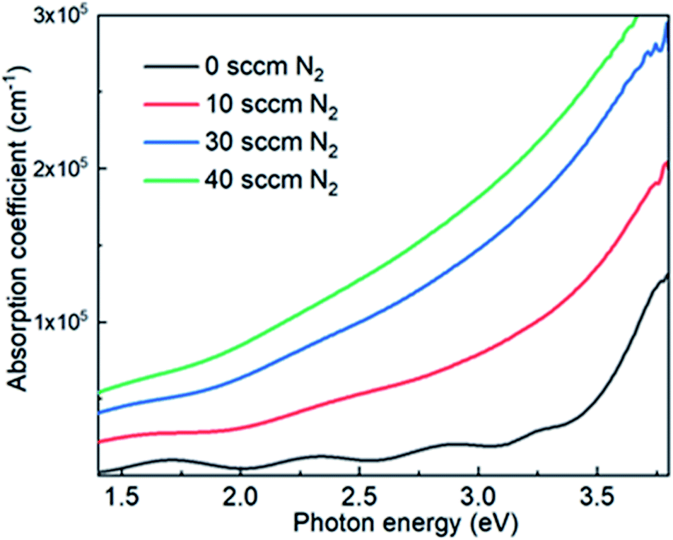 | ||
| Fig. 2 Optical absorption coefficients of N-doped NiO thin films grown with various N2 flow rates (0, 10, 30 and 40 sccm). | ||
The electrical properties of N-doped NiO thin films at room temperature as a function of the N2 flow rate are plotted in Fig. 3. It demonstrates that the nitrogen incorporation can tune the electrical properties significantly. Taking the resistivity as an example, it is reduced from 69![[thin space (1/6-em)]](https://www.rsc.org/images/entities/char_2009.gif) 200 (0 sccm N2) to 2268 (10 sccm N2), 273 (30 sccm N2) and 110 Ω cm (40 sccm N2). The mobility and carrier concentration have also been checked by AC Hall effect measurement. However, these two parameters of the undoped NiO (0 sccm N2) thin film could not be precisely determined probably due to its quite high resistivity indicating a probable low carrier concentration. In the case of other N-doped thin films (10, 30 and 40 sccm N2), the positive Hall coefficients imply the p-type conduction. As seen in Fig. 3, as increasing the N2 flow rate from 10 to 40 sccm, the mobility decreases from 3.4 to 0.14 cm2 V−1 s−1. On the contrary, the hole concentration rises up from 8.1 × 10¹⁴ to 4.0 × 1017 cm−3, indicating that nitrogen doping can increase the hole concentration remarkably. Since the increase of the hole concentration is higher than the mobility decrease, the addition of nitrogen induces a decrease of the film resistivity.
200 (0 sccm N2) to 2268 (10 sccm N2), 273 (30 sccm N2) and 110 Ω cm (40 sccm N2). The mobility and carrier concentration have also been checked by AC Hall effect measurement. However, these two parameters of the undoped NiO (0 sccm N2) thin film could not be precisely determined probably due to its quite high resistivity indicating a probable low carrier concentration. In the case of other N-doped thin films (10, 30 and 40 sccm N2), the positive Hall coefficients imply the p-type conduction. As seen in Fig. 3, as increasing the N2 flow rate from 10 to 40 sccm, the mobility decreases from 3.4 to 0.14 cm2 V−1 s−1. On the contrary, the hole concentration rises up from 8.1 × 10¹⁴ to 4.0 × 1017 cm−3, indicating that nitrogen doping can increase the hole concentration remarkably. Since the increase of the hole concentration is higher than the mobility decrease, the addition of nitrogen induces a decrease of the film resistivity.
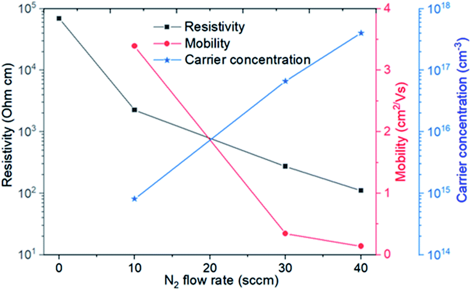 | ||
| Fig. 3 Resistivity, mobility and carrier concentration of N-doped NiO thin films as a function of N2 flow rate. | ||
To reveal the mechanism behind such tunable optical and electrical properties by nitrogen incorporation, the nitrogen chemical states have been investigated by EELS, which is a useful technique to acquire the fruitful information of materials, such as chemical states, optical constants and density of electronic states.34–36 The combination of EELS with TEM allows the penetration depth of several tens to hundred nanometers (depending on the acceleration voltage), rather than the surface sensitivity in traditional photoelectron spectroscopy (such as X-ray photoemission spectroscopy (XPS)), which may reduce the signal disturbance by surface effects and/or contamination. In addition, high spatial resolution of EELS embedded in TEM yields higher reliability on the physical origins of spectrum for deep analyses. For instance, the EELS spectra from the inside of grains and grain boundaries can be collected precisely for a comparison. The energy loss near edge structure (ELNES) spectrum of N–K edge of the N-doped NiO thin film (40 sccm N2) is shown in Fig. 4a. In addition, the N–K edge ELNES spectra of molecular N2,37 BN nanoparticles38 and AlN thin film are also plotted alongside for comparison. As seen, a sharp peak with the full width at half maximum (FWHM) of 1 eV located at near 400 eV is clearly identified in N-doped NiO thin film. Beside, another broad peak with small intensity is observed in the energy range of 405–430 eV. These spectral features look quite similar to those of molecular N2 (see Fig. 4a). On the contrary, the ELNES shows significant discrepancies with that of BN and AlN, where the spectra show multi-peak features with larger widths at the onset of the N–K edge. Therefore, these comparisons imply that the N–K edge ELNES spectrum of the N-doped thin film exhibits the N2 molecular state.
 | ||
| Fig. 4 (a) N–K edge ELNES spectra of N-doped NiO thin film, molecular N2,37 BN38 and AlN. All spectra are normalized to the peak height. (b) STEM image of N-doped NiO thin film grown with 40 sccm N2. The selected region for EELS line profile analyses is marked by a red line. (c) Heatmap of the ELNES intensity as a function of the position and energy loss. The number from 0 to 8 in y-axis corresponds to the position marked in (b) with an interval of around 1 nm. | ||
The nitrogen chemical states located inside the grains and at the grain boundaries have been studied by the EELS line profile. Scanning transmission electron microscopy (STEM) image of the N-doped NiO thin film grown with 40 sccm N2 is shown in Fig. 4b, where the red line indicates the selected region for EELS line profile analyses. Fig. 4c exhibits the heatmap of ELNES intensity as a function of the energy loss and position for nine measurement points with an interval of around 1 nm. As seen in Fig. 4c, the ELNES spectra show the sharp peaks at around 400 eV irrelevant to the positions. It indicates that the detected nitrogen always predominantly exhibits the molecular state in the N-doped thin film, regardless whether in grains or grain boundaries. Therefore, the molecular state of nitrogen seems to be the intrinsic properties in our samples. The nitrogen content in the N-doped NiO thin film (40 sccm N2) has been estimated by energy-dispersive spectroscopy (EDS) embedded in TEM, which gives the N composition of around 3.6 at%.
Fig. 5a shows formation energies of various N2-related defects. Several types of dimer N2 defects, including N2 on the nickel site (N2)Ni, N2 on the oxygen site (N2)O, N2 interstitial (N2)i, and N2 with multiple vacancies (N2 + VNi + VO, N2 + 2VNi + 2VO, and N2 + 4VNi + 4VO), have been taken into consideration. One can see that (N2)i shows very high formation energy, attributed to the huge size mismatch between the interstitial site and N2 molecule. Except for it, N2-related defects are relatively low in formation energies with deep levels. Especially, N2 + VNi + VO acts as deep acceptor with a relatively low formation energy. This is qualitatively consistent with our experimental results: (i) the subgap optical absorption increases significantly with increasing the N2 flow rate (see Fig. 2), and (ii) the hole mobility decreases with increasing the N2 flow rate (see Fig. 3).
 | ||
| Fig. 5 Formation energies of (a) dimer N2-related defects and (b) single N-related defects in NiO at the O-rich condition as a function of the Fermi level. Energy zero is set to the VBM. VaX means the vacancy of X element. Only the most energetically favorable charge state at a given Fermi level is shown for each defect. | ||
As shown in Fig. 5b, we also checked single N-related defects, including nitrogen on the nickel site (NNi), nitrogen on the oxygen site (NO), and nitrogen interstitial (Ni). Noticeably, NO is an acceptor with a low formation energy and shallower acceptor level than N2-related defects, which implies that NO can also increase the hole concentration. However, as discussed before, our EELS analysis indicates that most of the nitrogen elements exist in the form of N2 molecules in the doped NiO thin film. This discrepancy would be because of the strong stability of N2 molecule which is the source of nitrogen in this study; the calculated binding energy of the N–N triple bond is 10.4 eV, which is much higher than 6.75 eV of an O2 molecule. Therefore, the smaller concentration of the N anions is probable because the metastable N2-related states would become dominant in the non-equilibrium growth conditions. Indeed, the measured hole concentration is much lower than the contained nitrogen concentration.
In summary, a joint experimental and theoretical study is performed to investigate the influence of nitrogen doping on the optical and electrical properties of the NiO thin films. It is demonstrated in experiments that nitrogen incorporation in NiO can enhance the sub-gap absorption significantly, and the hole concentration is increased while the mobility is reduced. The nitrogen chemical state is predominantly identified as the molecular state (N2) based on the ELNES. Based on the theoretical calculations, the dimer N2-related defects would exist with coupling with multiple vacancies such as N2 + VNi + VO and hold deep acceptor levels. Furthermore, the increase of the hole concentration may be due to the introduction of nitrogen anions on the oxygen sites as they act as acceptors with relatively shallower acceptor levels in NiO.
Author contributions
Y. W. carried out main parts of the experiments and wrote the first version of this paper. Y. W. and J. F. P. proposed the concept. S. B. and J. G. performed TEM analyses. Y. K., N. T. and F. O. completed the theoretical calculations. H. S. and B. D. contributed to the analysis and discussion for the results. All authors commented on the manuscript.Conflicts of interest
There are no conflicts to declare.Acknowledgements
This work is supported by the National Science Foundation of China (51702267), the Open Project of State Key Laboratory of Environment-friendly Energy Materials (19kfhg14) and the Qilu Young Scholar at Shandong University. The Centre de Compétences X-Gamma of the Institut Jean Lamour is acknowledged for his technical support.References
- H. Ohta, M. Hirano, K. Nakahara, H. Maruta, T. Tanabe, M. Kamiya, T. Kamiya and H. Hosono, Fabrication and photoresponse of a pn-heterojunction diode composed of transparent oxide semiconductors, p-NiOand n-ZnO, Appl. Phys. Lett., 2003, 83, 1029 CrossRef CAS.
- M. Patel, H. S. Kim and J. Kim, All Transparent Metal Oxide Ultraviolet Photodetector, Adv. Electron. Mater., 2015, 1, 1500232 CrossRef.
- M. Patel, H. S. Kim, J. Kim, J. H. Yun, S. J. Kim, E. H. Choi and H. H. Park, Excitonic metal oxide heterojunction (NiO/ZnO) solar cells for all-transparent module integration, Sol. Energy Mater. Sol. Cells, 2017, 170, 246 CrossRef CAS.
- Y. B. Wang, X. H. Wei, L. Chang, D. G. Xu, B. Dai, J. F. Pierson and Y. Wang, Room temperature fabrication of transparent p-NiO/n-ZnO junctions with tunable electrical properties, Vacuum, 2018, 149, 331 CrossRef CAS.
- J. Jeng, K. Chen, T. Chiang, P. Lin, T. Tsai, Y. Chang, T. Guo, P. Chen, T. Wen and Y. Hsu, Nickel Oxide Electrode Interlayer in CH3NH3PbI3 Perovskite/PCBM Planar-Heterojunction Hybrid Solar Cells, Adv. Mater., 2014, 26, 4107 CrossRef CAS PubMed.
- C. Hu, Y. Bai, S. Xiao, K. Tao, W. Kit Ng, K. Sing Wong, S. Hang Cheung, S. Kong So, Q. Chen and S. Yang, Surface Sulfuration of NiO Boosts the Performance of Inverted Perovskite Solar Cells, Sol. RRL, 2020, 4, 2000270 CrossRef CAS.
- P. Gupta, T. Dutta, S. Mal and J. Narayan, Controlled p-type to n-type conductivity transformation in NiO thin films by ultraviolet-laser irradiation, J. Appl. Phys., 2012, 111, 013706 CrossRef.
- J. Y. Zhang, W. W. Li, R. L. Z. Hoye, J. L. Macmanus-Driscoll, M. Budde, O. Bierwagen, L. Wang, Y. Du, M. J. Wahila, L. F. J. Piper, T. L. Lee, H. J. Edwards, V. R. Dhanak and K. H. L. Zhang, Electronic and transport properties of Li-doped NiO epitaxial thin films, J. Mater. Chem. C, 2018, 6, 2275 RSC.
- D. Das, M. Pal, E. Di Bartolomeo, E. Traversa and D. Chakravorty, Synthesis of nanocrystalline nickel oxide by controlled oxidation of nickel nanoparticles and their humidity sensing properties, J. Appl. Phys., 2000, 88, 6856 CrossRef CAS.
- R. Asahi, T. Morikawa, T. Ohwaki, K. Aoki and Y. Taga, Visible-light photocatalysis in nitrogen-doped titanium oxides, Science, 2001, 293, 269 CrossRef CAS PubMed.
- T. Yoshida, S. Niimi, M. Yamamoto, T. Nomoto and S. Yagi, Effective nitrogen doping into TiO2 (N-TiO2) for visible light response photocatalysis, J. Colloid Interface Sci., 2014, 447, 278 CrossRef PubMed.
- C. Burda, Y. Lou, X. Chen, A. C. S. Samia, J. Stout and J. L. Gole, Enhanced Nitrogen Doping in TiO2 Nanoparticles, Nano Lett., 2003, 3, 1049 CrossRef CAS.
- A. Panepinto, D. Cornil, P. Guttmann, C. Bittencourt, J. Cornil and R. Snyders, Fine Control of the Chemistry of Nitrogen Doping in TiO2: A Joint Experimental and Theoretical Study, J. Phys. Chem. C, 2020, 124, 17401 CrossRef CAS.
- J. T-Thienprasert and S. Limpijumnong, Identification of nitrogen acceptor in Cu2O: First-principles study, Appl. Phys. Lett., 2015, 107, 221905 CrossRef.
- Y. Wang, J. Ghanbaja, D. Horwat, L. Yu and J. F. Pierson, Nitrogen chemical state in N-doped Cu2O thin films, Appl. Phys. Lett., 2017, 110, 131902 CrossRef.
- Y. S. Lee, J. Heo, M. T. Winkler, S. C. Siah, S. B. Kim, R. G. Gordon and T. Buonassisi, Nitrogen-doped cuprous oxide as a p-type hole-transporting layer in thin-film solar cells, J. Mater. Chem. A, 2013, 1, 15416 RSC.
- Z. Zhao, X. He, J. Yi, C. Ma, Y. Cao and J. Qiu, First-principles study on the doping effects of nitrogen on the electronic structure and optical properties of Cu2O, RSC Adv., 2013, 3, 84 RSC.
- M. Nolan, R. Long, N. J. English, D. A. Mooney, M. Nolan, R. Long, N. J. English and D. A. Mooney, Hybrid density functional theory description of N-and C-doping of NiO, J. Chem. Phys., 2011, 134, 224703 CrossRef PubMed.
- J. Keraudy, A. Ferrec, M. Richard-Plouet, J. Hamon, A. Goullet and P. Y. Jouan, Nitrogen doping on NiO by reactive magnetron sputtering: a new pathway to dynamically tune the optical and electrical properties, Appl. Surf. Sci., 2017, 409, 77 CrossRef CAS.
- P. E. Blochl, Projector augmented-wave method, Phys. Rev. B: Condens. Matter Mater. Phys., 1994, 50, 17953 CrossRef PubMed.
- G. Kresse and J. Furthmu, Efficient iterative schemes for ab initio total-energy calculations using a plane-wave basis set, Phys. Rev. B: Condens. Matter Mater. Phys., 1996, 54, 11169 CrossRef CAS PubMed.
- G. Kresse and D. Joubert, From ultrasoft pseudopotentials to the projector augmented-wave method, Phys. Rev. B: Condens. Matter Mater. Phys., 1999, 59, 1758 CrossRef CAS.
- R. Long, N. J. English and D. A. Mooney, Electronic structures of N-and C-doped NiO from first-principles calculations, Phys. Lett. A, 2010, 374, 1184 CrossRef CAS.
- S. L. Dudarev, G. A. Botton, S. Y. Savrasov, C. J. Humphreys and A. P. Sutton, Electron-energy-loss spectra and the structural stability of nickel oxide: An LSDA+U study, Phys. Rev. B: Condens. Matter Mater. Phys., 1998, 57, 1505 CrossRef CAS.
- Y. Kumagai and F. Oba, Electrostatics-based finite-size corrections for first-principles point defect calculations, Phys. Rev. B: Condens. Matter Mater. Phys., 2014, 89, 195205 CrossRef.
- A. Mallikarjuna Reddy, A. Sivasankar Reddy, K.-S. Lee and P. Sreedhara Reddy, Growth and characterization of NiO thin films prepared by dc reactive magnetron sputtering, Solid State Sci., 2011, 13, 312–320 Search PubMed.
- X. Chen and C. Burda, The Electronic Origin of the Visible-Light Absorption Properties of C-, N- and S-Doped TiO2 Nanomaterials, J. Am. Chem. Soc., 2008, 130, 5018 CrossRef CAS PubMed.
- H. Sun, S. C. Chen, S. W. Hsu, C. K. Wen, T. H. Chuang and X. Wang, Microstructures and optoelectronic properties of nickel oxide films deposited by reactive magnetron sputtering at various working pressures of pure oxygen environment, Ceram. Int., 2017, 43, S369 CrossRef CAS.
- K. S. Usha, R. Sivakumar and C. Sanjeeviraja, Optical constants and dispersion energy parameters of NiO thin films prepared by radio frequency magnetron sputtering technique, J. Appl. Phys., 2013, 114, 123501 CrossRef.
- J. Keraudy, B. Delfour-Peyrethon, A. Ferrec, J. Garcia Molleja, M. Richard-Plouet, C. Payen, J. Hamon, B. Corraze, A. Goullet and P. Y. Jouan, Process- and optoelectronic-control of NiOx thin films deposited by reactive high power impulse magnetron sputtering, J. Appl. Phys., 2017, 121, 171916 CrossRef.
- C. Rödl, F. Fuchs, J. Furthmüller and F. Bechstedt, Quasiparticle band structures of the antiferromagnetic transition-metal oxides MnO, FeO, CoO, and NiO, Phys. Rev. B: Condens. Matter Mater. Phys., 2009, 79, 235114 CrossRef.
- S. Lany, Semiconducting transition metal oxides, J. Phys.: Condens. Matter, 2015, 27, 283203 CrossRef PubMed.
- S. Lany, Band-structure calculations for the 3d transition metal oxides in GW, Phys. Rev. B: Condens. Matter Mater. Phys., 2013, 87, 085112 CrossRef.
- R. F. Egerton, Electron Energy-Loss Spectroscopy, Springer, 2011 Search PubMed.
- Y. Wang, J. Ghanbaja, S. Bruyère, P. Boulet, F. Soldera, D. Horwat, F. Mücklich and J. F. Pierson, Local heteroepitaxial growth to promote the selective growth orientation, crystallization and interband transition of sputtered NiO thin films, CrystEngComm, 2016, 18, 1732 RSC.
- Y. Wang, S. Lany, J. Ghanbaja, Y. Fagot-Revurat, Y. P. Chen, F. Soldera, D. Horwat, F. Mücklich and J. F. Pierson, Electronic structures of Cu2O, Cu4O3 and CuO: A joint experimental and theoretical study, Phys. Rev. B: Condens. Matter Mater. Phys., 2016, 94, 245418 CrossRef.
- M. Terrones, R. Kamalakaran, T. Seeger and M. Ruhle, Novel nanoscale gas containers: encapsulation of N2 in CNx nanotubes, Chem. Commun., 2000, 23, 35 Search PubMed.
- A. N. Fioretti, C. P. Schwartz, J. Vinson, D. Nordlund, D. Prendergast, A. C. Tamboli, C. M. Caskey, F. Tuomisto, F. Linez, S. T. Christensen, E. S. Toberer, S. Lany and A. Zakutayev, Understanding and control of bipolar self-doping in copper nitride, J. Appl. Phys., 2016, 119, 181508 CrossRef PubMed.
| This journal is © The Royal Society of Chemistry 2022 |