
 Open Access Article
 This Open Access Article is licensed under a Creative Commons Attribution-Non Commercial 3.0 Unported Licence
High efficiency and low operating voltage yellow phosphorescent organic light-emitting diodes with a simple doping-free structure
Jie Hua *ab,
Jiaxin Liab,
Zhuolin Zhanb,
Yuan Chaiab,
Zeyuan Chengb,
Peiding Lib,
He Dongab and
Jin Wangab
*ab,
Jiaxin Liab,
Zhuolin Zhanb,
Yuan Chaiab,
Zeyuan Chengb,
Peiding Lib,
He Dongab and
Jin Wangab
aKey Laboratory of Functional Materials Physics and Chemistry of the Ministry of Education, Jilin Normal University, Siping 136000, China. E-mail: huajie@jlnu.edu.cn
bCollege of Information Technology, Jilin Normal University, Siping 136000, China
First published on 9th August 2022
Abstract
Yellow phosphorescent organic light-emitting diodes (PhOLEDs) with high efficiency and a low operating voltage were reported through using a simple doping-free structure. The structure of the PhOLEDs was ITO/C60/MoO3/mCP/PO-01-TB/PO-T2T/Liq/Al. The np-type C60/MoO3 heterojunction acted as hole injection layer, and the ultrathin PO-01-TB layer (0.1 nm) was inserted at the interface between mCP and PO-T2T to serve as yellow phosphorescent emitter. Detailed investigation suggested that the complete energy transfer occurred from the mCP/PO-T2T interfacial exciplex to yellow PO-01-TB. Furthermore, the np-type C60/MoO3 heterojunction could supply more free charge carriers, giving rise to further enhanced PhOLED efficiency. By adjusting the thickness of the C60/MoO3 heterojunction, a yellow PhOLED with a power efficiency of 71.6 lm W−1 was demonstrated with an extremely low operating voltage of 3.79 V at 1000 cd m−2.
1. Introduction
Much endeavor has been made to pursue high performance organic light-emitting diodes (OLEDs) in the past three decades because of their huge potential applications in solid state lighting and full color flat panel displays.1–4 According to the different types of emitting materials used in devices, OLEDs are divided into fluorescent OLEDs (FlOLEDs) and phosphorescent OLEDs (PhOLEDs). As compared with traditional fluorescent emitters, phosphorescent emitters can harvest both singlet S1 and triplet T1 excitons for electroluminescence (EL) owing to the heavy-atom effect, so that they can realize 100% internal quantum efficiency (IQE), showing a great potential for developing high-performance OLEDs.5–8 To avoid the concentration quenching effects between phosphorescent molecules induced by strong intermolecular interaction, a host-guest doping system is normally adopted in PhOLEDs. This means that choosing a proper host for a phosphorescent emitter is a key strategy to achieve high efficiency PhOLEDs.Traditional PhOLEDs usually use hole transport materials as host matrix. Unfortunately, this type host can render unbalance charge transport,9 thus worsening the exciton quenching effects.8,10 To address those issues, PhOLEDs utilizing neutral exciplex as co-host have attracted more attentions recently. The exciplex is formed through the charge transfer between electron transporting material (electron donor) and hole transporting material (electron acceptor), showing obvious bipolar charge transport as well as high triplet energy, which reducing the polaron accumulation to restrain exciton quenching. Moreover, owing to small orbital overlap between the excited state and the ground state, most exciplex possess a small ΔEst (S1–T1 energy splitting), which promotes the energy transfer process changing from Dexter energy transfer to Förster energy transfer in host-guest doping system.8,11–17 For example, Park et al.16 doped bis(2-phenylpyridine)(acetylacetonato) iridium(III) (Ir(ppy)2acac) into the exciplex co-host formed by 4,4′,4′′-tri(N-carbazolyl)triphenylamine(TCTA) and bis-4,6-(3,5-di-3-pyridylphenyl)-2-methylpyrimidine (B3PYMPM) to achieve green PhOLED with low turn-on voltage of 2.4 V and high external quantum efficiency (EQE) of 29.1% as well as low roll-off. Wang et al.17 employed interfacial exciplex of (N,N′-di(naphth-1-yl)-N,N′-diphenyl-benzidine (NPB)/1,3,5 tris[N-(phenyl)benzimidazole]-benzene (TPBi) as co-host to fabricate a red PhOLED showing a high EQE of 17.2% and a low turn-on voltage of 2.6 V simultaneously. These results suggest that the exciplex with unique photophysical properties become a potential alternative for developing high performance PhOLEDs.
For the PhOLEDs, the efficient charge injection is another key factor for achieving high performance. For hole injection, P-type transition metal oxides-molybdenum trioxide (MoO3) with high transparency and work function shows strong hole injection ability, and has been widely used as hole injection layer (HIL) to reduce the injection barriers of hole from anode ITO and attain transport balance of the charge carriers.18–20 As for as n-type C60 semiconductor, owing to its significant exciton dissociation behavior, it has been used as electron acceptor in photogalvanic cells,21 while in OLEDs it acts as modifier for electrodes to enhance hole injection.22–24 Recently organic heterojunction consisting of n-type C60 and p-type pentacene (or CuPc), exhibits excellent charge generation effect and is used as charge generation layers (GGLs) in tandem OLEDs to improved power efficiency.25,26 Based on the charge generation effect, Chen et al.27 utilized C60/pentacene heterojunction as HIL to achieve highly efficient OLEDs. This discovery allows the np-type heterojunction to explore novel HIL architecture in OLEDs.
In this work, we reported a yellow PhOLED with high performance through employing np-type C60/MoO3 heterojunction as HIL and interfacial exciplex as co-host system. The interfacial exciplex was formed at the interface between 1,3-bis(9H-carbazol-9-yl)benzene (mCP) and (1,3,5-triazine-2,4,6-triyl)tris(benzene-3,1-diyl))tris(diphenylphosphine oxide (PO-T2T). An ultrathin layer of Iridium(III)bis(4-(4-tert-butylphenyl)thieno[3,2-c]pyridinato-N,C2′) acetylacetonate (PO-01-TB) was inserted at the mCP and PO-T2T interface to serve as yellow phosphorescent emitter. The resulting yellow PhOLED exhibited high current efficiency (CE) of 56.7 cd A−1, power efficiency (PE) of 71.6 lm W−1, and EQE of 17.5%, as well as an extremely low operating voltage of 3.79 V at 1000 cd m−2. The achievement of such high performance was mainly attributed to the highly efficient carrier injection based on the np-type hole injector and efficient energy transfer between interfacial exciplex based on the interfacial exciplex co-host and phosphorescent guest.
2. Experimental details
All OLEDs were fabricated on clean glass substrates pre-coated indium tin oxide (ITO) with a sheet resistance of 15 Ω per square. Before evaporation, ITO substrates were cleaned sequentially with acetone, alcohol, and deionized water by scrubbing and sonication, and then dried at 130 °C and treated in an ultraviolet-ozone for 15 min before it was loaded into a deposition chamber. All layers were grown on ITO substrate in succession by conventional thermal deposition with the rates of ∼0.1 nm s−1 at high vacuum condition (∼4.0 × 10⁻⁴ Pa). After the deposition of an Al cathode with a rate of >0.1 nm s−1, the devices were completed. All the thicknesses and deposition rates for each layer were monitored in situ quartz crystal monitors. The active emission area was determined as 4 mm2 by the overlap between Al cathode and ITO anode. The photoluminescence (PL) spectra and transient PL decay curves were collected by a Horiba JobinYvon Fluorolog-3 spectrometer with a time-correlated single-photon counting (TCSPC) spectrometer. The current density–voltage–luminance characteristics of all devices were recorded by Keithley 2400 constant current source and SpectraScan PR-655 spectrometer. The CE, PE, and EQE of the OLEDs were calculated from the current density, luminance, and EL spectrum, assuming a Lambertian distribution. All measurements were formed at ambient atmosphere conditions.3. Results and discussion
3.1 The formation of exciplex between mCP and PO-T2T
To demonstrate the formation of exciplex between mCP and PO-T2T, we firstly fabricated mCP (20 nm), PO-T2T (20 nm) pure films and mCP:PO-T2T (molar ratio of 1![[thin space (1/6-em)]](https://www.rsc.org/images/entities/char_2009.gif) :1, 20 nm) doping film, and measured their PL spectra under excitation wavelength of 325 nm as shown in Fig. 1(a). The PL peak of mCP film is located at 375 nm companying with shoulder peak at 395 nm. The PO-T2T film exhibits strong emission peak at 384 nm and a weak board emission band at 534 nm. The weak peak is assigned to excimer emission. Compared to the pure mCP and PO-T2T films, a broad emission at 472 nm can be observed in mCP:PO-T2T doping film. Fig. 1(b) depicts the energy level diagram to show the exciplex formation process between mCP and PO-T2T. The emission peak energy 2.63 eV (472 nm) of the mCP:PO-T2T doping film is nearly closed to the energy offset 2.6 eV between the lowest unoccupied molecular orbital (LUMO) level of PO-T2T (3.5 eV) and the highest occupied molecular orbital (HOMO) level of mCP (6.1 eV), suggesting that the broad emission band arises from the mCP:PO-T2T-forming exciplex. In addition, we measured the EL spectra of mCP/PO-T2T and mCP:PO-T2T as shown in Fig. 1(a). The exciplex can also be formed at the mCP/PO-T2T interface. Compared the mCP/PO-T2T double films with mCP:PO-T2T doping film, no obvious change in their EL spectra are observed. In addition, the EL spectrum of the exciplex is almost the same as its PL spectrum.
:1, 20 nm) doping film, and measured their PL spectra under excitation wavelength of 325 nm as shown in Fig. 1(a). The PL peak of mCP film is located at 375 nm companying with shoulder peak at 395 nm. The PO-T2T film exhibits strong emission peak at 384 nm and a weak board emission band at 534 nm. The weak peak is assigned to excimer emission. Compared to the pure mCP and PO-T2T films, a broad emission at 472 nm can be observed in mCP:PO-T2T doping film. Fig. 1(b) depicts the energy level diagram to show the exciplex formation process between mCP and PO-T2T. The emission peak energy 2.63 eV (472 nm) of the mCP:PO-T2T doping film is nearly closed to the energy offset 2.6 eV between the lowest unoccupied molecular orbital (LUMO) level of PO-T2T (3.5 eV) and the highest occupied molecular orbital (HOMO) level of mCP (6.1 eV), suggesting that the broad emission band arises from the mCP:PO-T2T-forming exciplex. In addition, we measured the EL spectra of mCP/PO-T2T and mCP:PO-T2T as shown in Fig. 1(a). The exciplex can also be formed at the mCP/PO-T2T interface. Compared the mCP/PO-T2T double films with mCP:PO-T2T doping film, no obvious change in their EL spectra are observed. In addition, the EL spectrum of the exciplex is almost the same as its PL spectrum.
 | ||
| Fig. 1 (a) Photoluminescence (PL) spectra of mCP and PO-T2T pure films, and mCP:PO-T2T doping film on crystal substrates with excitation wavelength of 325 nm. (b) Energy level diagram showing the exciplex formation process between mCP and PO-T2T interface. | ||
3.2 Exciton distribution in mCP/PO-T2T co-host system
In order to simplify the fabrication process, the double layer structure mCP/PO-T2T was used to replace the doping structure mCP:PO-T2T to fabricated PhOLEDs. Firstly, we fabricated PhOLEDs by introducing yellow phosphor PO-01-TB to elucidate the exciton distribution in mCP/PO-T2T system. The structure of device A1 is illustrated as follows: ITO/mCP(60 nm)/PO-T2T(10 nm)/PO-01-TB(0.1 nm)/PO-T2T(30 nm)/Liq(2 nm)/Al, and the architecture of other devices is ITO/mCP (60−x nm)/PO-01-TB(0.1 nm)/mCP(x nm)/PO-T2T(40 nm)/Liq(2 nm)/Al, where x = 0, 10, 20, and 30 nm corresponding to the device A2, A3, A4, and A5, respectively. Here, the emitting layer PO-01-TB is so extremely thin (0.1 nm) that it would insignificantly affect the electrical properties of the resulting device.Fig. 2(a) shows the normalized EL spectra of the devices A1–A5 at a current density of 20 mA cm−2. It can be observed that the emission peak of devices A1–A5 shows significant difference. In detail, as PO-01-TB is employed into PO-T2T layer (device A1), the EL spectrum exhibits two emission peaks. The strong emission at 472 nm should originate from the mCP/PO-T2T-forming interfacial exciplex, while the weak emission at 560 nm can be attributed to PO-01-TB. Fig. 2(b) presents the schematic diagram and the energy levels of the devices A1–A5 with different position of ultrathin PO-01-TB layer. Owing to the large energy barrier for electrons (1.1 eV) and holes (1.4 eV) at the mCP/PO-T2T interface, it is difficult for carriers to cross over the interface. Hence, most holes and electrons should accumulate at the mCP/PO-T2T interface area and generate the interfacial exciplex. Weak emission from PO-01-TB reveals a few exciton can form in the PO-T2T layer. When the PO-01-TB layer is located at the interface of mCP/PO-T2T (device A2), the EL spectrum only shows pure yellow emission at 560 nm with subpeak at 596 nm from PO-01-TB, while the peak of the exciplex is disappear.
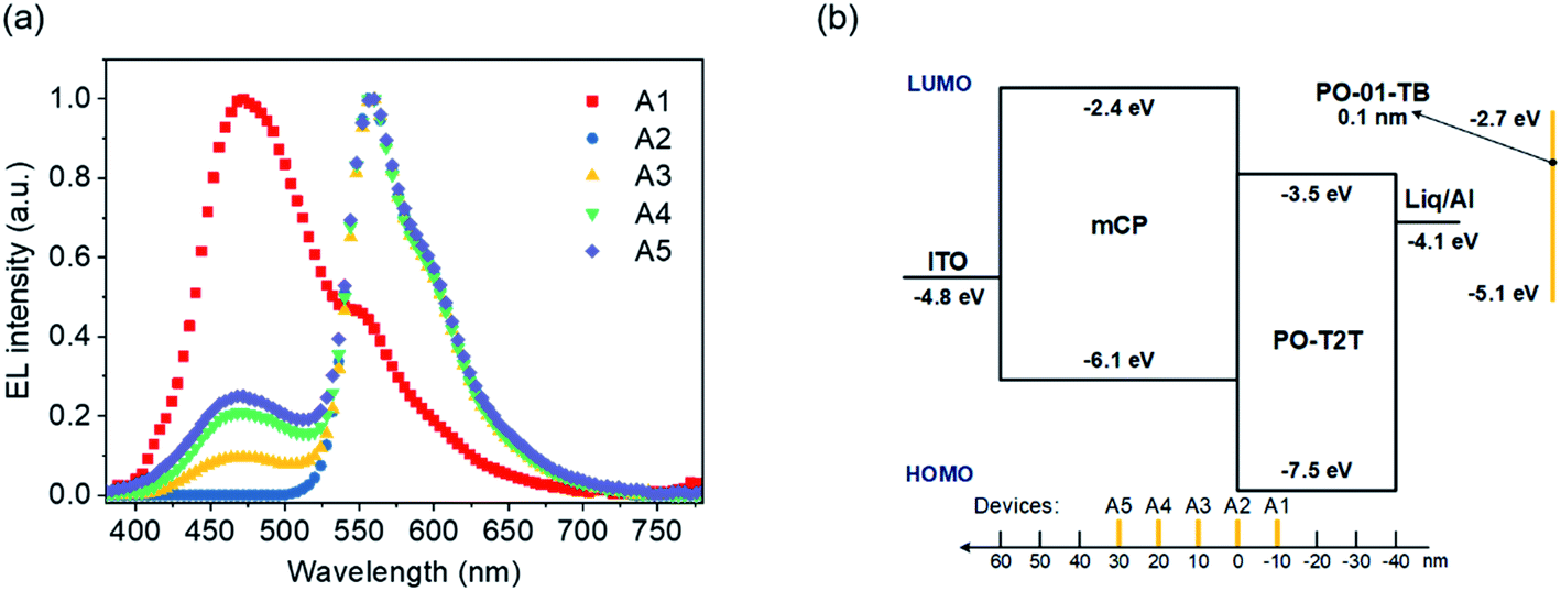 | ||
| Fig. 2 (a) EL spectra of the devices A1–A5 at 20 mA cm−2. (b) The structures of the devices A1–A5 and the detailed energy level diagram of the materials. The bottom gives the distance of PO-01-TB to the interface of mCP/PO-T2T in devices A1–A5. | ||
Fig. 3 presents the transient PL (TRPL) decay behavior at room temperature for the PO-T2T/mCP and PO-T2T/PO-01-TB/mCP films. Typical two lifetimes of prompt and delayed are observed under 472 nm with mCP/PO-T2T-forming interfacial exciplex. The TRPL signal was fitted by a double-exponential decaying function. The prompt and delayed lifetime of the PO-T2T/mCP film were measured to be longer than that of the PO-T2T/PO-01-TB/mCP film, which is presumably due to the energy transfer process from mCP/PO-T2T-forming interfacial exciplex to PO-01-TB. Considering the T1 energy level (T1 = 2.69 eV) of the mCP/PO-T2T-forming interfacial exciplex28 higher than that of PO-01-TB (T1 = 2.20 eV), and lower than that of mCP (2.90 eV) and PO-T2T (2.99 eV), the efficient energy transfer process can be occurred from the mCP/PO-T2T-forming interfacial exciplex to PO-01-TB emitter, resulting in yellow phosphorescent emission.29–31 As for as the devices A3–A5, the ultrathin PO-01-TB layer is inserted into mCP layer (i.e. x = 10, 20, 30) away from the interface of mCP/PO-T2T, two emission peaks from the exciplex (472 nm) and PO-01-TB (560 nm) appears simultaneously. Because of its shallower HOMO levels than that of mCP, PO-01-TB can act as a hole trap for carriers when doped in mCP and recombine at the PO-01-TB layer. With increasing the values of x, the decreasing hole carrier concentration results in the decrease in the relative emission intensity from PO-01-TB.
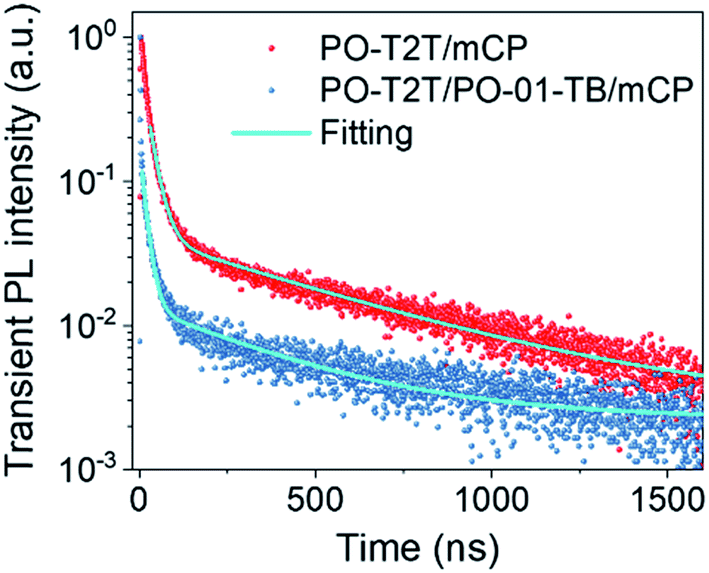 | ||
| Fig. 3 The transient PL decayed curves of the PO-T2T/mCP and PO-T2T/PO-01-TB/mCP films at 300 K. | ||
3.3 PhOLED based on np-type C60/MoO3 composited HIL
According to the discussion above, inserting the ultrathin PO-01-TB layer in mCP/PO-T2T interface can benefit to realize pure yellow emission through complete energy transfer. In order to achieve high efficiency of PO-01-TB based PhOLEDs, we proposed to employ np-type C60/MoO3 heterojunction as HIL and interfacial exciplex as host. The device configuration is as follows: ITO/HIL/mCP(60 nm)/PO-01-TB(0.1 nm)/PO-T2T (40 nm)/Liq(2 nm)/Al. For a conventional device HIL is MoO3(5 nm) (device B1). For np-type devices, HIL is C60(1 nm)/MoO3(y nm), where y = 4, 3, 2, and 1 nm corresponding to devices B2, B3, B4, and B5, respectively. Fig. 4 shows the energy diagram and the normalized EL spectra of the devices B1–B5. The five devices exhibit almost same EL spectra with the emission peak at 560 nm from PO-01-TB, indicating that the change in HIL structure could not affect the emission property of the devices. | ||
| Fig. 4 (a) Structure and the energy diagram and (b) EL spectra of the devices B1–B5. | ||
From Fig. 5(a), the current density of the devices B2–B5 fabricated utilizing a np-type C60/MoO3 HIL is higher than that of the device B1 fabricated with a MoO3 HIL at the same operating voltage. This could be attributed to enhancement of hole injection ability of np-type C60/MoO3 HIL. The main EL performances of all devices are summarized in Table 1. The turn-on voltage (at 1 cd m−2) of the device B1 and the devices B2–B5 are 2.70 V and about 2.46–2.55 V. The rather low turn-on voltage of 2.46 V for device B3 is very close to the thermodynamic limit, indicating that almost no potential barrier for hole injection is presented due to the introduction of C60 layer. In addition, the voltage of the devices B2–B5 decrease significantly compared with the device B1 at the same luminance as shown in Fig. 5(b). The operating voltages (at 1000 cd m−2) of devices B1, B2, B3, B4, and B5 are 5.92, 5.24, 3.99, 4.13, and 4.05 V, respectively. The operating voltage of the device B3 is reduced by 32.6% compared to that of device B1. Therefore, compared with the device B1, the current density and luminance of device B2–B5 with C60/MoO3 as HIL are obviously improved.
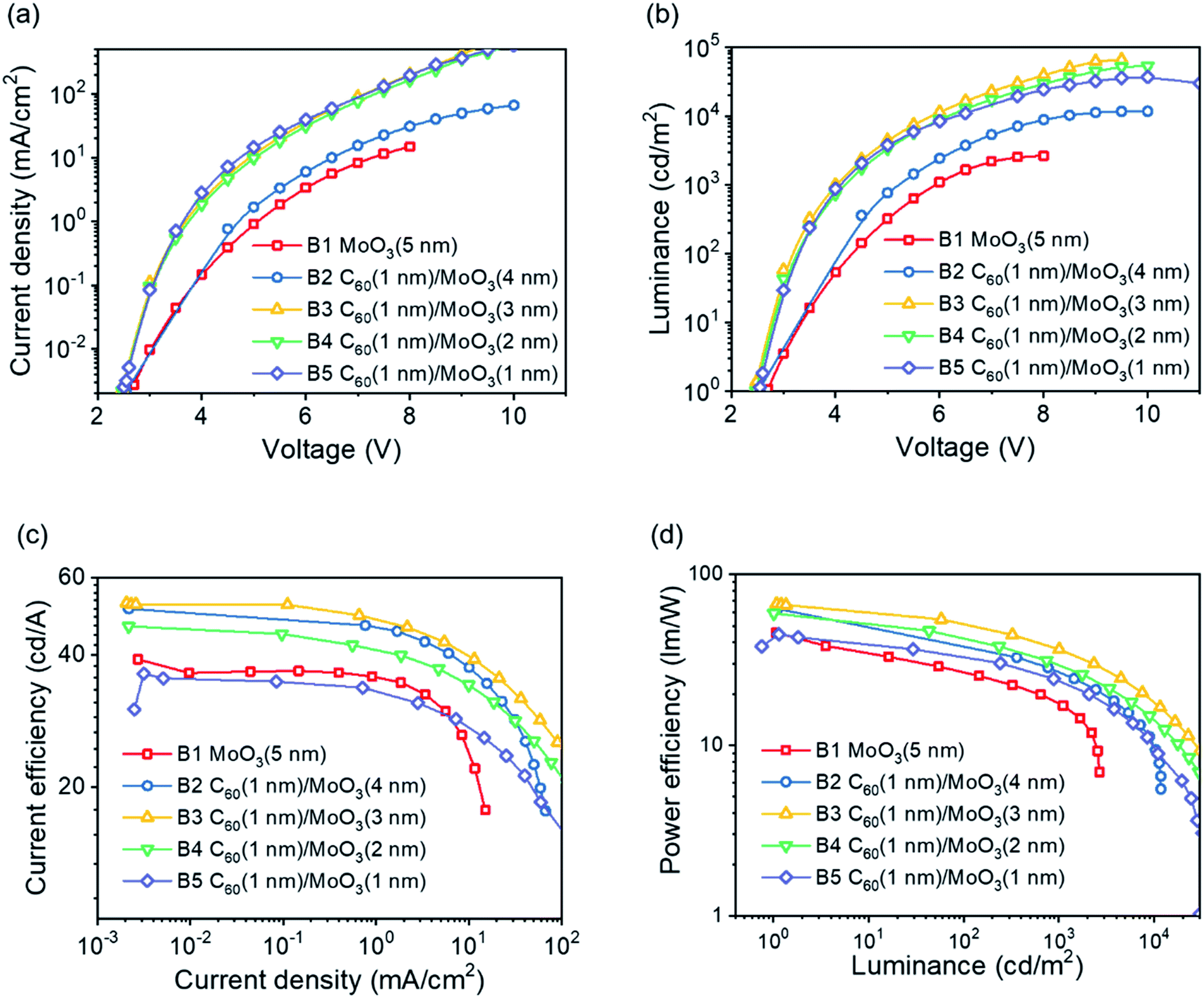 | ||
| Fig. 5 Comparison of the EL performances of devices B1–B5: (a) Current density–voltage (J–V) characteristics; (b) Luminance–voltage (L–V) characteristics; (c) Current efficiency–current density (CE–J) characteristics; (d) Power efficiency–luminance (PE–L) characteristics. | ||
| Device | Voltage (V) | Maximum | @1000 cd m−2 | @5000 cd m−2 |
|---|---|---|---|---|
| @1a/1000/5000 cd m−2 | EQEb/CEc/PEd (%/cd A−1/lm W−1) | |||
| a Turn-on voltage at a brightness of 1 cd m−2.b External quantum efficiency.c Current efficiency.d Power efficiency. | ||||
| B1 | 2.70/5.92/— | 12.5/39.1/45.5 | 10.0/32.8/17.4 | — |
| B2 | 2.55/5.24/6.85 | 16.4/51.0/62.9 | 13.4/44.0/26.9 | 10.6/35.3/16.1 |
| B3 | 2.46/3.99/5.06 | 16.5/52.6/67.2 | 13.7/46.4/36.4 | 11.4/38.8/24.1 |
| B4 | 2.47/4.13/5.33 | 14.4/47.5/59.2 | 11.6/39.3/30.0 | 9.5/32.2/19.1 |
| B5 | 2.53/4.05/5.28 | 11.5/36.3/44.7 | 9.0/34.1/24.0 | 7.2/24.6/14.7 |
| C1 | 2.48/4.24/5.41 | 14.2/47.9/55.2 | 12.7/43.1/31.4 | 10.5/34.9/20.7 |
| C2 | 2.43/3.86/4.76 | 17.5/56.8/71.6 | 15.1/52.1/41.5 | 12.7/43.6/29.1 |
| C3 | 2.51/4.59/5.92 | 16.0/51.1/62.4 | 14.3/48.3/32.1 | 11.7/38.4/20.9 |
Considering the low hole mobility (2.8 × 10⁻⁷ cm2 Vs−1)32 and high HOMO energy level (6.2 eV),33 the C60 layer may block parts of the holes injection from the anode ITO to MoO3 in the devices B2–B5, and one can predict that the current density should decreases and the turn-on voltage increases. However, in our work, the C60-containing devices B2–B5 show lower turn-on voltage and higher current density than the device B1. This means that the hole injection efficiency is significant enhanced due to the introduction of np-type C60/MoO3 HIL, which is consistent with the reported results for C60/pentacene as the hole injector in ref. 27. According to the “p–n junction” characteristic of C60/MoO3 heterojunction, free carriers can be effectively generated at the C60/MoO3 interface. Then, under the applied electrical field, the generated electrons can be extracted from LUMO of C60 to the ITO, while the generated holes are easily injected from HOMO of MoO3 into mCP, and combine with the electrons injected from the cathode to form the exciplex at mCP/PO-T2T interface. Subsequently the exciplex transfer its energy to PO-01-TB and then achieving yellow phosphorescent emission. From Fig. 5(c), (d) and Table 1, the device B3 exhibits a high CE, PE, and EQE of 52.6 cd A−1, 67.2 lm W−1, 16.5%, respectively, which are increased by approximately 34.5%, 47.7%, and 32% compared to that of the device B1 (only MoO3 as HIL). It is vital to point out that the efficiency-luminance roll-off of the device B3 is relatively mild with respect to the device B1. With the luminance rising to 1000 cd m−2 (2.16 mA cm−2), the CE, PE, and EQE could be kept at 46.4 cd A−1, 36.4 lm W−1, and 13.7%, respectively. Thus, the further enhanced EL performances of the device B3 should be ascribed to the increasing electric field on C60/MoO3 heterojunction due to the decreasing thickness of MoO3 film.
In order to deeply understand the hole transporting properties of np-type C60/MoO3 HIL, the hole-only single-carrier devices with structure of ITO/C60(1 nm), MoO3(5 nm), or C60(1 nm)/MoO3(3 nm)/mCP(60 nm)/PO-01-TB(0.1 nm)/PO-T2T(10 nm)/mCP(30 nm)/Al were fabricated. The J–V characteristics of these devices are displayed in Fig. 6. A comparison of the current density at the same operating voltage of the hole-only devices clearly indicates that the hole current in the np-type C60/MoO3 HIL device is higher than that in the C60 and MoO3 HIL devices, which can be attributed to the improved conductivity of the HIL with the np-type C60/MoO3. The results clearly demonstrate that the np-type C60/MoO3 heterojunction does be an effective hole injector to realize high performance OLEDs.
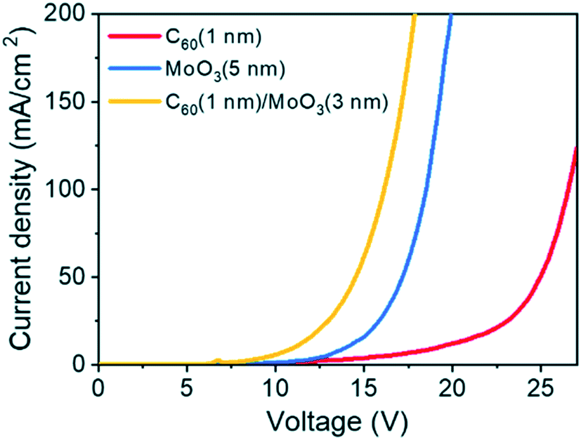 | ||
| Fig. 6 Current density–voltage (J–V) characteristics of hole-only devices. | ||
One key design of device B3 is the introduction of C60/MoO3 composite as HIL. To optimize the EL properties of device B3, the comparable devices were fabricated with structure of ITO/C60 (x nm)/MoO3(3 nm)/mCP(60 nm)/PO-01-TB(0.1 nm)/PO-T2T(40 nm)/Liq(2 nm)/Al, while x = 0.5, 2, 3 nm corresponds to devices C1–C3, respectively. Except of the thickness of C60 layer, other layers are kept the same as the device B3. Fig. 7 shows the J–V, L–V, CE–J, and PE–L characteristics of devices C1–C3 and B3, and the key performance parameters are summarized in Table 1. The resulting OLEDs performance in operating voltage and efficiency exhibits the dependence on the thickness of C60 layer. The current density first increases with the thickness x of C60 from 0.5 to 2 nm, and then it decreases as further increasing x to 3 nm. Moreover, at the luminance of 1000 cd m−2, the operating voltages are 4.24, 3.99, 3.86, and 4.59 V for the devices with x = 0.5, 1, 2, and 3 nm, respectively (shown in Fig. 7(b)). These results indicate that properly increasing the thickness of C60 is beneficial to the formation of excellent np-junction C60/MoO3 for the efficient charge generation and injection. However, the low hole mobility and high HOMO energy level of C60 will inferior for hole injection and transport,23 which results in low current density and high operating voltage in device C3 with 3 nm-C60 layer. The device C2 (x = 2 nm) shows the best performance with a maximum CE, PE, and EQE of 56.8 cd A−1, 71.6 lm W−1, and 17.5%, respectively. Notably, the CE still keep as high as 52.1% at 1000 cd m−2 (1.97 mA cm−2), showing extremely low efficiency roll-off of 8.3%.
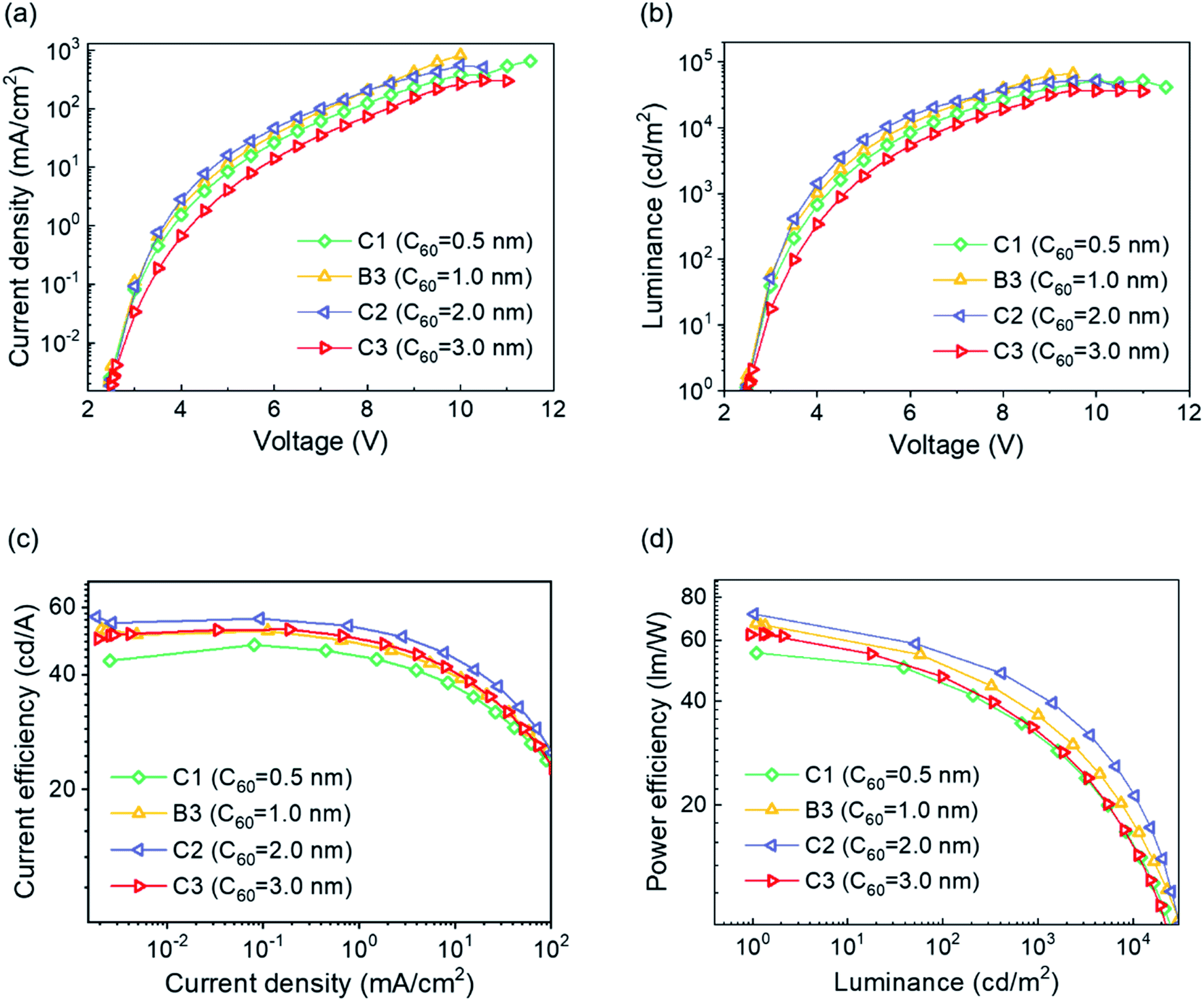 | ||
| Fig. 7 EL performances of devices C1–C3 and B3 with the different thickness of C60 layer. (a) Current density–voltage (J–V) characteristics. (b) Luminance–voltage (L–V) characteristics. (c) Current efficiency–luminance (CE–L) characteristics. (d) Power efficiency–luminance (PE–L) characteristics. | ||
4. Conclusion
We have achieved a high performance yellow PhOLEDs with doping-free structure by using ultrathin PO-01-TB layer inserted in mCP/PO-T2T interface as emitter and np-type C60/MoO3 composite film as HIL. More free charge carriers could be supplied in np-type C60/MoO3 heterojunctions. The yellow emission was originated from the completely energy transfer from mCP/PO-T2T-forming interfacial exciplex to PO-01-TB. By optimizing the thickness of C60, high-performance PhOLED with C60 (2 nm)/MoO3 (3 nm) as HIL was achieved with maximum CE of 56.7 cd A−1, PE of 71.6 lm W−1, and EQE of 17.5%, as well as low operating voltage of 3.79 V (at 1000 cd m−2) and a lower CE efficiency roll-off of 8.3%. The work provides a simple structure design for fabricating highly efficient PhOLEDs with low operating voltage simultaneously. Moreover, doping-free structure can satisfy the requirement on the large-scale industrialized requirement.Conflicts of interest
There are no conflicts of interest to declare.Acknowledgements
This work was supported by National Natural Science Foundation of China under Contract No. 11774134.References
- S. R. Forrest, The path to ubiquitous and low-cost organic electronic appliances on plastic, Nature, 2004, 428, 911–918 CrossRef CAS PubMed.
- S. Reineke, F. Lindner, G. Schwartz, N. Seidler, K. Walzer, B. Lüssem and K. Leo, White organic light-emitting diodes with fluorescent tube efficiency, Nature, 2009, 459, 234–238 CrossRef CAS PubMed.
- J. Zeng, J. Guo, H. Liu, Z. Zhao and B. Tang, A Multifunctional Bipolar Luminogen with Delayed Fluorescence for High-Performance Monochromatic and Color-Stable Warm-White OLEDs, Adv. Funct. Mater., 2020, 30, 2000019 CrossRef CAS.
- S. Reineke, M. Thomschke, B. Lüssem and K. Leo, White organic light-emitting diodes: status and perspective, Rev. Mod. Phys., 2013, 85, 1245–1291 CrossRef CAS.
- M. A. Baldo, D. O'brien, Y. You, A. Shoustikov, S. Sibley, M. Thompson and S. R. Forrest, Highly efficient phosphorescent emission from organic electroluminescent devices, Nature, 1998, 395, 151–154 CrossRef CAS.
- K. Udagawa, H. Sasabe, C. Cai and J. Kido, Low-driving-voltage blue phosphorescent organic light-emitting devices with external quantum efficiency of 30%, Adv. Mater., 2014, 26, 5062–5066 CrossRef CAS PubMed.
- D. Zhang, M. Cai, Y. Zhang, D. Zhang and L. Duan, Highly efficient simplified single emitting-layer hybrid WOLEDs with low roll-off and good color stability through enhanced Forster energy transfer, ACS Appl. Mater. Interfaces, 2015, 7, 28693–28700 CrossRef CAS PubMed.
- L. Zhu, Z. Wu, J. Chen and D. Ma, Reduced efficiency roll-off in all-phosphorescent white organic light-emitting diodes with an external quantum efficiency of over 20%, J. Mater. Chem. C, 2015, 3, 3304–3310 RSC.
- S. Zhang, J. Yao, Y. Dai, Q. Sun, D. Yang, X. Qiao, J. Chen and D. Ma, High efficiency and color quality undoped phosphorescent white organic light-emitting diodes based on simple ultrathin structure in exciplex, ACS Appl. Mater. Interfaces, 2020, 85, 105821 CAS.
- H. V. Eersel, P. A. Bobbert, R. A. J. Janssen and R. Coehoorn, Monte Carlo study of efficiency roll-off of phosphorescent organic light-emitting diodes: Evidence for dominant role of triplet-polaron quenching, Appl. Phys. Lett., 2014, 105(14), 143303 CrossRef.
- D. Zhang, M. Cai, Y. Zhang, D. Zhang and L. Duan, Highly Efficient Simplified Single-Emitting-Layer Hybrid WOLEDs with Low Roll-off and Good Color Stability through Enhanced Förster Energy Transfer, ACS Appl. Mater. Interfaces, 2015, 7, 28693–28700 CrossRef CAS PubMed.
- W. Song, H. L. Lee and J. Y. Lee, High triplet energy exciplex hosts for deep blue phosphorescent organic light-emitting diodes, J. Mater. Chem. C, 2017, 5, 5923–5929 RSC.
- R. Sheng, A. Li, F. Zhang, J. Song, Y. Duan and P. Chen, Highly efficient, simplified monochrome and white organic light-emitting devices based on novel exciplex host, Adv. Opt. Mater., 2019, 8(2), 1901247 CrossRef.
- Y. Zhao, J. Zhang, Y. Miao, X. Wei, H. Xu, Y. Wu, H. Wang, T. Li and B. Xu, All-fluorescent white organic light-emitting diodes with EQE exceeding theoretical limit of 5% by incorporating a novel yellow fluorophor in co-doping forming blue exciplex, ACS Appl. Mater. Interfaces, 2020, 83, 105746 CAS.
- Q. Tian, L. Zhang, Y. Hu, S. Yuan, Q. Wang and L. Liao, High-Performance White Organic Light-Emitting Diodes with Simplified Structure Incorporating Novel Exciplex-Forming Host, ACS Appl. Mater. Interfaces, 2018, 10(45), 39116–39123 CrossRef CAS PubMed.
- Y. Park, S. Lee, K. Kim, S. Kim, J. Lee and J. Kim, Exciplex-forming co-host for organic light-emitting diodes with ultimate efficiency, Adv. Funct. Mater., 2013, 23, 4914–4920 CrossRef CAS.
- J. Wang, X. Zhang, L. Fan, X. Zhang and W. Huang, Highly efficient solution-processed red phosphorescent organic light-emitting diodes employing an interface exciplex host, J. Mater. Chem. C, 2020, 8, 9909–9915 RSC.
- I. H. Hong, M. W. Lee, Y. M. Koo, H. Jeong, T. S. Kim and O. K. Song, Effective hole injection of organic light-emitting diodes by introducing buck minsterfullerene on the indium tin oxide anode, Appl. Phys. Lett., 2005, 87(6), 063502 CrossRef.
- M. Kröger, S. Hamwi, J. Meyer, T. Riedl, W. Kowalsky and A. Kahn, Role of the deep-lying electronic states of MoO3 in the enhancement of hole-injection in organic thin films, Appl. Phys. Lett., 2009, 95(12), 123301 CrossRef.
- H. Xu and Z. Xiang, Investigation of hole injection enhancement by MoO3 buffer layer in organic light emitting diodes, J. Appl. Phys., 2013, 114(24), 026105 Search PubMed.
- J. Y. Lee, Efficient hole injection in organic light-emitting diodes using C60 as a buffer layer for Al reflective anodes, Appl. Phys. Lett., 2006, 88(7), 3–6 Search PubMed.
- Z. Lv, Z. Deng, D. Xu, X. Li and Y. Jia, Efficient organic light-emitting diodes with C60 buffer layer, Displays, 2009, 30(1), 23–26 CrossRef CAS.
- S. H. Kim, J. Jang and J. Y. Lee, Relationship between indium tin oxide surface treatment and hole injection in C60 modified devices, Appl. Phys. Lett., 2006, 89(25), 60–62 Search PubMed.
- D. D. Song, S. L. Zhao, F. J. Zhang, Z. Xu, J. M. Li, X. Yue, H. N. Zhu, L. F. Lu and Y. S. Wang, A key issue of organic light-emitting diodes: Enhancing hole injection by interface modifying, J. Lumin., 2009, 129(12), 1978–1980 CrossRef CAS.
- Y. Chen, J. Chen, D. Ma, D. Yan and L. Wang, Tandem white phosphorescent organic light-emitting diodes based on interface-modified C60/pentacene organic heterojunction as charge generation layer, Appl. Phys. Lett., 2011, 99, 103304 CrossRef.
- D. Zhao, H. Liu, Y. Miao, H. Wang, B. Zhao, Y. Hao, F. Zhu and B. Xu, A red tandem organic light-emitting diode based on organic photovoltaic-type charge generation layer, Org. Electron, 2016, 32, 1–6 CrossRef CAS.
- Y. Chen, D. Ma, H. Sun, J. Chen, Q. Guo, Q. Wang and Y. Zhao, Organic semiconductor heterojunctions: electrode-independent charge injectors for high-performance organic light-emitting diodes, Light: Sci. Appl., 2016, 5, 16042 CrossRef PubMed.
- C. Zheng, D. Chen, X. Zhang, C. Lee, W. Liu, J. Chen, F. Li, Y. Dong, X. Ou and K. Wang, Novel strategy to develop exciplex emitters for high-performance OLEDs by employing thermally activated delayed fluorescence materials, Adv. Funct. Mater., 2016, 26(12), 2002–2008 CrossRef.
- B. Zhao, T. Zhang, B. Chu, W. Li, Z. Su, Y. Luo, R. Li, X. Yan, F. Jin and Y. Gao, Highly efficient tandem full exciplex orange and warm white OLEDs based on thermally activated delayed fluorescence mechanism, ACS Appl. Mater. Interfaces, 2015, 17, 15–21 CAS.
- T. Xu, M. Yang, M. J. Liu, X. Wu, I. Murtaza, G. He and H. Meng, Wide color-range tunable and low roll-off fluorescent organic light emitting devices based on double undoped Uultrathin emitters, Org. Electron, 2016, 37, 93–99 CrossRef CAS.
- Q. Wu, S. Zhang, S. Yue, Z. Zhang, G. Xie, Y. Zhao and S. Liu, Enhanced efficiency in single-host white organic light-emitting diode by triplet exciton conversion, J. Lumin., 2013, 143, 108–112 CrossRef CAS.
- R. Pandey, A. A. Gunawan, K. A. Mkhoyan and R. J. Holmes, Efficient Organic Photovoltaic Cells Based on Nanocrystalline Mixtures of Boron Subphthalocyanine Chloride and C60, Adv. Funct. Mater., 2012, 22, 617–624 CrossRef CAS.
- S. Yoo, B. Domercq and B. Kippelen, Efficient thin-film organic solar cells based on pentacene/C60 heterojunctions, Appl. Phys. Lett., 2004, 85, 5427–5429 CrossRef CAS.
| This journal is © The Royal Society of Chemistry 2022 |