
 Open Access Article
 This Open Access Article is licensed under a Creative Commons Attribution-Non Commercial 3.0 Unported Licence
Ag nanoparticles on ZnO nanoplates as a hybrid SERS-active substrate for trace detection of methylene blue
Thi Thu Ha Phama,
Xuan Hoa Vu *b,
Nguyen Dac Dienc,
Tran Thu Trangb,
Tran Thi Kim Chid,
Pham Ha Phuonge and
Nguyen Trong Nghiaf
*b,
Nguyen Dac Dienc,
Tran Thu Trangb,
Tran Thi Kim Chid,
Pham Ha Phuonge and
Nguyen Trong Nghiaf
aFaculty of Chemistry, TNU-University of Sciences, Tan Thinh ward, Thai Nguyen city, Vietnam
bInstitute of Science and Technology, TNU-University of Sciences, Tan Thinh ward, Thai Nguyen city, Vietnam. E-mail: hoavx@tnus.edu.vn
cFaculty of Labour Protection, Vietnam Trade Union University, 169 Tay Son street, Hanoi city, Vietnam
dInstitute of Materials Science, Vietnam Academy of Science and Technology, 18 Hoang Quoc Viet, Cau Giay, Hanoi 100000, Vietnam
e31 Electro Mechanism and Explosive one Member Limited Liability Company, Bai Bong ward, Pho Yen Town, Thai Nguyen Province, Vietnam
fCenter for Quantum and Electronics, Institute of Physics, Vietnam Academy of Science and Technology, 18 Hoang Quoc Viet, Cau Giay, Hanoi 100000, Vietnam
First published on 10th March 2022
Abstract
Decorating two-dimensional (2D) nanomaterials with nanoparticles provides an effective method to integrate their physicochemical properties. In this work, we present the hydrothermal growth process of 2D zinc oxide nanoplates (ZnO NPls), then silver nanoparticles (AgNPs) were uniformly distributed on the surface of ZnO NPls through the reduction procedure of silver nitrate with sodium borohydride to create a metal–semiconductor hybrid. The amount of AgNPs on the ZnO NPls' surface was carefully controlled by varying the volume of silver nitrate (AgNO3) solution. Moreover, the effect of AgNPs on the surface-enhanced Raman scattering (SERS) property of ZnO NPls was thoroughly investigated by using methylene blue (MB) as the target molecule. After calculation, the maximum enhancement factor value for 10−4 M of MB reached 6.2 × 10⁶ for the peak at 1436 cm−1 and the limit of detection was 10−9 M. In addition, the hybrid nanosystem could distinguish MB with good reproducibility over a wide range of concentrations, from 10−9 to 10−4 M. The SERS mechanism is well elucidated based on the chemical and electromagnetic mechanisms related to the synergism of ZnO and Ag in the enhancement of Raman signal. Abundant hot spots located at the gap between adjacent separate Ag nanoparticles and ZnO nanoplates which formed a strong local electromagnetic field and electron transfer between ZnO and Ag are considered to be the key factors affecting the SERS performance of our prepared ZnO/Ag substrates. In this research, we found high sensitivity of ZnO nanoplates/Ag nanoparticles in detecting MB molecules. This unique metal–semiconductor hybrid nanosystem is advantageous for the formation of Raman signals and is thus suitable for the trace detection of methylene blue.
1. Introduction
Nanomaterials possess many unusual physicochemical properties compared with their bulk counterparts and find tremendous potential for application in photocatalysis, gas sensors, antibacterial agents, and SERS detection.1–4Methylene blue (MB) is a cationic dye, widely recognized in industries and household products. It is used for dyeing cotton, wood, and silk, and for the treatment of ischemia, septic shock, and many other diseases.5 It is also an effective antifungal dye for curing fish diseases. However, exposure to MB may cause some harmful health effects in humans, such as increased heart rate, vomiting, shock, cyanosis, jaundice, quadriplegia, and tissue necrosis.6 Therefore, in recent years, developing a sensitive, effective, fast and simple method for the trace detection of MB in wastewater and food products is in high demand and has drawn much attention.7,8 Methylene blue in wastewater and food samples has been determined by salting-out assisted liquid–liquid extraction,6 liquid chromatography,8 and so on. In spite of their salient advantages in quantitative analysis, these methods still have limitations such as time-consuming sample preparation, complicated sample pre-treatment, or the requirement of well-trained laboratory personnel.9
As we have known, surface-enhanced Raman scattering (SERS) has been widely investigated as a powerful tool in surface chemical analysis.10,11 SERS is an accurate and highly efficient technique combining nanotechnology and Raman spectroscopy, which can observe Raman signals from molecules at a trace amount. It allows one to understand the adsorptive behavior of the probe molecules on the nanostructured surface.12 Recent studies show that SERS is an ultra-sensitive vibrational spectroscopy in the field of food safety, capable of detecting pesticide residues,13 abamectin,14 malachite green,10 DNA,15 melamine,16 podamine,4 methylene blue,7 etc. with high sensitivity and excellent selectivity. Because of the high sensitivity and the fingerprint-like signal information, significant interest in improving the sensitivity and selectivity of SERS substrates is continuously increasing. A few studies have been conducted on the identification of MB via the detection of its characteristic Raman signals using roughened metal nanostructured surfaces as SERS-active substrates. For instance, Naujok et al. have measured MB adsorbed on a sulfur-modified gold electrode using the SERS effect.17 Chunying Li et al. analyzed MB in fish muscle using an Ag nanoparticle-based SERS substrate.7 Oscar Olea-Mejia and his colleagues have prepared Ag–Au alloy nanoparticles for sensing MB.18 Many sophisticated nanostructured SERS substrates have been fabricated with high enhancement factor (EF) and low detection limits owing to the high density of hot spots on these hybrid nanostructures.10,19,20
The noble metals such as Ag, Au, and Ag/Au bimetal/alloy have been widely served as conventional SERS materials owing to their high sensitivity, stability, and reproducibility with the enhancement factor on the order of 106 and above.21–24 However, noble metals are expensive in fabrication and have poor biocompatibility, while a variety of semiconductor materials (Fe2O3, TiO2, ZnO, etc.)25–28 have been applied as SERS substrates due to their controllable properties such as band-gap, photoluminescence, stability, and less degradation under irradiation.29,30
ZnO is an n-type semiconductor with a direct, wide band-gap energy (Eg = 3.37 eV), a high exciton binding energy (0.06 eV), biocompatibility, and ease of fabrication.31,32 Much effort has been devoted to the fabrication of single-component and hybrids consisting of ZnO and metal (Ag, Au, Cu, Sn, Ga, La, etc.) to improve its properties and extend its applications,33–36 such as photocatalysts, solar cells, and Li-ion battery anodes.37,38 ZnO nanostructures from pure to hybrid structures have been developed as SERS substrates due to their non-toxicity and biocompatibility.10,15,16 In order to meet the demands of their applications, a wide range of morphologies of ZnO semiconductor nanostructures, including nanowire,39,40 nanodome,10 nanoplate,41 nanorod,42,43 nanoparticle,25,44 dumbbell,45 nanotube,46,47 and hexagon,30 have been developed. Semiconductor-based SERS substrates are generally less efficient than noble metal substrates.48 The limited SERS signals from pristine ZnO can be improved by constructing numerous different heterogeneous structures of ZnO nanostructures. ZnO decorated by metal nanoparticles is an important composite material family and has attracted much attention recently. For example, the use of Ag nanoclusters/ZnO nanodome hybrid as a SERS-active substrate to detect malachite green was reported by Kundan Sivashanmugan et al.10 M.E. Koleva and colleagues prepared Ag/ZnO nanocomposites to measure the ammonium nitrate concentration.20 The combination of ZnO nanostructures and metal, such as ZnO nanorods/Ag nanoparticles,14–16,28 Ga-doped ZnO nanoparticles,35 ZnO nanoplates/Ag nanoparticles,49 ZnO nanorods/Au nanoislands were excellent SERS-active substrates for detecting various molecule probes, such as 4-aminothiophenol, DNA, melamine, phenformin, abamectin, 4-mercaptobenzoic acid, Rhodamine 6G, and methylene blue, respectively. Recently, the system of La-doped ZnO nanoparticles was investigated in an application to degrade methyl orange under visible light.36 Furthermore, some works have demonstrated that combining ZnO with other metal components results in good SERS performance.20,28,50 Kun Liu et al. have decorated ZnO hexagonal nanoplate arrays with silver nanoparticles (AgNPs) by magnetron sputtering or photoreduction and used Ag-film-ZnO hybrid as SERS substrate to detect Rhodamine 6G.49 AgNPs have been also deposited on NiFe film to optimize the SERS substrate in detecting melamine.51 Up to now, decorating AgNPs onto zinc oxide nanoplates through the chemical reduction to detect MB, as in the present study, has not been reported yet. Zinc oxide nanoplates were selected since ZnO is an important multifunctional semiconductor and its two-dimensional materials have many practical applications.10,41,49 We also discuss the mechanism leading to the high sensitivity of this material toward MB. ZnO/Agx nanostructures preserve the large active surface area and permit the diffusion of chemicals into the interstitial channels, thereby improving the efficiency of surface reactions.52 The SERS mechanism behind the phenomenon is generally accepted that long-range electromagnetic (EM) and short-range chemical enhancement (CM) mechanisms are simultaneously operative. The local electromagnetic field around the noble metal nanostructures with roughened surfaces is enhanced by the resonance of the localized surface plasmon (LSPR) of the nanoparticles.53,54 The chemical mechanism (CM) is due to the formation of light-induced charge-transfer states between adsorbed molecules and the ZnO/Ag substrate,19,50,55 which depends on the specific reaction between the adsorbed molecules and the surface of the substrate.56 The electrons are transferred from the Fermi level of the metal to the unoccupied molecular orbital of the molecule or from the occupied molecular orbital of the molecule to the Fermi level of the metal.5 The SERS effect of ZnO/Ag substrate is mainly attributed to the combination of electromagnetic and chemical charge transfer mechanisms. To follow the effect of the AgNPs on the SERS property of ZnO NPls, we have fabricated the pristine ZnO NPls on a Si/SiO2 substrate.
In this paper, we report a facile and effective hydrothermal process to achieve ZnO nanoplates (NPls), which is followed by the deposition of AgNPs onto the surface of the ZnO NPls through the reaction of AgNO3 with NaBH4. Small-sized AgNPs are formed in situ and are simultaneously anchored onto the surface of the ZnO NPls. This approach reduces the fabrication cost and time as well as the complexity of the fabrication process because it does not require any pre-functionalization of the ZnO matrix or any organic additives. Therefore, ZnO/Ag has a clean surface and the closest possible contact, which is expected to have an excellent SERS effect. The characterization of the obtained samples was clarified by scanning electron microscope (SEM), X-ray diffraction (XRD), transmission electron microscope (TEM), high-resolution TEM (HRTEM), Fourier transform infrared (FTIR) and energy dispersive X-ray spectroscopy (EDS) techniques. The optical properties of these samples were characterized by ultraviolet-visible (UV-Vis) absorption spectra, Raman scattering, and fluorescence spectroscopy. A systematic SERS test is performed using MB as a probe molecule to evaluate the SERS effect of these materials. The data of SERS performance of ZnO/Ag with different Ag contents for the detection of MB molecules will be presented in detail, carefully discussed and well understood. Enhanced resonant Raman scattering from the substrates was observed, indicating a strong energy coupling effect located at the ZnO/Ag interface. These substrates had the advantages of good signal reproducibility, low limits of detection (LOD), and high enhancement factor.
2. Experimental section
Zinc acetate anhydrous (CH3COO)2Zn (99.9%), sodium hydroxide (NaOH, 99%), trisodium citrate dihydrate (TSC, Na3C6H5O7·2H2O, 99.9%), sodium borohydride (NaBH4, >98%) silver nitrate (AgNO3), methylene blue (C16H18ClN3S) and absolute ethanol (C2H5OH, 99.7%) were purchased from Merck firm (Germany). All reagents were analytical grade and used as received without any further modifications. In all experiments, double distilled water was utilized to clean glassware and make the solutions.In the following brief procedure, the hydrothermal synthesis was used for producing ZnO NPls. Firstly, NaOH and (CH3COO)2Zn anhydrous powders are dissolved in deionized water in two separate beakers to obtain 0.5 M aqueous (CH3COO)2Zn solution and 1.5 M aqueous NaOH solution. 83 mL NaOH solution was added dropwise into the glass flask consisting of 50 mL (CH3COO)2Zn solution while stirring vigorously for 15 minutes at room temperature, and a transparent solution was formed. The obtained solution was then transferred to a Teflon flask, sealed inside a stainless steel autoclave reactor, and placed in an electrical oven at 180 °C for 20 hours. After the hydrothermal process, the autoclave cooled down naturally to ambient temperature and then was taken out of the oven. The white sediments at the bottom were collected, thoroughly rinsed with deionized water and absolute ethanol for three times in order to remove any residual solvent. The final product was dried in an oven at 80 °C overnight and preserved in a desiccator.
ZnO/Agx (x = 1, 2, 3, 4, 5) were prepared by decorating ZnO NPls with AgNPs using a citrate reduction method as described below. In a typical preparation, 60 mg of as-prepared ZnO powder was dispersed in 20 mL of deionized water in a beaker (50 mL) under mild magnetic stirring for 15 minutes. Next, as shown in Scheme 1, 20 μL of trisodium citrate (TSC) solution (0.6 M) and V (50, 100, 200, 500, 1000 μL) aqueous solution of AgNO3 (0.2 M) were added into the ZnO suspension under vigorous stirring for 15 minutes. The solution was cooled down, and then NaBH4 0.2 M was gradually added drop-wise into this solution while stirring for 1 h until the volume of NaBH4 was equal to two times the AgNO3 volume. Then, add 20 μL of NaOH 0.1 M and stir for 15 minutes. The color of the solution turned yellow-brown, indicating the formation of AgNPs. Finally, the product was collected by filtration, washed repeatedly with deionized water and absolute ethanol several times, and dried in the oven at 80 °C overnight for further characterization. The number of silver nanoparticles on ZnO nanoplates could be manipulated by varying the volume of AgNO3 solution and NaBH4, while keeping all other experimental parameters constant.
 | ||
| Scheme 1 Schematic illustration of ZnO/Ag hybrid preparation process. | ||
The morphologies of the fabricated ZnO nanoplates and ZnO/Ag composites were examined using a field-emission scanning electron microscope (FESEM, Hitachi S4800, Japan) operating at 10 kV. A high-energy electron beam scans the sample surface, interacts with atoms, and produces back-scattering electrons that provide surface topography information, containing the size and shape of nanostructures. Transmission electron microscopy (TEM) and high-resolution transmission electron microscopy (HRTEM) observations were performed with a JEM-2010 (JEOL) transmission electron microscope operating at an accelerating voltage of 80 kV and 200 kV, respectively. The crystallinity of ZnO NPls and ZnO/Ag samples was characterized by X-ray powder diffraction (XRD) using monochromated Cu-Kα radiation (wavelength of 0.154056 nm) on the Bruker D8 Advances diffractometer (Germany) over the 2θ range of 25° to 80° at a scanning rate of 0.01° per s. The energy-dispersive X-ray spectroscopy (EDS) on the Hitachi SU 8020 at an elevated voltage of 200 kV indicated the chemical composition of the samples. The Fourier transform infrared (FTIR) spectra were recorded on a JASCO 4600 spectrophotometer (Japan) to identify the functional group present in the ZnO/Ag nanostructures. The UV-Vis absorption spectra at wavelength of 300–650 nm were recorded in a UV-Vis spectrophotometer (JASCO V770, Japan) at a scanning rate of 600 nm per minute. The photoluminescence measurement was performed on a Fluorescence spectrometer (FLS1000, Scotland).
For the SERS study, a series of concentrations (from 10−4 to 10−9 mol L−1) of MB in water were prepared. In the SERS experiment, 5 μL of different dilutions of MB were bound to the Si/SiO2, ZnO, ZnO/Agx substrates by a drop-and-drying method. We recorded the SERS spectra at room temperature using a Raman spectrometer (Raman Horiba Zplora plus Raman microprobe, France) with an excitation laser wavelength of 532 nm and an accumulation time for each measurement of 10 s. The laser power from the Raman spectrometer was 3.2 mW. The diameter of the laser spot was around 1 mm on the sample.
3. Results and discussion
3.1. Method development and analytical performance
ZnO nanoplates are prepared using a simple one-step reaction. To begin, (CH3COO)2Zn solution is slowly dropped into NaOH solution while stirring to avoid the formation of Zn(OH)2 colloids. Zinc acetate and sodium hydroxide react to produce zinc hydroxide. Next, using a hydrothermal effect, zinc hydroxide is dehydrated to form zinc oxide (ZnO) under high pressure and temperature conditions in the autoclave. The overall reaction taking place in the system can be expressed using the following equations:| (CH3COO)2Zn + 2NaOH → Zn(OH)2 + 2CH3COONa | (1) |
| Zn(OH)2 + 2NaOH → Na2[Zn(OH)4] | (2) |
| Na2[Zn(OH)4] → ZnO + H2O + 2NaOH | (3) |
After about 10 minutes, the initially clear solution becomes slightly turbid, indicating the formation of Zn(OH)2 colloids, the growth units of which are [Zn(OH)4]2− ions. The formation of ZnO nanoplates can be explained in accordance with the surface energies of the three lower index planes of the Wurtzite ZnO, namely (100), (101) and (110). Under thermodynamic equilibrium conditions, the polar facets (100) and (110) with higher surface energy are small in area, and the non-polar facet (101) with lower surface energy is larger.39 Consequently, in the ZnO growth, the highest growth rate is along the c-axis, and the large facet is (101).
Fig. 1 shows typical top-view SEM images acquired from the ZnO NPls and ZnO/Agx samples. As seen in the SEM images (Fig. 1a), the obtained ZnO NPls had a high density and were highly uniform with a large surface to volume ratio (the average thickness of about 20 nm and the lateral size of 100 × 200 nm), which makes them ideal platforms for the adhesion of AgNPs. SEM photographs of the ZnO/Agx hybrids taken at different Ag amounts are shown in Fig. 1b–f. The roughness of the surface is higher for ZnO/Agx than for ZnO, and the positions of ZnO NPls and AgNPs are distinguishable. The SEM images clearly indicate that many Ag nanoparticles with a hemispherical shape were randomly scattered on the surface of ZnO nanoplates. The diameter of the silver nanoparticles was about nine nanometers with a wide size distribution.
 | ||
| Fig. 1 SEM images of ZnO nanoplates (a) and ZnO/Ag1 (b), ZnO/Ag2 (c), ZnO/Ag3 (d), ZnO/Ag4 (e), and ZnO/Ag5 (f) grown with different amounts of AgNO3. | ||
The formation of AgNPs nucleation growth sites on the ZnO surface using chemical treatments between silver nitrate and sodium borohydride. The role of NaBH4 is as a reductant that reduces silver ions to produce silver nanoclusters on the ZnO nanoplate surface, thus forming metallic islands instead of thin films. It is to be noted that no extra annealing step was carried out to improve the crystalline quality of AgNPs. According to the crystal growth theory, the super-saturation in the growth solution provides a thermodynamic force to permit the nucleation of seeds.31,32 At low concentrations of the AgNO3 precursor, the low density of nucleation sites for the growth of AgNPs (ZnO/Ag1, Fig. 1b). When increasing the AgNO3 volume from 100 μL to 1000 μL and the sodium borohydride from 200 μL to 2000 μL, respectively, an increasing number of Ag nuclei was initiated both in the solution and on the surface of ZnO NPls. This caused a high concentration of AgNPs localized at ZnO NPls (Fig. 1c–f). The existence of the AgNPs made the surface of the ZnO NPls rougher.
3.2. Crystalline structure
To follow the crystallinity of the obtained Ag, ZnO, and ZnO/Agx samples, we have carried out X-ray diffraction (XRD) measurements. The XRD patterns recorded from the various samples with different Ag amounts are shown in Fig. 2, where the labels “★” for hexagonal wurtzite ZnO and “▀” for the cubic phase of Ag. The dominant peaks appearing at 2θ = 38°, 44°, 64°, and 76° corresponded to the Ag (111), (200), (220), and (311) diffraction peaks, respectively (Fig. 2a). Fig. 2b displays the XRD pattern of bare ZnO nanoplates. It can be seen that all of the diffraction peaks can be accurately assigned to the wurtzite structure of ZnO (JCPDS file no. 36-1451). Wurtzite ZnO belongs to the C46v (P63/mc) space group.35 The dominant peak at 2θ = 36°, corresponding to (101) plane reflection, exhibits strong preferential c-axis orientation. Moreover, there is no other extra peak related to any impurities, revealing the pure wurtzite crystal structure. The high intensity of XRD peaks means that the ZnO phase is highly crystalline. In Fig. 2c, the XRD patterns of ZnO/Agx samples with different Ag amounts are compared. The Bragg diffraction peaks corresponding to different crystallographic orientations are indicated by (hkl) indices below each diffractogram. In addition, no significant shift was observed in the (101) peak of ZnO with increasing the Ag amount, indicating that there was no distortion of the ZnO lattice parameter with the Ag amount change. XRD data of ZnO/Ag in Fig. 2d shows two sets of patterns: one from ZnO and the other from Ag (JCPDS file no. 04-0783).52 The enhanced peak intensity of Ag compared with the ZnO peak in ZnO/Agx might provide some clues to the formation of the silver shell. Moreover, sharp peaks implied good crystallinity of the products. According to the Scherrer formula, the crystalline size varies from 24 nm for pristine ZnO to 27, 31, 26, 23 and 20 nm for ZnO/Ag1, ZnO/Ag2, ZnO/Ag3, ZnO/Ag4, and ZnO/Ag5, respectively (Fig. 2e). The crystalline size is observed to increase with the increase in Ag amount from ZnO/Ag1 to ZnO/Ag2. For higher Ag amount viz. ZnO/Ag3, ZnO/Ag4 and ZnO/Ag5, the crystalline size decreases with the increase in Ag amount. | ||
| Fig. 2 XRD pattern from AgNPs (a), ZnO NPls (b), ZnO/Ag with different Ag contents (c), ZnO/Ag5 (d) and crystalline size of these samples (e). | ||
3.3. Raman and FTIR spectra
Raman spectrum is a tool to characterize the vibrational modes of ZnO and ZnO/Agx, and the results are shown in Fig. 3a–c. Raman spectroscopy exhibits the Raman modes typical of the wurtzite crystal structure, as indicated by the XRD measurement. The different vibrational modes at the Γ point of the Brillouin zone predicted by group theory are A1 + 2B1 + E1 + 2E2. The optical phonon modes are classified into the following branches: lattice vibrations consisting of A1 (the atoms move parallel to c-axis), E1 (the atoms move perpendicular to the c-axis), low-frequency E2 mode (vibration of the Zn sub-lattice), high-frequency E2 mode (vibration of the oxygen sub-lattice).57 The A1 mode is split into transverse optical (TO) and longitudinal optical (LO) phonons. The E1 mode is concerned with defects such as oxygen vacancy, zinc interstitial and the complex-defect.35 The A1 and E1 modes are polar and Raman active. The B1 mode is Raman inactive due to defects in the host lattice.58 The E2 mode is symmetric, non-polar, and exhibits two frequencies, viz. Ehigh2 and Elow2.59 From Fig. 3b, the different vibrational modes corresponding to ZnO were observed at ∼90, 315, 438, 481, 558, and 661 cm−1. Two non-polar Raman active modes centered at 90 and 481 cm−1 are described by the Raman selection rules for wurtzite ZnO. The weak peaks at 315 cm−1 and 438 cm−1 correspond to the E2 low- and high-frequency modes of the wurtzite ZnO structure, respectively. The vibrational modes of ZnO in ZnO/Ag scattered so weakly that they could barely be discerned in the Raman spectrum. 438 cm−1 is the characteristic peak of the wurtzite phase whose intensity is associated with the oxygen sub-lattice vibration of ZnO. This vibration energy decreased after the deposition of metallic nanoparticles (Fig. 3c). Our observation was consistent with that of ZnO nanoplates/Ag nanoparticles.60 The weak peak at 558 cm−1 is assigned to the A1(LO) mode. A high-intensity band at 661 cm−1 is attributed to E1 symmetry. In the case of ZnO/Agx, other vibrational modes at 229, 949, and 1035 cm−1 were observed as in Fig. 3c. The 229 cm−1 peak is the second order scattering from the phase boundaries of ZnO and Ag. A broad hump at 949 cm−1 observed in all ZnO/Agx was attributed to the density of state of the high energy phonons. Whatever the AgNPs amount, no additional mode is detected and these bands demonstrate the character of the wurtzite ZnO structure. These results prove that the pure ZnO and ZnO/Ag are hexagonal wurtzite phases. | ||
| Fig. 3 (a–c) Raman spectroscopy of ZnO NPls and ZnO/Ag with varying Ag amounts, (d) FTIR spectra of the ZnO NPls (red line), pure MB molecules (black line), ZnO/Ag3 without MB (blue line), MB adsorbed on ZnO/Ag3 (green line). | ||
For an n-type semiconductor such as ZnO, the Fermi-level is determined by the following expression:
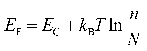 | (4) |
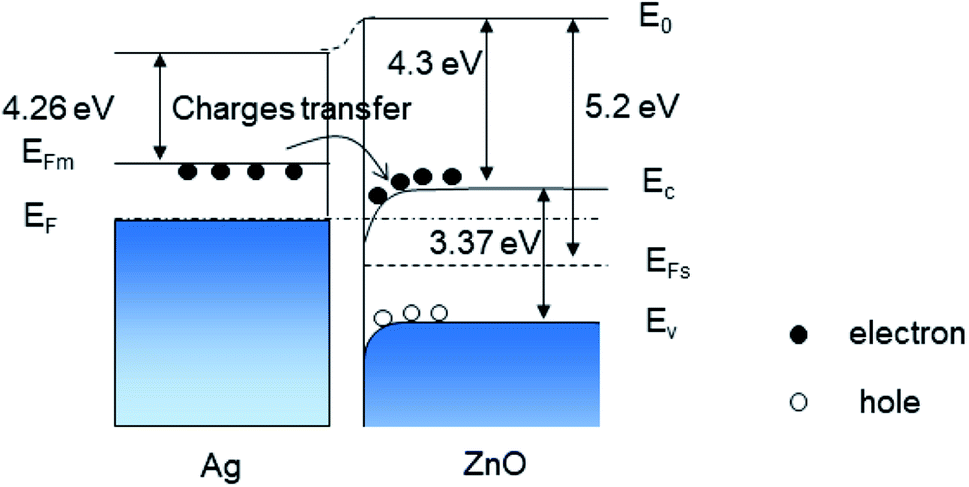 | ||
| Scheme 2 Energy band diagram of ZnO/Ag interface showing the electron transfer between Ag and ZnO.61 | ||
Fig. 3d shows the FTIR spectra for those samples which indicate the chemical structure of MB molecules, ZnO and MB adsorbed on the ZnO surface. A broad band at 3430 cm−1 is attributed to the adsorbed water molecules from moisture. The prominent peaks of MB molecules are realized in the spectra of MB and MB adsorbed on ZnO or ZnO/Ag3. A significant band at 1600 cm−1 results from the skeletal stretching vibration of the C![[double bond, length as m-dash]](https://www.rsc.org/images/entities/char_e001.gif) C and CN bonds in the hetero-cycle of the MB molecules.63 Two bands at 1395 cm−1 and 888 cm−1 belong to C–H bending vibrations.30 In addition, the relative intensities of the absorption peaks from the ZnO/Ag3 + MB sample are lower than those of MB molecules, which implies a strong interaction between MB molecules and the ZnO/Ag substrate.
C and CN bonds in the hetero-cycle of the MB molecules.63 Two bands at 1395 cm−1 and 888 cm−1 belong to C–H bending vibrations.30 In addition, the relative intensities of the absorption peaks from the ZnO/Ag3 + MB sample are lower than those of MB molecules, which implies a strong interaction between MB molecules and the ZnO/Ag substrate.
3.4. TEM, HRTEM and EDS investigations
Based on the TEM image (Fig. 4a), the average nanoplate size of ZnO was 100 nm × 200 nm in lateral length and 10 ÷ 20 nm in width. TEM image reveals that the ZnO NPls overlap with each other to form a three-dimensional network structure. The high-resolution TEM (HRTEM) image in Fig. 4b and e shows that the distance between adjacent lattice fringes is nearly 0.193 nm in ZnO and 0.234 nm in Ag. The TEM image of ZnO/Ag3 (Fig. 4d) exhibits a large number of AgNPs randomly distributed on ZnO NPls, which leads to the better charge transportation of conducting electrons between ZnO and Ag. It has been estimated that the diameter of AgNPs is about 9 nm. The ZnO and ZnO/Ag3 samples were analyzed by EDS and the representative results are given in Fig. 4c and f. Zn and O elements were derived from ZnO nanoplates with contents of 24.91 at% of Zn and 75.09 at% of O, while the ZnO/Ag3 sample was composed of 32.9 at% of Zn, 49.55 at% of O, and 17.55 at% of Ag. | ||
| Fig. 4 (a) Typical TEM and (b) HRTEM images of ZnO, (d) TEM and (e) HRTEM images of ZnO/Ag3 and corresponding spot-profile EDS spectra of (c) pure ZnO, (f) ZnO/Ag3. | ||
3.5. UV-Vis and PL results
UV-Vis measurements were implemented to determine the optical band gaps of these samples. The absorbance of ZnO nanoplates and five kinds of ZnO/Agx hybrids in the range of 350 nm to 450 nm (i.e. ultraviolet-visible region) is displayed in Fig. 5a. All the samples showed a sharp drop in absorbance around the absorption edge. With the increase in Ag amount, the absorption edges of the UV-Vis spectra become obviously red-shifted. An increased absorbance for wavelengths longer than 380 nm was observed in the case of ZnO/Ag5 only. The possible cause of this unusually increased absorbance is not yet understood. A strong band located at around 370 nm in all spectra corresponds to the near-band edge absorption of ZnO. The optical band-gap can be determined by using Tauc's law:64| αhν = A(hν − Eg)n | (5) |
 | ||
| Fig. 5 (a) The UV-Vis absorption spectra of ZnO and ZnO/Agx samples, (b) plot of (αhν)2 versus hν, (c) the band-gap from 2.5 to 3.2 eV, (d) absorption spectra of MB alone (black line), of MB adsorbed on ZnO (red line) and ZnO/Ag3 (dash line). | ||
Fig. 6 shows the photoluminescence (PL) spectra of all the samples. A narrow emission band located at about 380 nm (3.27 eV) can be assigned to the exciton emission that results from the recombination of shallowly trapped charge carriers. A broad emission band at 650 nm was due to oxygen defect states of ZnO structure.37 In comparison with this report,37 the broad emission band of ZnO nanoparticles centered at around 530 nm. Because this emission band highly depends on the size of the ZnO structure, it shifts to a longer wavelength as the size of ZnO nanoplates is much larger than that of ZnO nanoparticles.
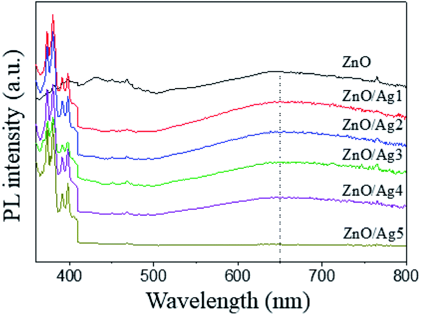 | ||
| Fig. 6 Photoluminescence (PL) spectra of ZnO and ZnO/Ag excited at 345 nm. | ||
3.6. SERS application
SERS spectra of methylene blue adsorbed onto ZnO and ZnO/Ag composite nanomaterials were studied in this research. Fig. 7a shows the Raman spectrum of MB at a concentration of 10−4 M using Si/SiO2 as a substrate. The resolved Raman vibration features of MB, located at around 445, 501, 772, 1037, 1070, 1154, 1302, 1395, 1625 cm−1, agree well with previously reported data.7 The strongest intense band at 1625 cm−1 is attributed to the C–C ring stretching mode of MB molecules.30 The characteristic Raman band of MB molecules at 445 cm−1 is ascribed to the C–N–C skeletal deformation mode. As illustrated in Fig. 7b, ZnO showed little effect on the Raman spectrum enhancement of MB. However, when MB was adsorbed onto ZnO/Agx (x = 1, 2, 3, 4, 5) substrates, a significant increase in SERS signal intensity was observed. Because of the interaction of MB molecules with hot spots on the nanosystems, the locations of the peaks of MB in the normal Raman and SERS substrates are different. The Raman bands of SERS substrates (ZnO and ZnO/Agx) were shifted to lower wavenumbers at 424, 606, 913, 1029, 1120, 1227, 1317, 1436, 1515, and 1613 cm−1 in comparison with the normal Raman of MB. Their SERS peak positions differ from each other due to the quantity of molecules in the hot spot area. The results showed that AgNPs on ZnO NPls significantly increased Raman peak intensity by taking 1613 cm−1 peak as the index. It should be noted that the Raman intensity is highest for ZnO/Ag3 with the same concentration of MB. This is most likely due to ZnO/Ag having the larger surface area compared to the other samples, which allows the probe molecules to anchor and produce higher SERS intensity. Therefore, ZnO/Ag3 was used in the next investigation. | ||
| Fig. 7 Raman spectra of MB on Si substrate (a), MB adsorbed on AgNPs, ZnO NPls, ZnO/Ag (b), MB concentration in all experiments as 10−4 M. | ||
To evaluate the sensitivity of ZnO/Agx, the SERS spectra of MB molecules on ZnO/Agx and ZnO substrates were compared. As shown in Fig. 7b, ZnO/Agx substrates produce a stronger signal enhancement than ZnO substrate. The enhancement factor can be estimated according to the well-known equation:52
 | (6) |
| SERS substrates | ZnO | ZnO/Ag1 | ZnO/Ag2 | ZnO/Ag3 | ZnO/Ag4 | ZnO/Ag5 | |
|---|---|---|---|---|---|---|---|
| Raman peak (cm−1) | 1613 | 2.9 × 10⁴ | 3.7 × 10⁵ | 3.8 × 10⁵ | 4.4 × 10⁵ | 4.1 × 10⁵ | 3.8 × 10⁵ |
| 1515 | 2.1 × 10³ | 1.6 × 10⁶ | 1.7 × 10⁶ | 1.9 × 10⁶ | 1.8 × 10⁶ | 1.6 × 10⁶ | |
| 1436 | 1.6 × 10³ | 5.3 × 10⁶ | 5.4 × 10⁶ | 6.2 × 10⁶ | 6.0 × 10⁶ | 5.6 × 10⁶ | |
| 1317 | 1.7 × 10³ | 1.7 × 10⁶ | 1.8 × 10⁶ | 2.7 × 10⁶ | 2.0 × 10⁶ | 1.7 × 10⁶ | |
| 1227 | 2.2 × 10³ | 1.2 × 10⁶ | 1.2 × 10⁶ | 1.4 × 10⁶ | 1.4 × 10⁶ | 1.2 × 10⁶ | |
| 1120 | 1.7 × 10³ | 1.2 × 10⁶ | 1.2 × 10⁶ | 1.4 × 10⁶ | 1.4 × 10⁶ | 1.2 × 10⁶ | |
| 1029 | 1.5 × 10³ | 1.4 × 10⁶ | 1.3 × 10⁶ | 1.6 × 10⁶ | 1.5 × 10⁶ | 1.4 × 10⁶ | |
| 913 | 1.8 × 10³ | 4.7 × 10⁵ | 4.4 × 10⁵ | 5.3 × 10⁵ | 4.5 × 10⁵ | 4.2 × 10⁵ | |
| 606 | 1.8 × 10³ | 2.9 × 10⁵ | 3.4 × 10⁵ | 3.8 × 10⁵ | 3.4 × 10⁵ | 3.2 × 10⁵ | |
| 424 | 2.0 × 10³ | 1.6 × 10⁵ | 1.7 × 10⁵ | 2.2 × 10⁵ | 1.8 × 10⁵ | 1.6 × 10⁵ | |
According to Table 1, the EF of ZnO/Ag3 is the highest compared to other samples, which is presumably related to MB molecules on high-density hot spots around NPs/NPls surfaces. The shortening of the interface gap junctions between metal and semiconductor enhanced the local electromagnetic field69 and the EF of ZnO/Ag3 is highest at the band of 1436 cm−1 with a value of 6.2 × 10⁶, which is superior to that of 2.9 × 10⁴ obtained in our previous ZnO nanoplates-based SERS-active substrate at a same concentration of MB (10−4 M).30 The strongest Raman band at 1436 cm−1 was related to the N-phenyl stretching vibration in MB molecules. However, for higher Ag amounts (ZnO/Ag4 and ZnO/Ag5), the EF values were reduced due to the screening of Ag to the charge transfer between ZnO and MB molecules.
The SERS activity of ZnO/Ag3 substrate was subsequently investigated at MB concentrations ranging from 10−9 to 10−4 M. As shown in Fig. 8a, the intensity of the spectra becomes gradually stronger as the concentration of MB increases from 10−9 to 10−4 M. The Raman peaks for the concentrations at 10−4 and 10−5 M are highly distinct and whole. When the MB concentration is dropped to 10−9 M, the Raman peaks are reduced, leaving only one peak at 1436 cm−1, and the intensity of remaining peak is also weakened. The Raman peak intensity at 1436 cm−1 for ZnO/Ag3 was correlated with the concentration of MB via the plot of the logarithm of SERS intensity (log![[thin space (1/6-em)]](https://www.rsc.org/images/entities/char_2009.gif) I) versus the logarithm of MB concentration (logC) as depicted in Fig. 8b. Log I increases linearly with the logarithm of the number of MB molecules anchored on the substrate. To estimate the detection limit of pristine ZnO and ZnO/Agx hybrid systems, Raman spectra of MB molecules at a low concentration of 10−9 M was measured. Because of the strong electromagnetic and charge transfer effects, as well as the inter-NPs surface plasmon resonance (SPR) around NPls surface,10 the 1436 cm−1 peak intensity was still significant and distinguishable at low MB concentrations (10−7, 10−8, and 10−9 M). Even at a low concentration (10−9 M) of MB, a distinguishable Raman signal can still be observed, showing that ZnO/Ag3 has a high SERS activity. However, qualitative analysis below this low concentration is difficult to realize. The limit of detection (LOD) of MB using ZnO/Ag3 nanosystem can be achieved as 10−9 M, much better than that of a pristine ZnO-based SERS substrate (10−4 M).30 Moreover, the detection limit of molecular probes increases due to the polarization of the excitation laser at the rough ZnO/Ag surface.70 This result agrees with some other reports.52,53 Some detection limits of pristine ZnO and ZnO/metal-based SERS substrate were compared and listed in Table 2.
I) versus the logarithm of MB concentration (logC) as depicted in Fig. 8b. Log I increases linearly with the logarithm of the number of MB molecules anchored on the substrate. To estimate the detection limit of pristine ZnO and ZnO/Agx hybrid systems, Raman spectra of MB molecules at a low concentration of 10−9 M was measured. Because of the strong electromagnetic and charge transfer effects, as well as the inter-NPs surface plasmon resonance (SPR) around NPls surface,10 the 1436 cm−1 peak intensity was still significant and distinguishable at low MB concentrations (10−7, 10−8, and 10−9 M). Even at a low concentration (10−9 M) of MB, a distinguishable Raman signal can still be observed, showing that ZnO/Ag3 has a high SERS activity. However, qualitative analysis below this low concentration is difficult to realize. The limit of detection (LOD) of MB using ZnO/Ag3 nanosystem can be achieved as 10−9 M, much better than that of a pristine ZnO-based SERS substrate (10−4 M).30 Moreover, the detection limit of molecular probes increases due to the polarization of the excitation laser at the rough ZnO/Ag surface.70 This result agrees with some other reports.52,53 Some detection limits of pristine ZnO and ZnO/metal-based SERS substrate were compared and listed in Table 2.
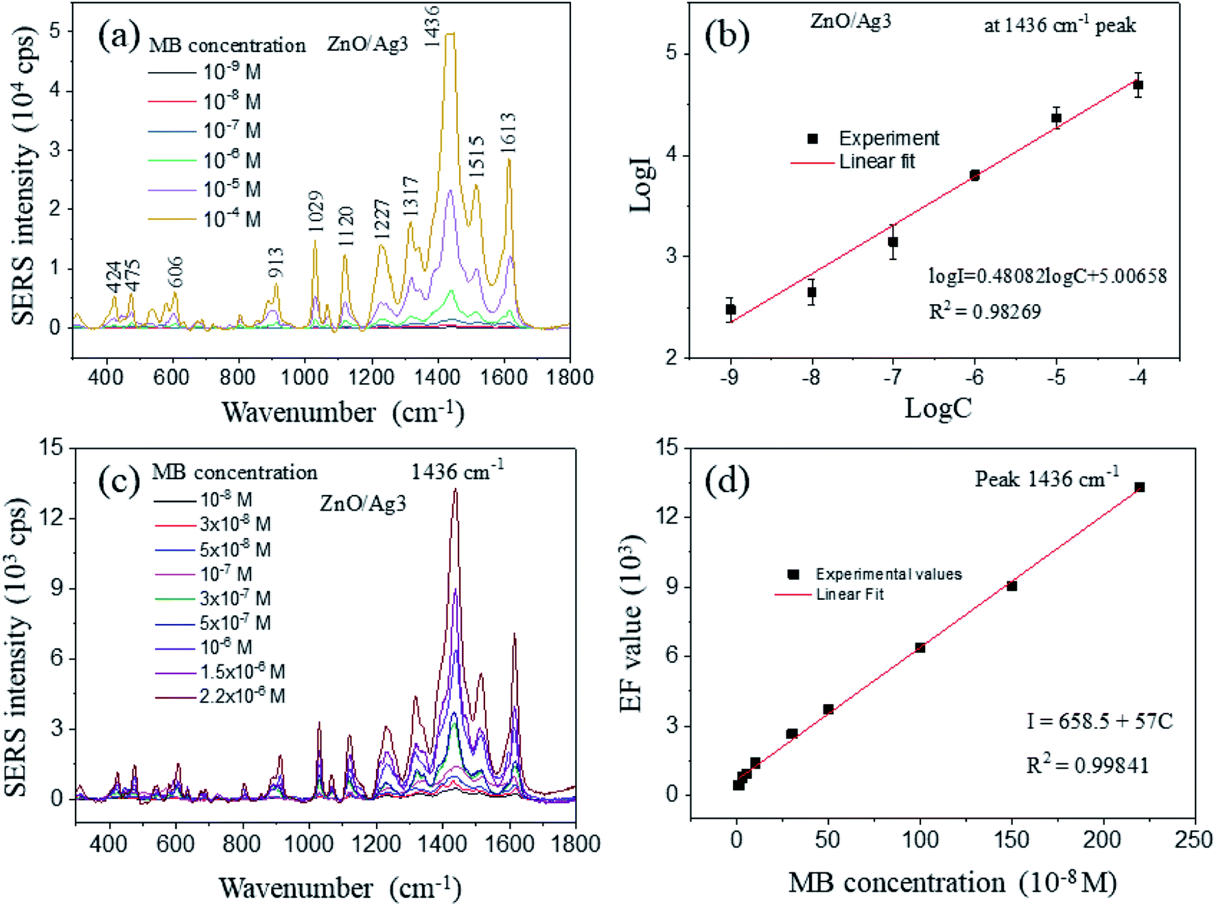 | ||
| Fig. 8 (a) Raman spectra of MB adsorbed on ZnO/Ag3 at concentrations ranging from 10−9 M to 10−4 M, (b) the linear relationship between the log I and log C of the 1436 cm−1 peak, where I is the SERS intensity and C is the MB concentration, (c) Raman spectra of MB adsorbed on ZnO/Ag3 with different concentrations from 10−8 M to 2.2 × 10⁻⁶ M, (d) the linear relationship between SERS intensity and MB concentration. | ||
| SERS substrate | Target species | LOD | Reference |
|---|---|---|---|
| ZnO nanoplates/Ag nanoparticles | MB | 10−9 M | This work |
| ZnO nanoplates | MB | 10−4 M | 30 |
| ZnO nanorods | Acetaminophen | 10−4 M | 68 |
| ZnO nanoplates/Ag nanoparticles | R6G | 10−7 M | 49 |
| ZnO nanorods/Ag nanoparticles | Melamine | 10−10 M | 16 |
| ZnO nanorods/Ag nanoparticles | Abamectin | 1 ppm | 14 |
| ZnO nanorods/Ag nanoparticles | R6G | 10−16 M | 15 |
| ZnO nanorods/Ag nanoparticles | R6G | 10−6 M | 71 |
| ZnO nanowires/Au nanoparticles | R6G | 10−7 M | 72 |
| ZnO nanospheres/Ag nanoparticles | R6G | 10−8 M | 53 |
| ZnO sea urchin/Ag nanoparticles | R6G | 10−16 M | 52 |
| ZnO microrods/Au core@Ag shell | 4-ATP | 10−6 M | 73 |
Thanks to the highest SERS signal from the ZnO/Ag3 sample, the SERS activity of ZnO/Ag3 was subsequently investigated at MB concentrations ranging from 10−8 M to 2.2 × 10⁻⁶ M (Fig. 8c). In this narrow range of MB concentration, there is a linear relationship between the SERS intensity of 1436 cm−1 peak and MB concentration that was displayed in Fig. 8d. The linear fitting equation is approximated as:
| I = 658.5 + 57C | (7) |
3.7. SERS mechanisms
On the noble metal substrate, both electromagnetic and chemical enhancement contribute to SERS activity. The former is caused by the surface plasmon resonance based on the interaction of the electric field of surface plasmons with the transition moment of the adsorbed molecules. The latter is due to the charge-transfer between the adsorbate and the substrate. In contrast, in semiconductor materials, electromagnetic enhancement is referred to as exciton resonance rather than surface plasmon resonance.29 The assembly of silver nanoparticles onto a two-dimensional semiconductor may induce synergistic effects in electromagnetic and chemical enhancement, thereby improving the detection limit of SERS. For the hybrid structure composed of ZnO nanoplates and Ag nanoparticles, the metal–semiconductor junction creates a changeable local EM field at the interface of the nanosystem, which prevents the recombination of electron–hole pairs. EM enhancement depends on the number of hot spots in the substrate, which is a strongly enhanced field at the contact region between the AgNPs and ZnO NPls. Hot spots can also be produced through interaction between AgNPs or from the narrow junctions between closely spaced NPs. A combined EM and chemical effect is induced at the edges of the Ag nanocavities.74 The increased roughness of AgNPs on ZnO NPls may enlarge LSPR near the NPs/NPls junction.71,72,75 The coupling of AgNPs provides a significant EM effect at the interfaces of AgNPs/ZnO NPls. The electromagnetic enhancement could work over a long distance and no chemical bond was needed, while chemical enhancement could only work over a short distance and need a chemical bond to charge transfer.73 The ionic size of Zn2+ is 0.74 Å and the bond length of Zn–O is 1.97 Å.59 Fig. 5d shows an absorption band centered at 600 nm in the UV-Vis spectra of MB adsorbed on ZnO and ZnO/Ag3. This band can be attributed to the interaction between MB molecules and ZnO, which results in the formation of a charge transfer band, one of the main factors of SERS behavior in ZnO/Agx systems. The charge transfer mechanism between ZnO and MB can occur as follows: electrons transfer from the valence band (VB) of ZnO to the lowest unoccupied molecular orbital (LUMO) of MB, electrons are excited from the highest occupied molecular orbital (HOMO) of MB to the conduction band (CB) of ZnO, electrons at defect states of ZnO (such as zinc vacancy defect, zinc interstitial defect, oxygen vacancy defect) are excited to CB of ZnO and then injected into LUMO of MB, electron at defect states of ZnO can transfer directly to LUMO of MB.76 ZnO is an n-type semiconductor with a lot of surface defect states called trap states. The energy of laser excitation may promote electron transitions from the trap states into the CB or from the VB to the trap states.77 Electrons can also transfer from the defect state of ZnO due to oxygen vacancy to the LUMO of MB, which is caused by the electronic coupling between MB molecules and ZnO. The Fermi-level of silver (EF = 0.15 V) is more positive than the conduction band of ZnO, thus once the silver islands are formed onto ZnO nanoplates, electrons will shift from the silver nanoparticles to the conduction band of ZnO to reach the same Fermi energy level (EF) between Ag and ZnO.52 The overwhelming storage of electrons on the ZnO results in the formation of an internal electric field, causing a downward band bend on the ZnO side and forming a depletion layer on the Ag side. This also causes the formation of a local electric field around the AgNPs, which can enhance the localized electromagnetic field and improve the Raman scattering of the analytes. The charge transfer leads to a charge distribution difference between the two sides of the interface, which creates the potential barrier, providing an energetic driving force for transferring electrons. As a result, when ZnO/Ag is used as a SERS substrate in detecting MB, MB molecules will obtain electrons from silver nanoparticles rather than the ZnO nanoplate surface. The charge transfer from metal to target molecule may explain the tremendous enhancement of the Raman signal strength of MB adsorbed to ZnO/Ag. In addition, the large surface area of ZnO/Agx may result in contact with more probe molecules on the ZnO/Ag hybrids, which aids in the improvement of SERS. The metal–semiconductor hybrid nanosystem has high sensitivity and is appropriate for trace detection of target molecules.To evaluate the effectiveness of the ZnO/Agx hybrid as a SERS substrate, two factors, sensitivity and reproducibility, must be validated. The relative standard deviation (RSD) of the major peaks is used to estimate the reproducibility of the SERS signals. Fig. 9 exhibited the SERS contours of ZnO/Ag3 to examine the SERS uniformity, which was conducted from point-to-point for various MB molecular concentrations (0.01 ppm, 0.2 ppm, 0.8 ppm, and 6 ppm). 10 tested spots were randomly selected on the ZnO/Ag3 substrate within the Raman shift range of 400–1800 nm, the intensities of SERS spectra exhibit negligible change. The RSD value for the signal intensities of the major SERS peaks was calculated by formula51 to quantitatively assess their uniformity. The maximum RSD at 1436 cm−1 peak was less than 4.8%, revealing that the substrates possess good reproducibility across the entire surface area. Accordingly, it is reasonable to believe that the ZnO/Ag3 hybrid performs SERS substrate with high sensitivity and good reproducibility.
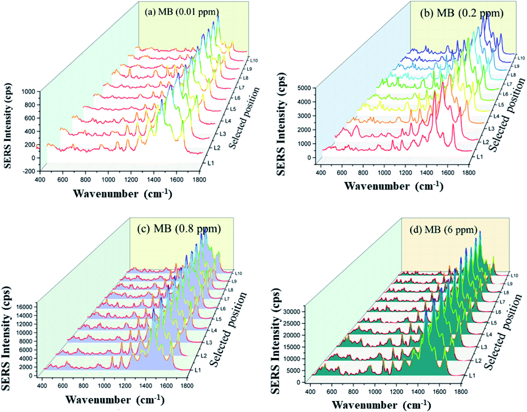 | ||
| Fig. 9 SERS spectra of varied MB concentrations ((a) 0.01 ppm, (b) 0.2 ppm, (c) 0.8 ppm, and (d) 6 ppm) were gathered at 10 randomly selected positions. | ||
4. Conclusions
In our research, the ZnO/Ag hybrid nanosystem was synthesized via hydrothermal treatment followed by chemical reduction without any organic additives. Firstly, ZnO nanoplates with 20 nm in thickness and 100 × 200 nm in lateral size were successfully obtained through the reaction of zinc acetate and sodium hydroxide under hydrothermal condition. Secondly, silver nanoparticles with 9 nm in average diameter were deposited onto ZnO nanoplates via chemically reducing silver nitrate by trisodium citrate. Thanks to the introduction of AgNPs, the Raman intensity of MB molecules was significantly enhanced. The highest EF value for MB (10−4 M) reached 6.2 × 10⁶ for the peak at 1436 cm−1 and the LOD of MB can be observed as 10−9 M for ZnO/Ag3. Additionally, the maximum value for the RSD below 4.8% indicated that the substrate was well uniform, and the limit of detection as 10−9 M MB concentration showed that the nanohybrid possessed high sensitivity. These properties enable ZnO/Ag substrate to be suitable for the trace detection of MB molecules. This research has contributed to a better understanding of the synergistic mechanism of chemical and electromagnetic enhancements of the SERS substrate based on the combination of semiconductor with noble metal materials. In the follow-up research, we will investigate the SERS enhancement of ZnO/Ag hybrid materials in detecting other molecules such as methyl orange (MO), methyl red (MR), rhodamine B (RhB), etc.Conflicts of interest
There are no conflicts of interest to declare.Acknowledgements
This research was supported by a project of the TNU-University of Sciences in Vietnam under grant number CS2021-TN06-11.References
- K.-L. Bae, J. Kim, C. K. Lim, K. M. Nam and H. Song, Nat. Commun., 2017, 8, 1156 CrossRef PubMed.
- G. Nagaraju, S. Udayabhanu, S. A. Prashanth, M. Shastri, K. V. Yathish, C. Anupama and D. Rangappa, Mater. Res. Bull., 2017, 94, 54–63 CrossRef CAS.
- Y. V. Kaneti, Q. M. D. Zakaria, Z. Zhang, C. Chen, J. Yue, M. Liu, X. Jiang and A. Yu, J. Mater. Chem. A, 2014, 2, 13283–13292 RSC.
- Y. Bu and S.-W. Lee, Int. J. Nanomed., 2015, 10, 47–54 CAS.
- S. D. Roy, M. Ghosh and J. Chowdhury, J. Raman Spectrosc., 2015, 46, 451–461 CrossRef.
- R. S. Sarmara, A. Daneshfar and R. Sahrai, J. Ind. Eng. Chem., 2011, 17, 533–536 CrossRef.
- C. Li, Y. Huang, K. Lai, B. A. Rasco and Y. Fan, Food Control, 2016, 65, 99–105 CrossRef CAS.
- Y.-J. Xu, X.-H. Tian, X.-Z. Zhang, X.-H. Gong, H.-H. Liu, H.-J. Zhang, H. Huang and L.-M. Zhang, J. Chromatogr. Sci., 2012, 50, 591–597 CAS.
- Y. Zhang, Z. Wang, L. Wu, Y. Pei, P. Chen and Y. Cui, Anal, 2014, 139, 5148–5154 RSC.
- K. Sivashanmugan, J.-D. Liao, B. H. Liu, C.-K. Yao and S.-C. Luo, Sens. Actuators, B, 2015, 207, 430–436 CrossRef CAS.
- J. Huang, D. Ma, F. Chen, M. Bai, K. Xu and Y. Zhao, Anal. Chem., 2015, 87, 10527–10534 CrossRef CAS PubMed.
- E. Vinogradova, A. Tlahuice-Flores, J. J. Velazquez-Salazar, E. Larios-Rodriguez and M. Jose-Yacaman, J. Raman Spectrosc., 2014, 45, 730–735 CrossRef CAS.
- H. Chi, C. Wang, Z. Wang, H. Zhu, V. S. D. Mesias, X. Dai, Q. Chen, W. Liu and J. Huang, Anal, 2020, 145, 5158–5165 RSC.
- N. H. Ke, N. H. Thanh, N. H. Long, D. A. Tuan and L. V. T. Hung, J. Mater. Sci.: Mater. Electron., 2021, 32, 27318–27332 CrossRef CAS.
- A. K. Pal, S. Pagal, K. Prashanth, G. K. Chandra, S. Umapathy and D. B. Mohan, Sens. Actuators, B, 2019, 279, 157–169 CrossRef CAS.
- Z. Yi, Y. Yi, J. Luo, X. Li, X. Xu, X. Jiang, Y. Yi and Y. Tang, Phys. B, 2014, 451, 58–62 CrossRef CAS.
- R. R. Naujok, R. V. Duevel and R. M. Corn, Langmuir, 1993, 9, 1771–1774 CrossRef CAS.
- O. Olea-Mejia, M. Fernandez-Mondragon, G. R.-d. l. Concha and M. Camacho-Lopez, Appl. Surf. Sci., 2015, 348, 66–70 CrossRef CAS.
- G. Barbillon, Coat, 2019, 9, 86 CrossRef.
- M. E. Koleva, N. N. Nedyalkov, R. Nikov, R. Nikov, G. Atanasova, D. Karashanova, V. I. Nuzhdin, V. F. Valeev, A. M. Rogov and A. L. Stepanov, Appl. Surf. Sci., 2020, 508, 145227 CrossRef CAS.
- T. T. H. Pham, N. D. Dien and X. H. Vu, RSC Adv., 2021, 11, 21475–21488 RSC.
- T. T. H. Pham, X. H. Vu, N. D. Dien, T. T. Trang, N. V. Truong, T. D. Thanh, P. M. Tan and N. X. Ca, RSC Adv., 2020, 10, 24577–24594 RSC.
- X. H. Vu, N. D. Dien, T. T. H. Pham, T. T. Trang, N. X. Ca, P. T. Tho, N. D. Vinh and P. V. Do, RSC Adv., 2020, 10, 38974–38988 RSC.
- X. H. Vu, N. D. Dien, T. T. H. Pham, N. V. Truong, N. X. Ca and V. V. Thu, RSC Adv., 2021, 11, 14596–14606 RSC.
- X. Zhou, Y. Xiao, M. Wang, P. Sun, F. Liu, X. Liang, X. Li and G. Lu, ACS Appl. Mater. Interfaces, 2015, 7, 8743–8749 CrossRef CAS PubMed.
- X. Hu, G. Meng, Q. Huang, W. Xu, F. Han, K. Sun, Q. Xu and Z. Wang, Nanotechnol, 2012, 23, 385705 CrossRef PubMed.
- L. Yang, X. Jiang, W. Ruan, B. Zhao, W. Xu and J. R. Lombardi, J. Phys. Chem. C, 2008, 112, 20095–20098 CrossRef CAS.
- C. Liu, X. Xu, C. Wang, G. Qiu, W. Ye, Y. Li and D. Wang, Sens. Actuators, B, 2020, 307, 127634 CrossRef.
- J. R. Lombardi and R. L. Birke, J. Phys. Chem. C, 2014, 118, 11120–11130 CrossRef CAS.
- T. T. H. Pham, X. H. Vu, T. T. Trang, N. X. Ca, N. D. Dien, P. V. Hai, N. T. H. Lien, N. T. Nghia and T. T. K. Chi, Opt. Mater., 2021, 120, 111460 CrossRef CAS.
- J. J. Richardson and F. F. Lange, Cryst. Growth Des., 2009, 9, 2570–2575 CrossRef CAS.
- J. J. Richardson and F. F. Lange, Cryst. Growth Des., 2009, 9, 2576–2581 CrossRef CAS.
- D. Barreca, A. Gasparotto and E. Tondello, J. Mater. Chem., 2011, 21, 1648–1654 RSC.
- X. Wen, W. Wu, Y. Ding and Z. L. Wang, J. Mater. Chem., 2012, 22, 9469–9476 RSC.
- P. Li, X. Wang, X. Zhang, L. Zhang, X. Yang and B. Zhao, Front. Chem., 2019, 7, 144 CrossRef CAS PubMed.
- L. T. T. Nguyen, L. T. H. Nguyen, A. T. T. Duong, B. D. Nguyen, N. Q. Hai, V. H. Chu, T. D. Nguyen and L. G. Bach, Mater, 2019, 12, 1195 CrossRef CAS PubMed.
- T. Bora, K. K. Lakshman, S. Sarkar, A. Makhal, S. Sardar, S. K. Pal and J. Dutta, Beilstein J. Nanotechnol., 2013, 4, 714–725 CrossRef CAS PubMed.
- S. Wi, H. Woo, S. Lee, J. Kang, J. Kim, S. An, C. Kim, S. Nam, C. Kim and B. Park, Nanoscale Res. Lett., 2015, 10, 204 CrossRef PubMed.
- S. Boubenia, A. S. Dahiya, G. Poulin-Vittrant, F. Morini, K. Nadaud and D. Alquier, Sci. Rep., 2017, 7, 15187 CrossRef CAS PubMed.
- J. Zhou, K. Nomenyo, C. C. Cesar, A. Lusson, A. Schwartzberg, C.-C. Yen, W.-Y. Woon and G. Lerondel, Sci. Rep., 2020, 10, 4237 CrossRef CAS PubMed.
- D. D. Nguyen, D. T. Do, X. H. Vu, D. V. Dang and D. C. Nguyen, Adv. Nat. Sci.: Nanosci. Nanotechnol., 2016, 7, 015004 Search PubMed.
- F. Khurshid, M. Jeyavelan, M. S. L. Hudson and S. Nagarajan, R. Soc. Open Sci., 2019, 6, 181764 CrossRef CAS PubMed.
- A. Amutha, S. Amirthapandian, B. Sundaravel, B. K. Panigrahi, K. Saravanan and P. Thangadurai, J. Appl. Phys., 2016, 120, 205104 CrossRef.
- D. Cao, S. Gong, X. Shu, D. Zhu and S. Liang, Nanoscale Res. Lett., 2019, 14, 210 CrossRef PubMed.
- P. Borade, K. U. Joshi, A. Gokarna, G. Lerondel, P. Walke, D. Late and S. M. Jejurikar, Mater. Chem. Phys., 2016, 169, 152–157 CrossRef CAS.
- P. Borade, K. U. Joshi, A. Gokarna, G. Lerondel and S. M. Jejurikar, Nanotechnol, 2016, 27, 025602 CrossRef CAS PubMed.
- J. Han, F. Fan, C. Xu, S. Lin, M. Wei, X. Duan and Z. L. Wang, Nanotechnol, 2010, 21, 405203 CrossRef PubMed.
- X. Han and B. Zhao, Molecular and Laser Spectroscopy–Chapter 10: Surface-Enhanced Raman Scattering (SERS) and Applications, Elsevier Inc., 2020, pp. 349–386 Search PubMed.
- K. Liu, D. Li, R. Li, Q. Wang, S. Pan, W. Peng and M. Chen, J. Mater. Res., 2013, 28, 3374–3383 CrossRef CAS.
- A. Muravitskaya, A. Rumyantseva, S. Kostcheev, V. Dzhagan, O. Stroyuk and P.-M. Adam, Opt. Express, 2016, 24, 168–173 CrossRef PubMed.
- N. Li, Z. Hao, H. Cao, L. Guo, H. Cao, N. Li, Y. Yang, T. Jiao, H. Liu and M. Wang, Opt. Laser Technol., 2022, 148, 107765 CrossRef.
- R. Li, C. Han and Q.-W. Chen, RSC Adv., 2013, 3, 11715–11722 RSC.
- Y. Zang, J. Yin, X. He, C. Yue, Z. Wu, J. Li and J. Kang, J. Mater. Chem. A, 2014, 2, 7747–7753 RSC.
- Y. Feng, Y. Wang, H. Wang, T. Chen, Y. Y. Tay, L. Yao, Q. Yan, S. Li and H. Chen, Small, 2012, 8, 246–251 CrossRef CAS PubMed.
- I. Alessandri and J. R. Lombardi, Chem. Rev., 2016, 116, 14921–14981 CrossRef CAS PubMed.
- L. Yang, Y. Yang, Y. Ma, S. Li, Y. Wei, Z. Huang and N. V. Long, Nanomater, 2017, 7, 398 CrossRef PubMed.
- U. Ozgur, Y. I. Alivov, C. Liu, A. Teke, M. A. Reshchikov, S. Dogan, V. Avrutin, S. J. Cho and H. Morkoc, J. Appl. Phys. Rev., 2005, 98, 041301 CrossRef.
- C. Bundesmann, N. Ashkenov, M. Schubert, T. Butz, E. M. Kaidashev, M. Lorenz and M. Grundmann, Appl. Phys. Lett., 2003, 83, 1974–1976 CrossRef CAS.
- S. D. Shinde, A. V. Deshmukh, S. K. Date, V. G. Sathe and K. P. Adhi, Thin Solid Films, 2011, 520, 1212–1217 CrossRef CAS.
- R. Zamiri, A. Rebelo, G. Zamiri, A. Adnani, A. Kuashai, M. S. Belsley and J. M. F. Ferreira, RSC Adv., 2014, 4, 20902–20908 RSC.
- J. Yin, Y. Zang, C. Yue, Z. Wu, S. Wu, J. Li and Z. Wu, J. Mater. Chem., 2012, 22, 7902–7909 RSC.
- H. Tang, G. Meng, Q. Huang, Z. Zhang, Z. Huang and C. Zhu, Adv. Funct. Mater., 2012, 22, 218 CrossRef CAS.
- O. V. Ovchinnikov, A. V. Evtukhova, T. S. Kondratenko, M. S. Smirnov, V. Y. Khokhlov and O. V. Erina, Vib. Spectrosc., 2016, 86, 181–189 CrossRef CAS.
- J. Tauc, Optical Properties of Amorphous Semiconductors, Plenum Publishing Company Ltd., 1974, pp. 159–220 Search PubMed.
- E. Burstein, Phys. Rev., 1954, 93, 632–633 CrossRef CAS.
- T. S. Moss, Proc. Phys. Soc., London, Sect. B, 1954, 67, 775–782 CrossRef.
- Z. Hao, N. Li, H. Cao, L. Guo, H. Cao, N. Li, L. Cao, H. L. Liu, T. Jiao and M. Wang, J. Lumin., 2022, 243, 118684 CrossRef CAS.
- X. Wang, G. She, H. Xu, L. Mu and W. Shi, Sens. Actuators, B, 2014, 193, 745–751 CrossRef CAS.
- D. Natelson, Y. Li and J. B. Herzog, Phys. Chem. Chem. Phys., 2013, 15, 5262–5275 RSC.
- J. Elias, M. Gizowska, P. Brodard, R. Widmer, Y. deHazan, T. Graule, J. Michler and L. Philippe, Nanotechnol, 2012, 23, 255705 CrossRef PubMed.
- G. Shan, S. Zheng, S. Chen, Y. Chen and Y. Liu, Colloids Surf., B, 2012, 94, 157–162 CrossRef CAS PubMed.
- Y. F. Chan, H. J. Xu, L. Cao, Y. Tang, D. Y. Li and X. M. Sun, J. Appl. Phys., 2012, 111, 033104 CrossRef.
- Y. Luo, Colloid J., 2009, 71, 223–232 CrossRef CAS.
- C.-K. Yao, J.-D. Liao, C.-H. Lin, Y.-S. Yang, S.-H. Yu and J.-W. Yang, Sens. Actuators, B, 2014, 191, 219–226 CrossRef CAS.
- X. Li, H. Hu, D. Li, Z. Shen, Q. Xiong, S. Li and H. J. Fan, ACS Appl. Mater. Interfaces, 2012, 4, 2180–2185 CrossRef CAS PubMed.
- Z. Zhang, Y. Yu and P. Wang, ACS Appl. Mater. Interfaces, 2012, 4, 990–996 CrossRef CAS PubMed.
- D. Cavalcoli, B. Fraboni and A. Cavallini, Semicond. Semimetals, 2015, 91, 251–278 Search PubMed.
| This journal is © The Royal Society of Chemistry 2022 |