DOI:
10.1039/D1MA01078F
(Paper)
Mater. Adv., 2022,
3, 2827-2837
Emulating the short-term plasticity of a biological synapse with a ruthenium complex-based organic mixed ionic–electronic conductor†
Received
16th November 2021
, Accepted 9th February 2022
First published on 16th February 2022
Abstract
Short-term plasticity (STP) is a phenomenon in the biological brain where the synaptic weight changes depending solely on the presynaptic activity in the biological brain. STP is an essential brain function for processing of short-term temporal information. Implementation of STP as an electronic device requires mimicking the dynamic behavior of calcium-induced neurotransmitters at presynaptic terminals. This study provides an organic mixed ionic–electronic conductor (OMIEC) memristor based on Ru(bpy)3(PF6)2 as an organic active layer to mimic the STP of a biological synapse. The behavior of the neurotransmitters was emulated through the drift and diffusion of mobile ions in the OMIEC active layer. The ion conductivity of the OMIEC memristor was tuned by adding the LiClO4 salt, which affects the short-term memory behavior. Specifically, our OMIEC memristor exhibited a timescale of paired-pulse facilitation decay similar to that of biological synapses with the addition of 2 wt% salt. Furthermore, the device containing 2 wt% LiClO4 showed similar recovery timescales to a biological synapse when 4 + 1 spikes were applied for emulating the short-term synaptic plasticity. Lastly, our OMIEC memristors were employed as the STP component of a SPICE simulation to modulate the spike-timing-dependent synaptic plasticity learning rule by combining with a non-volatile memristor.
1. Introduction
With the growth of big data technologies in recent years, conventional computing systems encounter the fundamental limitations of von Neumann architecture such as energy and speed penalties originating from the data movement between the processing unit and memory.1–4 Alternatively, more efficient computing frameworks are found in biological brain systems performing analog computations through massively parallel networks of neurons and synapses. Inspired by the computing in the brain, which stores the synaptic weight and simultaneously regulates signal transmission, the idea of neuromorphic computing was introduced in 1990 by Carver Mead and has been researched for decades.5,6
On one hand, complementary metal-oxide-semiconductor (CMOS) based neuromorphic devices have been developed to emulate event-driven and large-scale spiking neural networks with highly efficient computing architectures.7,8 Such architectures have been applied in neuromorphic hardware designs like Neurogrid, BrainScaleS, TrueNorth, SpiNNaker, and Loihi.9–13 Despite this remarkable progress, there are crucial challenges for CMOS-based neuromorphic devices in terms of scalability and power consumption as an ideal neuromorphic system.14,15 On the other hand, a new class of emerging neuromorphic devices, namely a memristor or resistive random access memory (ReRAM), has been vigorously investigated. Memristors encode information in their resistance states according to the history of applied stimulations through the physical mechanism of ion or oxygen vacancy drift.16–18 Therefore, long-term plasticity (LTP) and short-term plasticity (STP), which are the fundamental properties of biological synapses, can be implemented using memristive devices. In a biological system, LTP is regarded as a primary cellular substrate for learning and memory owing to its non-volatile characteristics, while STP is generally considered to perform a crucial computational role because its memory lasts only seconds to minutes.6 The development of memristive devices has primarily focused on emulating the LTP through the formation of conducting filaments composed of metal ions or oxygen vacancies. Many research groups implemented LTP by using memristors such as Ag/Si, SiNx/a-Si, TiN/TaOx, TiOx/Al2O3, and HfOx/AlOx based devices.19–23 However, a relatively small number of STP-based memristors have been developed, although their volatile characteristics can be used in spatio-temporal or reservoir computing in recurrent neural networks.24,25 STP memristors are also potentially applicable to a synaptic memory, which comprises both long-term and short-term partitions, to improve the learning efficiency.26 Wang et al. demonstrated short-term memory (STM) properties using a SiOxNy/Ag diffusive memristor, but the device showed a too short relaxation time than biological synapses.27 The STP behavior can also be found in a GeSe/Ag based memristor. However, their uncontrollable weak filament possibly makes incoherent experimental data.28
In this study, we mimic for the first time the STP properties of biological synapses using an organic mixed ionic–electronic conductor (OMIEC) memristor. OMIECs have been used in various applications such as batteries, light-emitting devices, transistors, sensors, and neuromorphic devices.29–33 Interestingly, several research groups have reported the LTP behavior of OMIEC-based memristors, but the STP behavior has not been demonstrated yet although some OMIEC materials can be employed as STP-based memristors due to their operational mechanisms similar to biological synapses.34,35 In this study, a ruthenium complex, Ru(bpy)3(PF6)2, with varying salt concentrations was used as an active layer of OMIEC memristors. This ruthenium complex has been widely studied and used in light-emitting devices.36–41 Our OMIEC memristor showed tunable memristive performance by easily changing the concentration of LiClO4. Also, the optimized OMIEC memristor indicated the timescales of paired-pulse facilitation decay and recovery similar to a biological synapse. These advantages make our OMIEC memristor a good candidate for the STP-based neuromorphic device. The ion conductivities of our OMIEC memristors were extracted from electrochemical impedance spectroscopy measurements and found to be closely correlated with the salt concentration. The current–voltage characteristics, turn-on time, relaxation time, and PPF indices of OMIEC memristors are described as well to explain the correlation with biological synaptic properties. Additionally, short-term synaptic plasticity is emulated by applying 4 + 1 spikes and measuring current to confirm the STP characteristics of our memristive devices. Finally, the OMIEC memristors were used as the STP component of a SPICE simulation to modulate the spike-timing-dependent synaptic plasticity (STDP) learning rule by combining with a long-term memory memristive device.
2. Experimental section
2.1. Preparation of the active layer solution
Tris(2,2′-bipyridine)ruthenium(II)hexafluorophosphate (Ru(bpy)3(PF6)2), lithium perchlorate (LiClO4), and acetonitrile were purchased from Sigma-Aldrich and used as received. Active layers consisted of Ru(bpy)3(PF6)2 with various concentrations of the LiClO4 salt additive. Ru(bpy)3(PF6)2 and LiClO4 solutions were separately prepared at the same concentration of 40 mg mL−1 in acetonitrile and mixed at a ratio by weight noted37. The mixed solution was kept under stirring overnight at room temperature and then filtered through a 0.2 μm PTFE membrane filter.
2.2. Device fabrication process
The overall OMIEC memristive device composition is as follows: ITO/PEDOT:PSS/active layer/Pd/Al. Indium tin oxide (ITO; 150 nm thick) coated glass substrates were cleaned with deionized water, acetone, and isopropyl alcohol. Then, the substrates were treated with oxygen plasma cleaning for 15 min. Poly(3,4-ethylenedioxythiophene):poly(styrenesulfonate) (PEDOT:PSS; Clevios PH 1000) filtered through a 0.45 μm nylon filter was spin-coated onto the ITO substrates at 3000 rpm for 30 s, followed by thermal annealing on a hot plate at 120 °C for 15 min, yielding a 50 nm thick film. The active layer solutions were then spin-coated onto the PEDOT:PSS layers at 1500 rpm for 30 s. After the spin coating process of the active layer, the obtained films were annealed at 120 °C for 2 h under a nitrogen atmosphere. The Ru(bpy)3(PF6)2 films with or without LiClO4 were generally 100 nm thick. Finally, the devices were completed with the deposition of 5 nm thick Pd and 200 nm thick Al films through electron beam evaporation. All the spin-coating processes were carried out in ambient atmosphere, and the rest of the processes were performed in a nitrogen atmosphere. The device size was 0.007 cm2 in the shape of a circle.
2.3. Characterization
The ionic conductivities of the devices were measured by electrochemical impedance spectroscopy using a Solartron SI-1260 gain/phase analyzer. The impedance of the devices were measured with an alternating voltage (100 mV amplitude) in the frequency range from 1 Hz to 106 Hz. Impedance spectra were then fitted using MATLAB (R2021a). The other electrical characterization studies were conducted using a Keithley 4200 semiconductor parameter analyzer connected with a probe station under a nitrogen atmosphere.
2.4. STDP SPICE simulation
LTspice (17.0.22.0) was used to simulate the STDP learning rule by employing an OMIEC memristor as a STM fitted with a volatile memory model (VM model) and an electrochemical metallization (ECM) device as a long-term memory (LTM) fitted with a Yakopcic model.20,42–44 These two devices are connected in a series circuit to conduct a SPICE simulation for STDP curves by applying two consecutive pulses. Each pulse is composed of a short-duration pulse with a high amplitude (500 μs with 14 V for a presynaptic spike or 500 μs with 18 V for a postsynaptic spike) and a long-duration pulse with a low amplitude (200 ms and 6 V).
3. Results and discussion
3.1. Analogy between the OMIEC memristor and biological synapses
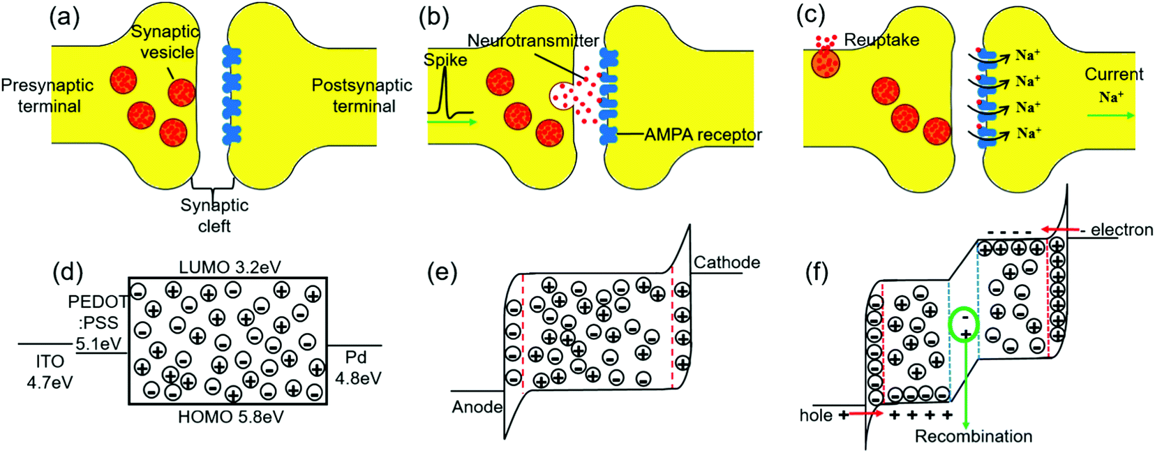
Fig. 1 shows similar operational mechanisms between a biological synapse and a ruthenium complex-based OMIEC memristive device. In a biological system, neurotransmitters were initially stored in synaptic vesicles as shown in Fig. 1a, which corresponds to the primary state of the OMIEC memristor as shown in Fig. 1d. The activation of the presynaptic neuron, i.e., a spike arrival in the biological presynaptic terminal, causes voltage-gated calcium channels to open. Then the internal calcium ion concentration increases, which makes the neurotransmitters to be released into the synaptic cleft and pile up on the AMPA receptors located in the postsynaptic membrane as shown in Fig. 1b.45 Similarly, applying an external voltage to the OMIEC memristor makes cations and anions migrate to the respective interfaces between the active layer and electrodes as shown in Fig. 1e. In turn, the accumulation of ions leads to the formation of electrical double layers (EDLs) at the electrode interfaces, which results in a strong bending of the energy level due to the high charge concentrations at the interfaces.46Fig. 1c illustrates that the neurotransmitters in the biological system trigger the opening of the AMPA ion channels, and thus particular positive ions can travel into the postsynaptic terminal to deliver a spike signal.47 Likewise, applying a sufficiently high voltage to the OMIEC memristive device can lead to the accumulation of more ions on the electrode surfaces, which leads to a sharper and narrower electric field at the interfaces. Subsequently, the injection of electrons and holes is induced and electrochemically doped zones are formed, causing the current flow in the device through charge recombination in the intrinsic region as shown in Fig. 1f.48 Therefore, the accumulation of ions plays a critical role in the OMIEC memristor, which demonstrates a similar operational mechanism with biological synapses for transmitting a signal by piling up neurotransmitters on receptors. For tuning the various short-term memory (STM) properties of OMIEC memristors, the ion conductivity in the device was optimized by adding salts. The ion conductivity in a wide range of salt concentrations was experimentally extracted and is shown in Fig. S2 (ESI†). Three devices with various concentrations of the additive were designed, i.e. the pristine Ru(bpy)3(PF6)2 device (Device-P), Ru(bpy)3(PF6)2 with 1 wt% LiClO4 device (Device-1S), and Ru(bpy)3(PF6)2 with 2 wt% LiClO4 device (Device-2S). The schematic structure of our OMIEC memristive device is shown in Fig. S1 (ESI†).
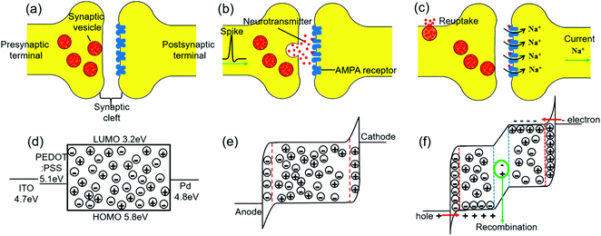 |
| | Fig. 1 Schematic illustration of the mechanisms of a biological synapse (a–c) and an OMIEC memristor (d–f). | |
3.2. Effect of salt concentration on the ion conductivity
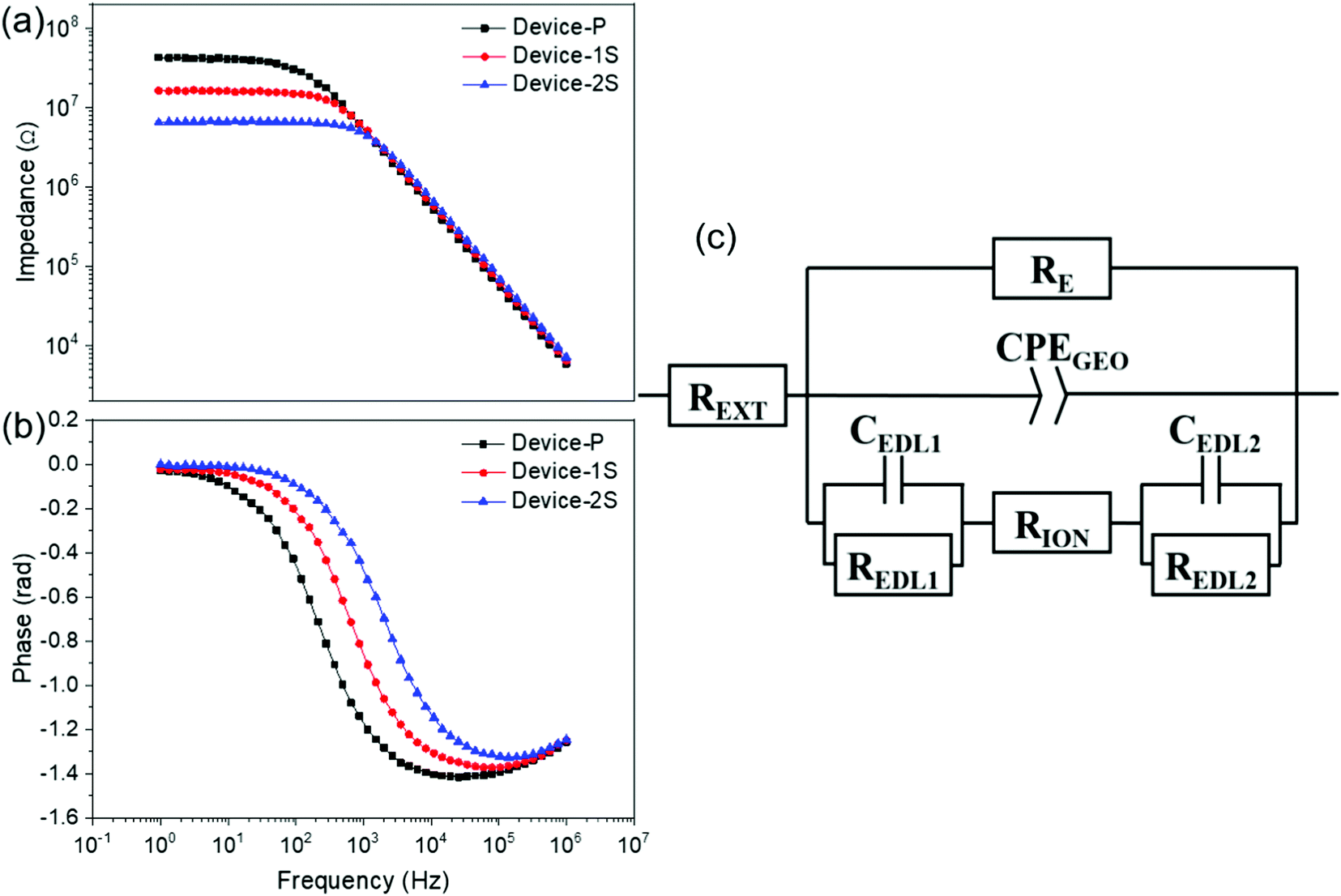
Electrochemical impedance spectroscopy (EIS) was performed to understand how the concentration of the LiClO4 salt affects the trend of ion conductivity in the active layer of the OMIEC memristor. The frequency-dependent impedance and phase spectra of OMIEC memristors are illustrated in Fig. 2. The impedance plateaus in the low-frequency range shown in Fig. 2a indicate a strong correlation with the fraction of the lithium salt additive. Namely, a decreased impedance plateau was observed with an increase in the concentration of LiClO4 from 0 to 2 wt%. The ion conductivity of Device-P depends only on the anions (PF6− ions) because of the negligible Ru(bpy)32+ cation mobility due to their size differences. The low cation conductivity can be compensated by adding Li+ ions that are smaller in size and thus have a higher mobility than the Ru(bpy)32+ ions. Consequently, the device with a higher concentration of the LiClO4 salt showed a decreased impedance plateau as shown in Fig. 2a. A similar trend can be found in previously reported literature36,49,50.
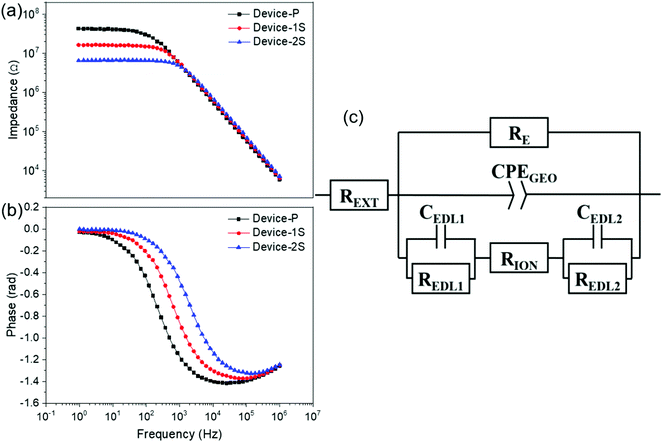 |
| | Fig. 2 EIS curves of Ru(bpy)3(PF6)2 memristor devices with different concentrations of LiClO4. (a) Impedance versus frequency data and (b) phase versus frequency data for Device-P (black squares), Device-1S (red circles), and Device-2S (blue triangles). (c) An equivalent circuit employed for EIS fitting of the OMIEC memristor devices. | |
For additional analysis of the EIS data, an equivalent circuit was employed as shown in Fig. 2c and described in more detail in the ESI.† The spectral data in Fig. 2a and b were fitted to extract typical device parameters from the equivalent circuit (provided in Table S1, ESI†). The decreased bulk ionic resistance (RION) was observed in the device with a higher Li+ concentration, which corroborates the trend of the impedance plateau. The estimated ion conductivities σ in the active layer from the measured resistances are 2.79 × 10⁻¹¹ S cm−1 for Device-P, 7.72 × 10⁻¹¹ S cm−1 for Device-1S, and 1.9 × 10⁻¹⁰ S cm−1 for Device-2S (Table 1).
Table 1 Device parameters for three OMIEC memristors with varying salt concentrations (Device-P, Device-1S, and Device-2S)
| Device |
Active layer |
Ion conductivity, σ (×10−11 S cm−1) |
Turn-on time, τon (s) |
Relaxation time, τre (s) |
PPF index (%) |
PPF relaxation time |
4 + 1 PPF index (%) |
|
τ
1 (ms) |
τ
2 (s) |
| Device-P |
Ru(bpy)3(PF6)2 |
2.79 |
3.8 |
3.5 |
24.2 |
112 |
3.28 |
1.9 |
| Device-1S |
Ru(bpy)3(PF6)2 + 1 wt% of LiClO4 |
7.72 |
1.7 |
1.7 |
44.4 |
96 |
2.14 |
1.4 |
| Device-2S |
Ru(bpy)3(PF6)2 + 2 wt% of LiClO4 |
19.0 |
0.64 |
0.81 |
84.1 |
75 |
1.07 |
2.3 |
3.3. Pinched memristor hysteresis behavior
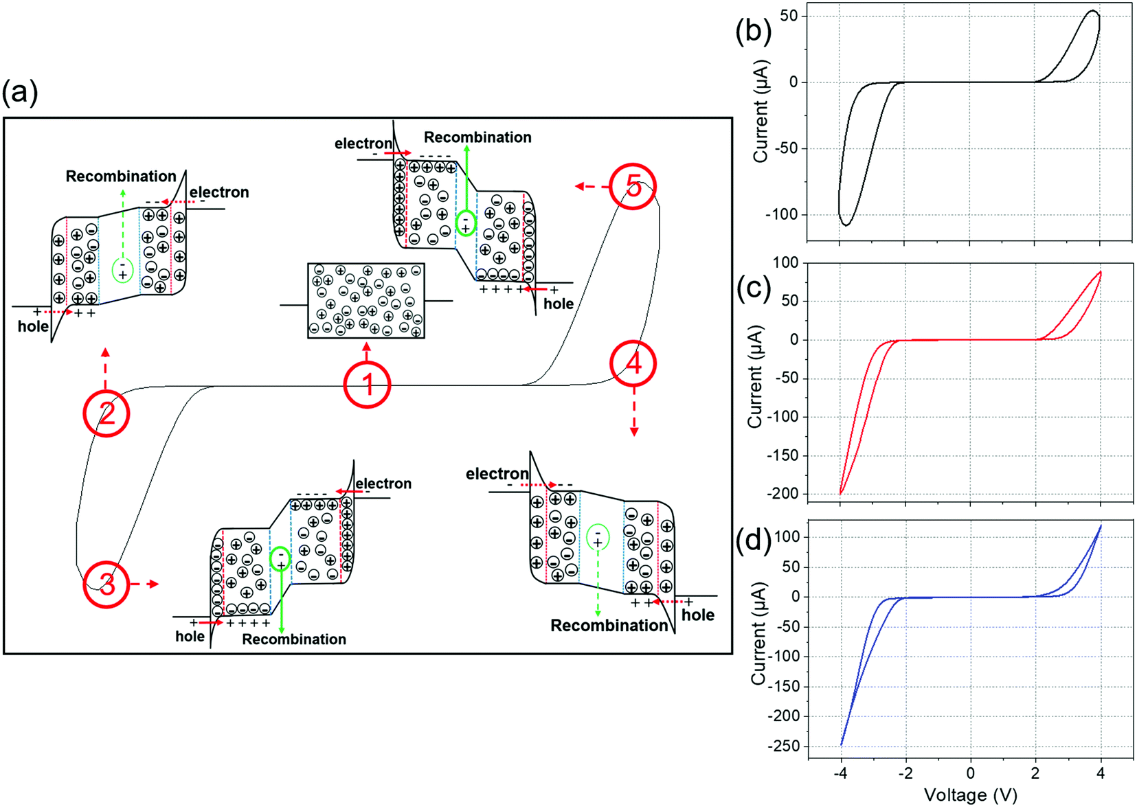
One of the distinctive signatures of the memristor is a hysteresis loop pinched at the I–V origin51. Fig. 3a demonstrates a typical hysteresis loop with the ion distributions of our OMIEC memristive device when the voltage is swept. When a negative voltage is applied to the initial state (step 1) of the device, the ions build up on the electrode surfaces, and then the recombination current starts to flow as shown in step 2. However, it is challenging for electrons and holes to be injected into the active layer owing to the relatively small amount of accumulated ions in step 2. On the other hand, step 3 shows more accumulated ions on the electrode surfaces than step 2, which leads to a sharp increase in the electric field near the interfaces, promoting the injection of electrons and holes. Therefore, the value of recombination current in step 3 is much higher than that in step 2 despite their same applied voltage. It is worth noting that our OMIEC memristive device remembers its most recent resistance through the number of accumulated ions. Also, it can be observed that the accumulated ions on the electrode surfaces diffuse back to their stable state very fast, which is a characteristic of STM. Steps 4 and 5 indicate the same phenomenon as steps 2 and 3 when a positive voltage is applied to the OMIEC memristor.
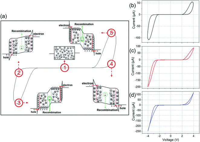 |
| | Fig. 3 (a) A representative current versus voltage curve and the ion distributions of the OMIEC memristor describing each sequential step. The numbers on the curve indicate the initial state at 0 V for step 1 (①), negatively biased states at −3.5 V for step 2 (②) and step 3 (③), and positively biased states at 3.5 V for step 4 (④) and step 5 (⑤). Current–voltage curves of (b) Device-P, (c) Device-1S, and (d) Device-2S. The voltage was swept following the sequence 0 V → −4 V → 0 V → +4 V → 0 V with a scan rate of 0.1 V s−1. | |
Fig. 3b–d shows the hysteresis curves pinched at the origin in the current–voltage (I–V) sweep graphs. The I–V curves of our OMIEC memristors were obtained by sequential direct voltage sweep from 0 V to +4 V and from 0 V to −4 V at a scan rate of 0.1 V s−1. As shown in Fig. 3b–d, a broad shape of hysteresis was obtained for Device-P, while the hysteresis shape is narrower for Device-1S and the narrowest for Device-2S. The device with a higher concentration of additive acquired a narrower shape of the hysteresis because it shows faster ion accumulation and diffusion in the active layer. Fig. S3 (ESI†), which shows the I–V curves in the semi-log scales of devices, demonstrates that the turn-on voltages of the devices are between 2 and 3 V for all three memristive devices.
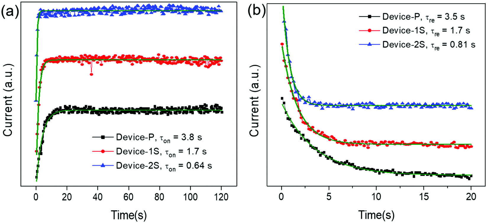
3.4. Turn-on time and relaxation time
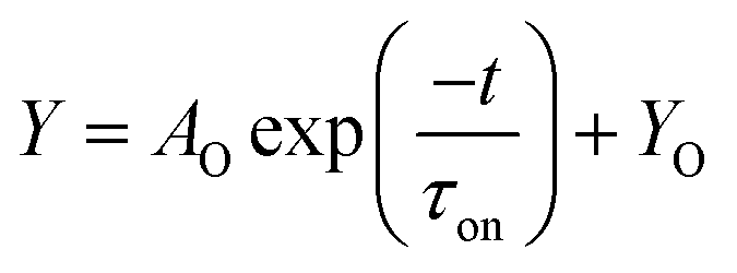
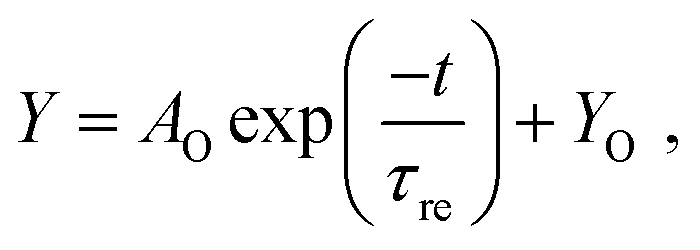
The turn-on time of the OMIEC memristor is the time it takes for ions to accumulate on electrode surfaces and corresponds to the required time for released neurotransmitters to bind with AMPA receptors in the biological synapse. Previous literature demonstrated that the turn-on time of OMIEC devices is related to the average consumption time for crossing half of the two electrodes48,50,52,53. As the variation of the device thickness was minimized during the fabrication process, it is believed that the ion conductivity is a dominant factor to characterize the turn-on time of our OMIEC memristors. Fig. 4a shows the time-dependent current spectra for measuring the turn-on time of our OMIEC devices by applying a constant voltage of 3.5 V on unbiased devices. All three curves, which demonstrate increasing currents from low to saturated values, were fitted to an exponential equation:| | 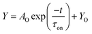 | (1) |
where A0 and Y0 are constants and τon is the turn-on time denoted with green fitting curves in Fig. 4a. The values of the turn-on time are 3.8 s for Device-P, 1.7 s for Device-1S, and 640 ms for Device-2S (Table 1). These data indicate that the device with a higher concentration of the LiClO4 salt has a shorter turn-on time due to its higher ion conductivity. The values of the turn-on time by varying the applied voltage were also measured and are illustrated in Fig. S4 (ESI†). This demonstrates that the turn-on time decreases with increasing biased voltage for all the devices.
 |
| | Fig. 4 Time-dependent current spectra for (a) turn-on time and (b) relaxation time of Device-P (black squares), Device-1S (red circles), and Device-2S (blue triangles) as indicated. The acquired turn-on time and relaxation time data were fitted to eqn (1) and (2), respectively, indicated with solid green lines. | |
On the other hand, the relaxation time is defined as the time it takes for ions accumulated on the electrode surfaces to diffuse back to a stable state54. The relaxation time of the OMIEC memristor can be assumed to be correlated with the duration time of neurotransmitters to be bound with receptors. Fig. 4b shows the time-dependent current spectra to measure the relaxation time of OMIEC devices by applying a read voltage of 1.5 V on the devices turned on in a prior step. Since the biased voltage dropped from 3.5 V to 1.5 V, the current level was also decreased and saturated. The curves were fitted to an exponential equation:
| |  | (2) |
where
A0 and
Y0 are constants and
τre is the relaxation time denoted with green fitting curves in
Fig. 4b. The values of the relaxation time are 3.5 s for Device-P, 1.7 s for Device-1S, and 810 ms for Device-2S (
Table 1). These data indicate that a higher ion conductivity causes a faster relaxation time. For statistical analysis, turn-on and relaxation time measurements were conducted on 10 pristine devices each and their stabilized current values were measured, presented with their average and standard deviation in Tables S2–S5 (ESI
†).
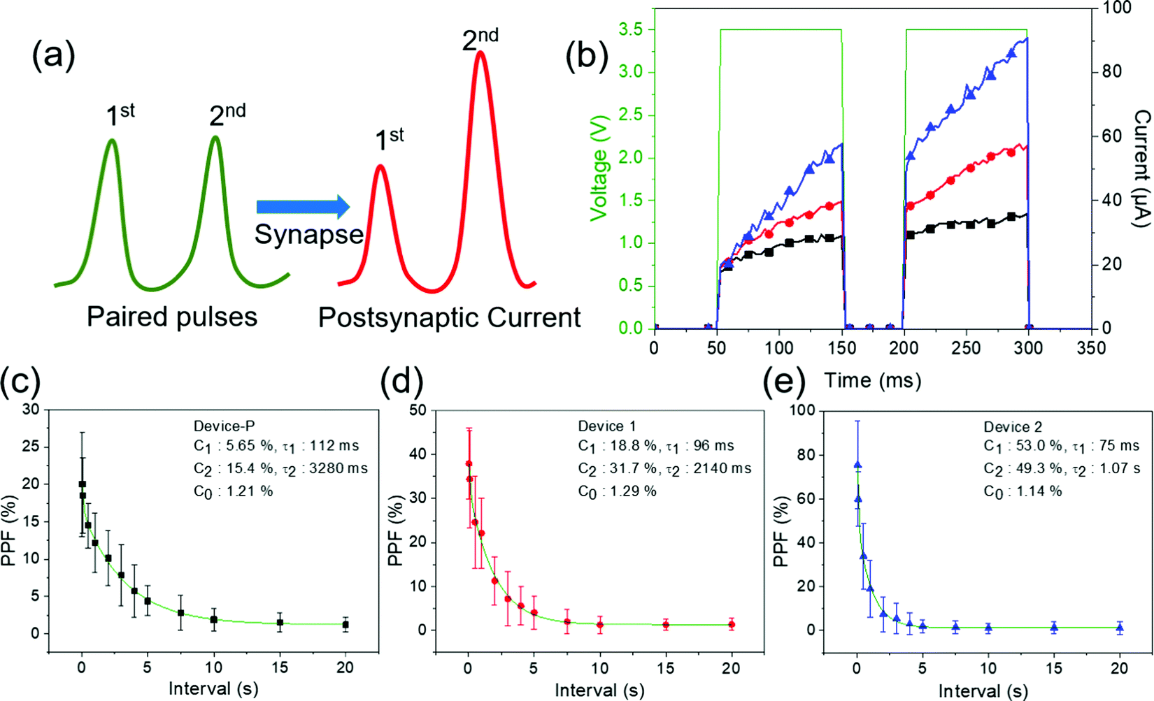
3.5. Paired-pulse facilitation
Fig. 5a illustrates the paired-pulse facilitation (PPF) in a biological synapse. PPF is a phenomenon of the synaptic enhancement to the second pulse when two presynaptic spikes closely follow.55–58 For emulating the presynaptic spikes, two 3.5 V pulses (100 ms in duration and 50 ms in interval time) were applied to the OMIEC memristors as shown in Fig. 5b. For all three memristive devices, the current level of the second spike (I2) is larger than that of the first one (I1), where I1 and I2 are the average values of the measured current data in the range of the duration time. Since the duration time of each spike and the interval time between two pulses are shorter than the turn-on time and relaxation time of the devices, respectively, the conductance was enhanced as shown in Fig. 5b.
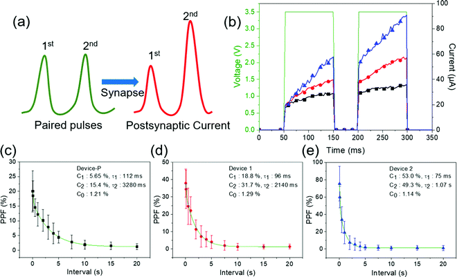 |
| | Fig. 5 (a) Schematic illustration of the PPF phenomenon in a biological synapse between a presynaptic neuron and a postsynaptic neuron. (b) Two 3.5 V applied pulses (100 ms in duration and 50 ms in interval time) and the consequent current are depicted for Device-P (black squares), Device-1S (red circles), and Device-2S (blue triangles). PPF data and their statistical distribution as a function of the pulse interval with a fixed pulse magnitude and duration at 3.5 V and 100 ms, respectively, for (c) Device-P (black squares), (d) Device-1S (red circles), and (e) Device-2S (blue triangles). The measured PPF data were fitted with eqn (3) and are indicated with green curves. The acquired parameters by fitting are demonstrated in the inset of each graph. | |
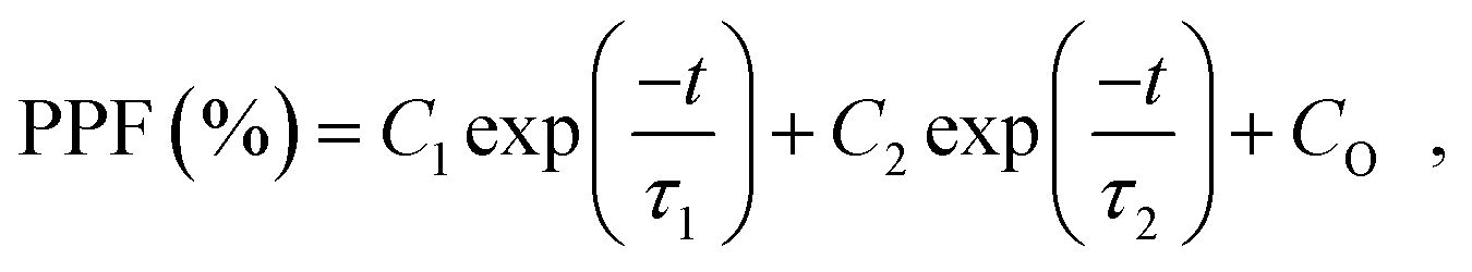
The PPF index, i.e. (I2 − I1)/I1 × 100%, is largely affected by the concentration of the LiClO4 additive. Its values are 24.2%, 44.4%, and 84.1% for Device-P, Device-1S, and Device-2S, respectively, which are summarized in Table 1. These different values of the PPF index can be explained by ion conductivity. Device-2S shows a larger PPF index because the current level increased more than that in the case of Device-P or Device-1S during the same 100 ms, which contributed to its high ion conductivity. Fig. 5c–e presents the PPF data and their statistical distribution as a function of the interval time. Here, the pulse magnitude and duration were fixed at 3.5 V and 100 ms, respectively, and the pulse interval was increased from 50 ms to 20 s. The relationship between the PPF and interval time was fitted by the equation:
| |  | (3) |
where
C0,
C1, and
C2 are constants and
τ1 and
τ2 are the PPF relaxation times denoted with the green fitting curves in
Fig. 5c–e. In our fitting results, the values of
τ1 = 112 ms and
τ2 = 3.28 s for Device-P,
τ1 = 96 ms and
τ2 = 2.14 s for Device-1S, and
τ1 = 75 ms and
τ2 = 1.07 s for Device-2S were calculated (
Table 1). In the biological synapse, the timescales of two phases (
τ1 and
τ2) are tens of milliseconds and hundreds of milliseconds
59. Therefore, the fitting results of Device-2S showed a closer PPF relaxation time to biological synapses compared with Device-P or Device-1S.
Fig. S5 (ESI†) indicates the PPF as a function of pulse magnitude (ranging from 3 to 4.5 V) with a fixed 50 ms interval time and a 100 ms pulse duration time. Also, the pulse duration time (ranging from 50 to 300 ms) dependent PPF data are shown in Fig. S6 with a fixed 50 ms interval time and a 3.5 V pulse magnitude. These data demonstrated that the average PPF increases with increasing pulse magnitude or pulse duration.
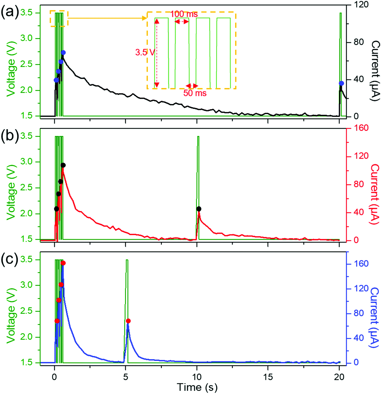
3.6. Short-term synaptic plasticity
The dynamic change of a synapse, which decays back to its normal state within hundreds of milliseconds to a few seconds, is termed short-term synaptic plasticity (STP) in biological synapses45. The STP in biology can be measured by activating 4 presynaptic spikes sequentially and a fifth spike after a few seconds, observing the recovery of the conductance level. To emulate the STP properties, the current changes of our OMIEC memristors were measured while applying 4 + 1 spikes, as depicted in Fig. 6. During the 4 presynaptic spikes (3.5 V of pulse magnitude, 100 ms in duration, and 50 ms in interval time), the current was enhanced following the PPF index, which means that the current level of Device-2S increased more than that of Device-P or Device-1S. After the fourth spike, the current decay rate of each device was affected by its relaxation time constant, i.e. the pristine device takes a longer time to recover its initial state than the device with a higher concentration of the additive salt. The recovery timescale of Device-2S is similar to that of a biological synapse. The PPF indices between the first and fifth spikes, i.e. (I5 − I1)/I1 × 100%, are 1.9% for Device-P, 1.4% for Device-1S, and 2.3% for Device-2S, which indicate that the current levels of the devices recovered after enough decay time (Table 1). Therefore, our OMIEC devices can be described as memristors that have STM properties.
 |
| | Fig. 6 Emulating the short-term synaptic plasticity. The current change was measured while applying 4 + 1 presynaptic spikes on (a) Device-P, (b) Device-1S, and (c) Device-2S. | |
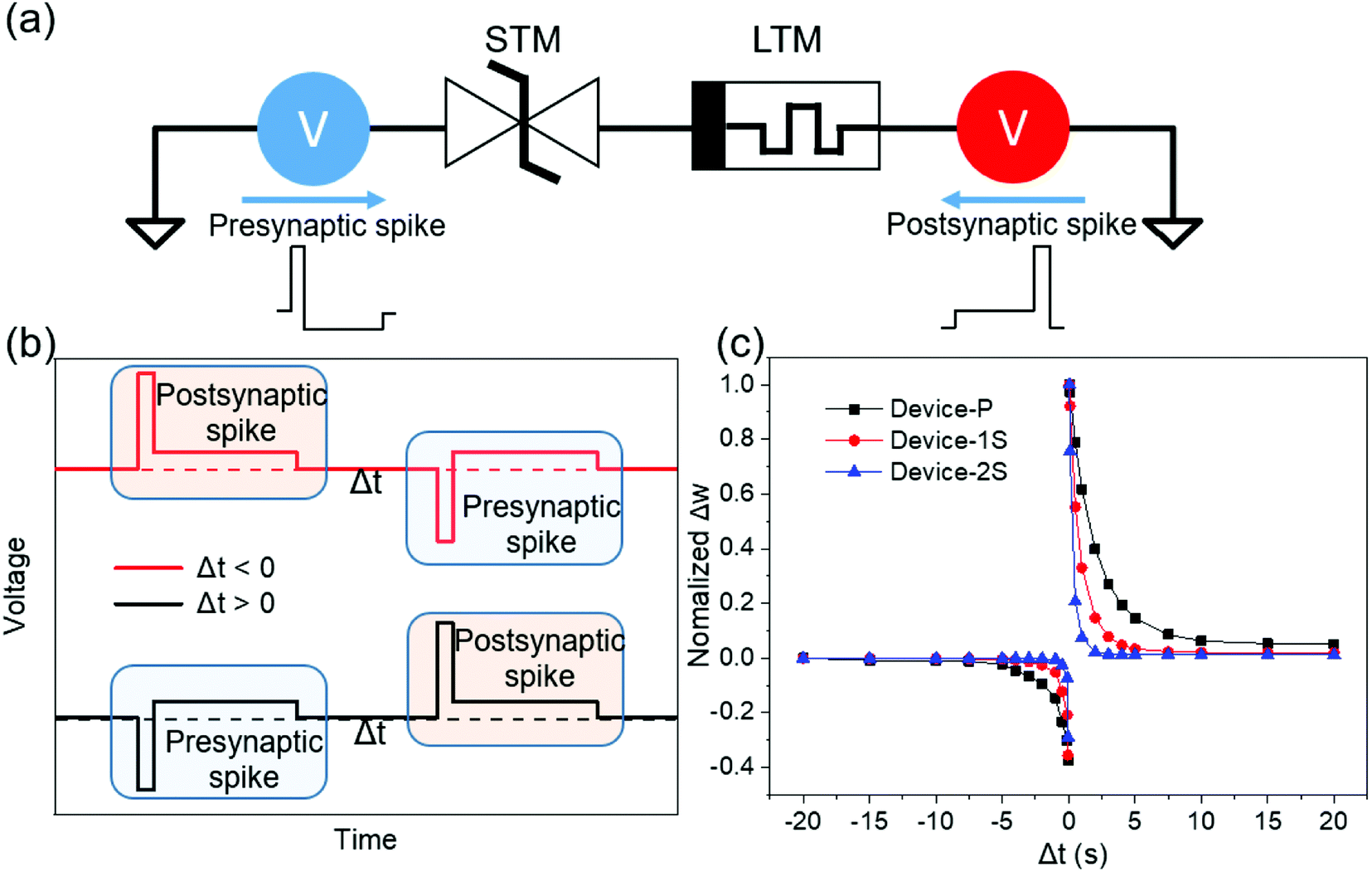
3.7. Modulation of STDP learning curves
Fig. 7a shows a series circuit to conduct a simulation for implementing the STDP learning rule27. In this SPICE simulation, our OMIEC devices were employed as STM synaptic devices because they can emulate the neurotransmitter dynamics in the presynaptic terminal of a biological synapse, which causes the OMIEC memristor to modulate the STDP of the LTM synaptic device. Fig. 7b illustrates two consecutive pulses applied to the series circuit. The first and second pulses are a presynaptic spike and a postsynaptic spike, respectively, and they are separated by the time difference (Δt).27 Each spike consists of a short pulse that can control the resistance of the LTM and a long pulse that turns on the STM. Fig. 7c shows the normalized weight change versus time difference curves, and they are fitted by an STDP equation:60| | 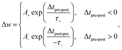 | (4) |
where Δw is a weight change, A+ and A− are the fitting parameters, and Δtpre-post and Δtpost-pre are the time intervals between the presynaptic and postsynaptic spikes. Although there are two time constants (τ+ and τ−) in the equation, they can be unified as a STDP time constant (τSTDP) because the absolute values of the two parameters are almost identical.
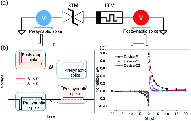 |
| | Fig. 7 (a) A series circuit for the STDP simulation, (b) presynaptic and postsynaptic spikes, applied pulse on a series circuit; short pulse: 14 V (pre) and 18 V (post) with 500 μs, long pulse: 6 V with 200 ms, Δt: 50 ms–20 s, and (c) normalized weight change versus time difference for OMIEC devices. | |
In this simulation, the OMIEC device acts as a voltage divider, allowing STDP learning without pulse generator synchronization or pulse overlap as previously reported in the literature. Also, the OMIEC device can control the value of τSTDP easily by tuning its ion conductivity. The value of τSTDP decreases by increasing the salt concentration, which is similar to the PPF fitting result. The used models, ECM data, simulation operation, and fitting results are described in the ESI† (Fig. S7–S10).
4. Conclusions
In this study, we demonstrated a new OMIEC memristor using Ru(bpy)3(PF6)2 as an active layer that emulates the short-term characteristics of a biological synapse. Besides, the performances of the memristors can be tuned by adding the LiClO4 salt, which affects the ion conductivity of the active layer. EIS was performed to measure the ion conductivities of the devices. Also, the I–V characteristics, turn-on time, relaxation time, and PPF indices of OMIEC memristors were measured to explain their correlation with biological synaptic properties. Additionally, short-term synaptic plasticity was mimicked by applying 4 + 1 spikes and the current was measured to verify the STM characteristics of our memristive devices. The above data confirmed that Device-2S, which consisted of Ru(bpy)3(PF6)2 with 2% LiClO4, showed similar timescales to the STP characteristics of biological synapses. Lastly, the SPICE simulation shows a tunable STDP time constant by connecting our OMIEC memristor, which can mimic the calcium ion dynamics in a biological synapse, to the LTM synaptic device. These results make our OMIEC memristor a good candidate for the neuromorphic device, paving the way to implement electronic synapses in future applications.
Conflicts of interest
The authors declare that they have no conflicts of interest.
Acknowledgements
This work was supported by Korea Institute of Science and Technology (Grant No. 2E31031 and 2E31041) and the National Research Foundation of Korea (NRF) (NRF-2019M3F3A1A02072175 and NRF-2021M3F3A2A01037738).
References
- J. von Neumann, First draft of a report on the EDVAC, IEEE Ann. Hist. Comput., 1993, 15, 27–75, DOI:10.1109/85.238389.
- H. G. Cragon, Computer architecture and implementation, Meas. Sci. Technol., 2001, 12, 1744–1745, DOI:10.1088/0957-0233/12/10/704.
- J. Fan, F. Han and H. Liu, Challenges of big data analysis, Natl. Sci. Rev., 2014, 1, 293–314, DOI:10.1093/nsr/nwt032.
- Z. Allam and Z. A. Dhunny, On big data, artificial intelligence and smart cities, Cities, 2019, 89, 80–91, DOI:10.1016/j.cities.2019.01.032.
- C. Mead, Neuromorphic electronic systems, Proc. IEEE, 1990, 78, 1629–1636, DOI:10.1109/5.58356.
- L. F. Abbott and W. G. Regehr, Synaptic computation, Nature, 2004, 431, 796–803, DOI:10.1038/nature03010.
- G. Indiveri, B. Linares-Barranco, T. J. Hamilton, A. van Schaik, R. Etienne-Cummings, T. Delbruck, S.-C. Liu, P. Dudek, P. Häfliger, S. Renaud, J. Schemmel, G. Cauwenberghs, J. Arthur, K. Hynna, F. Folowosele, S. Saïghi, T. Serrano-Gotarredona, J. Wijekoon, Y. Wang and K. Boahen, Neuromorphic silicon neuron circuits, Front. Neurosci., 2011, 5, 1–23, DOI:10.3389/fnins.2011.00073.
- A. R. Young, M. E. Dean, J. S. Plank and G. S. Rose, A review of spiking neuromorphic hardware communication systems, IEEE Access, 2019, 7, 135606–135620, DOI:10.1109/ACCESS.2019.2941772.
- B. V. Benjamin, P. Gao, E. McQuinn, S. Choudhary, A. R. Chandrasekaran, J. Bussat, R. Alvarez-Icaza, J. V. Arthur, P. A. Merolla and K. Boahen, Neurogrid: A mixed-analog-digital multichip system for large-scale neural simulations, Proc. IEEE, 2014, 102, 699–716, DOI:10.1109/JPROC.2014.2313565.
- K. Meier, A mixed-signal universal neuromorphic computing system, 2015 IEEE Int. Electron Devices Meet. IEDM, 2015, pp. 4, DOI:10.1109/IEDM.2015.7409627.
- TrueNorth: Design and Tool Flow of a 65 mW 1 Million Neuron Programmable Neurosynaptic Chip – IEEE Journals & Magazine, (n.d.), https://ieeexplore.ieee.org/abstract/document/7229264 (accessed January 15, 2021).
- S. B. Furber, F. Galluppi, S. Temple and L. A. Plana, The SpiNNaker project, Proc. IEEE, 2014, 102, 652–665, DOI:10.1109/JPROC.2014.2304638.
- M. Davies, N. Srinivasa, T. Lin, G. Chinya, Y. Cao, S. H. Choday, G. Dimou, P. Joshi, N. Imam, S. Jain, Y. Liao, C. Lin, A. Lines, R. Liu, D. Mathaikutty, S. McCoy, A. Paul, J. Tse, G. Venkataramanan, Y. Weng, A. Wild, Y. Yang and H. Wang, Loihi: A neuromorphic manycore processor with on-chip learning, IEEE Micro, 2018, 38, 82–99, DOI:10.1109/MM.2018.112130359.
- RRAM-based synapse for neuromorphic system with pattern recognition function – IEEE Conference Publication, (n.d.). https://ieeexplore.ieee.org/document/6479016 (accessed January 15, 2021).
-
D. S. Jeong, Hardware spiking artificial neurons, their response function, and noises, in Adv. Neuromorphic Hardw. Exploit. Emerg. Nanoscale Devices, ed. M. Suri, Springer India, New Delhi, 2017, pp. 1–16 DOI:10.1007/978-81-322-3703-7_1.
- L. Chua, Memristor – The missing circuit element, IEEE Trans. Circuit Theory, 1971, 18, 507–519, DOI:10.1109/TCT.1971.1083337.
- J. J. Yang, D. B. Strukov and D. R. Stewart, Memristive devices for computing, Nat. Nanotechnol., 2013, 8, 13–24, DOI:10.1038/nnano.2012.240.
-
R. Waser and M. Aono, Nanoionics-based resistive switching memories, in Nanosci. Technol., Co-Published with Macmillan Publishers Ltd, UK, 2009, pp. 158–165 DOI:10.1142/9789814287005_0016.
- S. H. Jo, T. Chang, I. Ebong, B. B. Bhadviya, P. Mazumder and W. Lu, Nanoscale memristor device as synapse in neuromorphic systems, Nano Lett., 2010, 10, 1297–1301, DOI:10.1021/nl904092h.
- K. Kim, S. Park, S. M. Hu, J. Song, W. Lim, Y. Jeong, J. Kim, S. Lee, J. Y. Kwak, J. Park, J. K. Park, B.-K. Ju, D. S. Jeong and I. Kim, Enhanced analog synaptic behavior of SiN x/a-Si bilayer memristors through Ge implantation, NPG Asia Mater., 2020, 12, 1–13, DOI:10.1038/s41427-020-00261-0.
- Z. Wang, M. Yin, T. Zhang, Y. Cai, Y. Wang, Y. Yang and R. Huang, Engineering incremental resistive switching in TaOx based memristors for brain-inspired computing, Nanoscale, 2016, 8, 14015–14022, 10.1039/C6NR00476H.
- W. Banerjee, Q. Liu, H. Lv, S. Long and M. Liu, Electronic imitation of behavioral and psychological synaptic activities using TiOx/Al2O3-based memristor devices, Nanoscale, 2017, 9, 14442–14450, 10.1039/C7NR04741J.
- S. Yu, Y. Wu, R. Jeyasingh, D. Kuzum and H.-S. P. Wong, An electronic synapse device based on metal oxide resistive switching memory for neuromorphic computation, IEEE Trans. Electron Devices, 2011, 58, 2729–2737, DOI:10.1109/TED.2011.2147791.
- R. Berdan, E. Vasilaki, A. Khiat, G. Indiveri, A. Serb and T. Prodromakis, Emulating short-term synaptic dynamics with memristive devices, Sci. Rep., 2016, 6, 1–9, DOI:10.1038/srep18639.
- C. Du, F. Cai, M. A. Zidan, W. Ma, S. H. Lee and W. D. Lu, Reservoir computing using dynamic memristors for temporal information processing, Nat. Commun., 2017, 8, 2204, DOI:10.1038/s41467-017-02337-y.
- G. Srinivasan, A. Sengupta and K. Roy, Magnetic tunnel junction based long-term short-term stochastic synapse for a spiking neural network with on-chip STDP learning, Sci. Rep., 2016, 6, 29545, DOI:10.1038/srep29545.
- Z. Wang, S. Joshi, S. E. Savel’ev, H. Jiang, R. Midya, P. Lin, M. Hu, N. Ge, J. P. Strachan, Z. Li, Q. Wu, M. Barnell, G.-L. Li, H. L. Xin, R. S. Williams, Q. Xia and J. J. Yang, Memristors with diffusive dynamics as synaptic emulators for neuromorphic computing, Nat. Mater., 2017, 16, 101–108, DOI:10.1038/nmat4756.
- Y. Sun, H. Xu, S. Liu, B. Song, H. Liu, Q. Liu and Q. Li, Short-term and long-term plasticity mimicked in low-voltage Ag/GeSe/TiN electronic synapse, IEEE Electron Device Lett., 2018, 39, 492–495, DOI:10.1109/LED.2018.2809784.
- B. D. Paulsen, K. Tybrandt, E. Stavrinidou and J. Rivnay, Organic mixed ionic–electronic conductors, Nat. Mater., 2020, 19, 13–26, DOI:10.1038/s41563-019-0435-z.
- D. Moia, A. Giovannitti, A. A. Szumska, I. P. Maria, E. Rezasoltani, M. Sachs, M. Schnurr, P. R. F. Barnes, I. McCulloch and J. Nelson, Design and evaluation of conjugated polymers with polar side chains as electrode materials for electrochemical energy storage in aqueous electrolytes, Energy Environ. Sci., 2019, 12, 1349–1357, 10.1039/C8EE03518K.
- Y. Cao, G. Yu, A. J. Heeger and C. Y. Yang, Efficient, fast response light-emitting electrochemical cells: Electroluminescent and solid electrolyte polymers with interpenetrating network morphology, Appl. Phys. Lett., 1996, 68, 3218–3220, DOI:10.1063/1.116442.
- S. Inal, J. Rivnay, P. Leleux, M. Ferro, M. Ramuz, J. C. Brendel, M. M. Schmidt, M. Thelakkat and G. G. Malliaras, A high transconductance accumulation mode electrochemical transistor, Adv. Mater., 2014, 26, 7450–7455, DOI:10.1002/adma.201403150.
- J. Jang, J. Ha and J. Cho, Fabrication of water-dispersible polyaniline-poly(4-styrenesulfonate) nanoparticles for inkjet-printed chemical-sensor applications, Adv. Mater., 2007, 19, 1772–1775, DOI:10.1002/adma.200602127.
- C.-C. Shih, C.-W. Huang, M. Gao, C.-C. Chueh and W.-C. Chen, Multi-state memristive behavior in a light-emitting electrochemical cell, J. Mater. Chem. C, 2017, 5, 11421–11428, 10.1039/C7TC03920D.
- Y. van de Burgt, E. Lubberman, E. J. Fuller, S. T. Keene, G. C. Faria, S. Agarwal, M. J. Marinella, A. Alec Talin and A. Salleo, A non-volatile organic electrochemical device as a low-voltage artificial synapse for neuromorphic computing, Nat. Mater., 2017, 16, 414–418, DOI:10.1038/nmat4856.
- H. Rudmann, S. Shimada and M. F. Rubner, Solid-state light-emitting devices based on the tris-chelated ruthenium(II) complex. 4. High-efficiency light-emitting devices based on derivatives of the tris(2,2′-bipyridyl) ruthenium(II) complex, J. Am. Chem. Soc., 2002, 124, 4918–4921, DOI:10.1021/ja012721j.
- H. Rudmann and M. F. Rubner, Single layer light-emitting devices with high efficiency and long lifetime based on tris(2,2′-bipyridyl) ruthenium(II) hexafluorophosphate, J. Appl. Phys., 2001, 90, 4338–4345, DOI:10.1063/1.1409577.
- M. Buda, G. Kalyuzhny and A. J. Bard, Thin-film solid-state electroluminescent devices based on tris(2,2′-bipyridine)ruthenium(II) complexes, J. Am. Chem. Soc., 2002, 124, 6090–6098, DOI:10.1021/ja017834h.
- H. Rudmann, S. Shimada and M. F. Rubner, Operational mechanism of light-emitting devices based on Ru(II) complexes: Evidence for electrochemical junction formation, J. Appl. Phys., 2003, 94, 115–122, DOI:10.1063/1.1578174.
- J. Slinker, D. Bernards, P. L. Houston, H. D. Abruña, S. Bernhard and G. G. Malliaras, Solid-state electroluminescent devices based on transition metal complexes, Chem. Commun., 2003, 2392–2399, 10.1039/B304265K.
- J. D. Slinker, J. Rivnay, J. S. Moskowitz, J. B. Parker, S. Bernhard, H. D. Abruña and G. G. Malliaras, Electroluminescent devices from ionic transition metal complexes, J. Mater. Chem., 2007, 17, 2976–2988, 10.1039/B704017B.
- R. Berdan, C. Lim, A. Khiat, C. Papavassiliou and T. Prodromakis, A memristor SPICE model accounting for volatile characteristics of practical ReRAM, IEEE Electron Device Lett., 2014, 35, 135–137, DOI:10.1109/LED.2013.2291158.
- C. Yakopcic, T. M. Taha, G. Subramanyam, R. E. Pino and S. Rogers, A memristor device model, IEEE Electron Device Lett., 2011, 32, 1436–1438, DOI:10.1109/LED.2011.2163292.
- M. H. Maruf and S. I. Ali, Review and comparative study of I–V characteristics of different memristor models with sinusoidal input, Int. J. Electron., 2020, 107, 349–375, DOI:10.1080/00207217.2019.1661021.
-
W. Gerstner, W. M. Kistler, R. Naud and L. Paninski, Neuronal Dynamics: From Single Neurons to Networks and Models of Cognition, Cambridge University Press, 2014 Search PubMed.
- R. D. Costa, E. Ortí, H. J. Bolink, F. Monti, G. Accorsi and N. Armaroli, Luminescent ionic transition-metal complexes for light-emitting electrochemical cells, Angew. Chem.,
Int. Ed., 2012, 51, 8178–8211, DOI:10.1002/anie.201201471.
-
M. Bear, B. Connors and M. A. Paradiso, Neuroscience: Exploring the Brain, Enhanced Edition, Jones & Bartlett Learning, 2020 Search PubMed.
- S. B. Meier, D. Tordera, A. Pertegás, C. Roldán-Carmona, E. Ortí and H. J. Bolink, Light-emitting electrochemical cells: Recent progress and future prospects, Mater. Today, 2014, 17, 217–223, DOI:10.1016/j.mattod.2014.04.029.
- Y. Hu and J. Gao, Cationic effects in polymer light-emitting electrochemical cells, Appl. Phys. Lett., 2006, 89, 253514, DOI:10.1063/1.2422877.
- Y. Shen, D. D. Kuddes, C. A. Naquin, T. W. Hesterberg, C. Kusmierz, B. J. Holliday and J. D. Slinker, Improving light-emitting electrochemical cells with ionic additives, Appl. Phys. Lett., 2013, 102, 203305, DOI:10.1063/1.4807674.
- Y. V. Pershin and M. D. Ventra, Memory effects in complex materials and nanoscale systems, Adv. Phys., 2011, 60, 145–227, DOI:10.1080/00018732.2010.544961.
- S. van Reenen, R. A. J. Janssen and M. Kemerink, Dynamic processes in sandwich polymer light-emitting electrochemical cells, Adv. Funct. Mater., 2012, 22, 4547–4556, DOI:10.1002/adfm.201200880.
- F. G. Gao and A. L. Bard, Solid-state organic light-emitting diodes based on tris(2,2′-bipyridine)ruthenium(II) complexes, J. Am. Chem. Soc., 2000, 30, 7426–7427, DOI:10.1021/ja000666t.
-
Y. Halawani, B. Mohammad, D. Homouz, M. Al-Qutayri and H. Saleh, Embedded memory design using memristor: Retention time versus write energy, in 2013 IEEE 20th Int. Conf. Electron. Circuits Syst. ICECS, 2013, pp. 41–44 DOI:10.1109/ICECS.2013.6815340.
- S. G. Hu, Y. Liu, T. P. Chen, Z. Liu, Q. Yu, L. J. Deng, Y. Yin and S. Hosaka, Emulating the paired-pulse facilitation of a biological synapse with a NiOx-based memristor, Appl. Phys. Lett., 2013, 102, 183510, DOI:10.1063/1.4804374.
- D. W. Kim, J. C. Yang, S. Lee and S. Park, Neuromorphic processing of pressure signal using integrated sensor-synaptic device capable of selective and reversible short- and long-term plasticity operation, ACS Appl. Mater. Interfaces, 2020, 12, 23207–23216, DOI:10.1021/acsami.0c03904.
- R. Yu, E. Li, X. Wu, Y. Yan, W. He, L. He, J. Chen, H. Chen and T. Guo, Electret-based organic synaptic transistor for neuromorphic computing, ACS Appl. Mater. Interfaces, 2020, 12, 15446–15455, DOI:10.1021/acsami.9b22925.
- Q. Liu, Y. Liu, J. Li, C. Lau, F. Wu, A. Zhang, Z. Li, M. Chen, H. Fu, J. Draper, X. Cao and C. Zhou, Fully printed all-solid-state organic flexible artificial synapse for neuromorphic computing, ACS Appl. Mater. Interfaces, 2019, 11, 16749–16757, DOI:10.1021/acsami.9b00226.
- R. S. Zucker and W. G. Regehr, Short-term synaptic plasticity, Annu. Rev. Physiol., 2002, 64, 355–405, DOI:10.1146/annurev.physiol.64.092501.114547.
- J. Jiang, W. Hu, D. Xie, J. Yang, J. He, Y. Gao and Q. Wan, 2D electric-double-layer phototransistor for photoelectronic and spatiotemporal hybrid neuromorphic integration, Nanoscale, 2019, 11, 1360–1369, 10.1039/C8NR07133K.
Footnote |
| † Electronic supplementary information (ESI) available. See DOI: 10.1039/d1ma01078f |
|
| This journal is © The Royal Society of Chemistry 2022 |
Click here to see how this site uses Cookies. View our privacy policy here. 
 Open Access Article
 This Open Access Article is licensed under a Creative Commons Attribution-Non Commercial 3.0 Unported Licence
 a,
Jaewook
Kim
a,
Suyoun
Lee
a,
Jaewook
Kim
a,
Suyoun
Lee