
 Open Access Article
 This Open Access Article is licensed under a
 Creative Commons Attribution 3.0 Unported Licence
Introducing neat fullerenes to improve the thermal stability of slot-die coated organic solar cells†
Bradley
Kirk
,
Xun
Pan
,
Martyn
Jevric
,
Gunther
Andersson
 and
Mats R.
Andersson
*
and
Mats R.
Andersson
*
Flinders Institute for Nanoscale Science and Technology, Flinders University, Sturt Road, Bedford Park, Adelaide, SA 5042, Australia. E-mail: mats.andersson@flinders.edu.au
First published on 17th February 2022
Abstract
For organic photovoltaics (OPVs) to be considered commercially viable, the devices should not only achieve high performances, but also have relatively long lifespans. In fact, a major source of lifespan reduction is associated with the “burn-in process”, resulting in a sharp initial reduction in performance. PPDT2FBT:PC71BM and PPDT2FT:PC61BM both represent highly robust and efficient cells when fabricated under ambient conditions via slot-die coating and have been shown to be tolerant to elevated temperatures. With accelerated thermal aging at 120 °C, such devices were found to be affected by the burn-in process, greatly diminishing their efficiency. The addition of pristine C70, to the PPDT2FBT:PC61BM bulk-heterojunction (BHJ) was found to improve the thermal stability of slot-die coated OPVs at high temperatures while the addition of C60 speeds up the burn-in process. Initially, the ink preparation for the active layer and fabrication conditions for slot-die coating were optimised to improve the flexible device performance for PPDT2FBT:PC71BM and PPDT2FBT:PC61BM cells, reaching a power conversion efficiency (PCE) of 8.49% and 7.63%, respectively. A subsequent investigation into the thermal stability of PPDT2FBT:PC61BM devices at 85 °C found no significant burn-in process that reduces device performance, which was evidenced at 120 °C, but a continuous degradation process that slowly reduces the device performance. We have found that the addition of 5.0% w/w of C70 (with respect to PCBM) into the active layer blend suppressed the thermal degradation at 120 °C, compared to the binary blend. Dynamic mechanical thermal analysis (DMTA) measurements on the bulk-heterojunction blends further revealed that the thermal behaviour is significantly changed after the addition of small amounts of C70. When compared with the addition of neat C60, a known nucleating agent, the addition of C70 instead appeared to inhibit crystal formation and growth, rather than induce the formation of many smaller crystals. We anticipate that this improved formulation will improve the device lifetimes significantly at lower temperatures.
1. Introduction
Organic photovoltaics (OPVs) have seen increased interest over the past decade owing to their potential to be fabricated as flexible devices, roll-to-roll processability and relatively low fabrication cost.1–3 Since the early developmental stages of OPVs, fullerenes have been the most widely used acceptor materials, especially PC61BM, due to the material's relatively low production cost.4 To enhance the absorption of visible light and increase the power conversion efficiency, PC71BM was also introduced early in the development of OPVs.5 Recently there has been a significant increase in record power conversion efficiencies (PCEs), exceeding 18% for single junction devices.6–8 This is mainly due to the development of strongly absorbing acceptor molecules, however, these molecules are normally produced via multi-step synthesis and are therefore quite expensive to produce. The development of efficient small-scale laboratory fabricated devices has prompted a shift towards large-scale devices which could potentially be used for commercial purposes. In order to fulfill this vision, several coating techniques, including slot-die,9–11 blade,12,13 screen14–16 and spray coating,17–19 are currently being investigated to reduce the performance gap between small and large area devices. The advantage of these techniques over small-scale spin-coated devices is the relatively low material wastage and feasibility of upscaling (>1 m2) fabrication of flexible devices. Recently, there has been increased interest in these materials for their potential usage as indoor solar cells.20Though performance is an important aspect of OPV development, material/fabrication cost and stability are areas that are not as extensively investigated when it comes to large-area devices. For OPV technologies to be competitive with other types of photovoltaic devices, they need to be relatively inexpensive to manufacture and have a comparable lifespan (at least 10 years).21 There are several mechanisms of degradation that have been identified to have significant influence on the lifetime of OPVs. These include thermal,22,23 oxygen and moisture,24,25 UV radiance26,27 and mechanical9,28,29 degradation. These factors are responsible for two significant decay trends of PCE: burn-in and linear degradation.30–32 For burn-in, the performance drop is relatively quick and is usually where the largest decrease in performance occurs, however, the impact of this degradation decreases as time progresses.32–34 After the burn-in, a linear degradation occurs, resulting in a relatively low rate of decay in PCE. It has been shown that the origin behind severe burn-in losses in many systems depends on morphological changes in the active material.33–35
The continuous illumination of the sun can result in an increase in the working temperature of the OPV in outdoor fixtures. It is known that polymers have structural mobility, especially if the environmental temperature exceeds their glass transition temperatures.36,37 This can result in a change of morphology, such as degree of phase separation, over time, for donor–acceptor blends. In the case of polymer:fullerene composites, the thermal energy can lead to the crystallization of the polymer and fullerene components, which leads to a decreased performance.38,39 The formation of large crystals when exposed to heat can lead to a reduction in performance as inefficient exciton dissociation can occur and charge transfer decreases as a result from decrease of the donor/acceptor interfaces. To address fullerene crystallization, one reported method mentioned using nucleating agents to limit the size of fullerene crystallites in the active layer, thus improving the thermal stability.40,41 Lindqvist et al. demonstrated that the addition of as little 2% w/w C60 improved the thermal stability of TQ1:PC61BM based OPVs, even when heated up to 130 °C, which is above the glass transition temperature of this particular bulk-heterojunction (BHJ).42
There are several active materials that have been shown to reach high performances, with some reaching beyond 18% for single junction OPVs.6–8 However, most of these high performing materials were only fabricated into small-scale cells using rigid glass substrate, and the deposition process was protected by nitrogen, which is not easily applicable to large-scale printing/coating method. As of 2021, the highest efficiency to be achieved for large area (≥1 cm2) OPVs has been 12.6%.43 In addition, these high performing materials are also known to have complex synthesis and require many purification steps that make them expensive to upscale and thus, less desirable to use in the fabrication of large-area OPVs.44,45 As seen in Table S1 in ESI,† the high performing materials (PM6, ITIC & Y6) are far more expensive than more maturely developed materials (C60, PC61BM, PC71BM, P3HT).
Poly[(2,5-bis(2hexyldecyloxy)phenylene)-alt-(5,6-difluoro-4,7-di(thiophen-2-yl)benzo[c][1,2,5]thiadiazole)]:[6,6]-phenyl-C61-butyric acid ester (PPDT2FBT:PC61BM) is a promising material combination that can be used as the donor:acceptor material in slot-die coated devices (Fig. 1a). These organic materials have been used to fabricate devices via slot-die coating (rigid46 & flexible47 substrates) with minimal performance losses upon upscaling. In addition, these materials are relatively in-expensive and the synthesis is scalable.48 Lastly, there is a relatively small gap between spin-coated and slot-die coated PPDT2FBT:PC71BM devices, with efficiencies reaching up to 9.39%49 and 7.61%47 respectively.
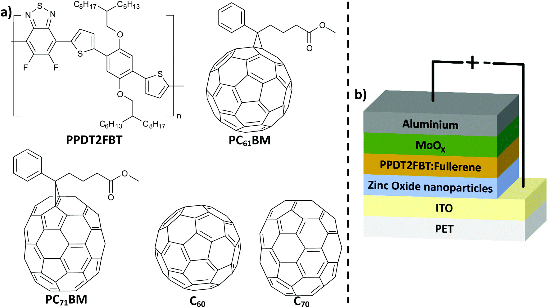 | ||
| Fig. 1 (a) Chemical structure of PPDT2FBT, C60, C70, PC61BM and PC71BM; (b) schematic illustration of inverted OPV structure used in this work. | ||
A few studies have investigated the stability of spin-coated and slot-die devices using PPDT2FBT:PCBM. In 2014, Nguyen et al. showed that PPDT2FBT:PC71BM based devices were thermally robust at 130 °C for 200 hours of temporal stability (Cycling between room temperature and 130 °C).49 Later in 2018, UV activated crosslinking of copolymers based on PPDT2FBT, having vinyl end groups on the side chains, were used to fix the morphology in the active layer, improving the thermal stability of the OPVs at 120 °C.50 As for slot-die coated devices, Song et al. briefly highlighted the impact that solvents and solvent additives could have on the thermal degradation at 25 °C & 120 °C as well as photodegradation under ambient conditions. The conclusion of this work was, that the addition of a high boiling point – low vapour pressure solvent additive reduced the overall stability of PPDT2FBT:PC71BM devices.47
In this work, we have investigated the thermal stability of slot-die coated inverted devices made of PPDT2FBT:PC61BM (Fig. 1b). Before investigating the thermal stability, coating conditions were adjusted to optimise the performance of slot-die coated PPDT2FBT:PC71BM and PPDT2FBT:PC61BM devices. These devices were all fabricated on flexible PET/ITO substrates via a slot-die coating technique under ambient conditions. The initial stability studies revealed that up to 85 °C under nitrogen storage condition the PPDT2FBT:PC61BM devices are relatively stable and do not suffer from severe loss of the efficiency. To further study the thermal stability, devices were aged at 120 °C to accelerate the degradation. This revealed a significant thermal “burn-in” degradation that can be suppressed by the addition of C70 into the active layer. We found that the major source of degradation was from the crystallization of fullerene, verified by characterisation using scanning electron microscopy (SEM) and auger electron spectroscopy (AES) techniques. Dynamic mechanical thermal analysis (DMTA) was implemented to investigate the thermal properties of the neat polymer and the bulk-heterojunction blends, and this revealed that the thermal behaviour is significantly changed after the addition of small amounts of C70.
2. Experimental section
Materials
Donor material poly[(2,5-bis(2hexyldecyloxy)phenylene)-alt-(5,6-difluoro-4,7-di(thiophen-2-yl)benzo[c][1,2,5]thiadiazole)] (PPDT2FBT) was synthesised using a direct arylation polymerisation according to literature.51 The molecular weight of PPDT2FBT was determined via Gel Permeation Chromatography (Agilent 1260 Infinity II High-Temperature GPC System) using trichlorobenzene at 150 °C, giving a number average molecular weight (Mn) of 50 of kg mol−1 with a PDI of 2.60 relative to polystyrene standards.The ZnO NP dispersion was prepared following a previously published procedure.52 To achieve an ideal processing concentration, acetone (Chem-supply, 99.9%) was added to the NP precipitate until a concentration of approximately 40 mg mL−1 was achieved. Afterwards, 2-(2-methoxyethoxy)acetic acid (Sigma Aldrich) (5% w/w in relation to ZnO NP) was then added to the dispersion to stabilise the NPs.
Small molecule acceptors [[6,6]-phenyl-C61-butyric acid ester (PC61BM)], [6,6]-phenyl-C71-butyric acid ester (PC71BM), and neat fullerenes (C60 & C70) were purchased from Solenne BV. Solvents ortho-dichlorobenzene, chlorobenzene and 1-chloronaphthalene were purchased from Sigma Aldrich, whereas chloroform (CHCl3) was purchased from Chem-Supply. All solvents were used directly without purification.
Device fabrication
Slot-die coated devices were fabricated in a PET/ITO/ZnO NP/BHJ layer/MoOX/Al device configuration for the three BHJ layers of PPDT2FBT:PC61BM, PPDT2FBT:PC71BM & PPDT2FBT:PC61BM:C70. Active layer ink was prepared by dissolving materials, with a donor:acceptor weight ratio of 1![[thin space (1/6-em)]](https://www.rsc.org/images/entities/char_2009.gif) :2, in ortho-dichlorobenzene (total 25 mg mL−1 or 14 mg mL−1) with 0.5% V/V of 1-chloronaphthalene at 60 °C overnight.
:2, in ortho-dichlorobenzene (total 25 mg mL−1 or 14 mg mL−1) with 0.5% V/V of 1-chloronaphthalene at 60 °C overnight.
The flexible ITO substrate (50 ohm sq−1, Dongguan Hongdian Technology Co.) was attached to a mini-roll coater (FOM technologies) with slot-die attachment and wiped with isopropanol soaked TerriWipes at a rotation speed of 2 m min−1 prior to fabrication. The tubing and slot-die head was cleaned with chloroform prior to assembly and between the change of deposition material. Layer deposition was processed under ambient conditions.
The ZnO NP layer (35 nm) was deposited using 0.1 mL min−1 flow-rate, a drum speed of 1.0 m min−1 and drum temperature at 70 °C to achieve a strip width of around 13 mm. The BHJ layer (150–200 nm) was deposited via varying flow rate and drum speed at a drum temperature at 70 °C to obtain a strip width of around 13 mm. Wet and dry thickness for both the ZnO NP and BHJ layers were calculated according to eqn (S1) & (S2) in the ESI.†
After slot-die coating, the MoOX and aluminium was deposited via the following method. The MoOX (12 nm) was thermally deposited on the BHJ layer under high vacuum using a Covap thermal evaporation system (Angstrom Engineering). This was followed by the evaporation of the Al electrode (80 nm) using a shadow mask, defining the active area to 0.1 cm2.
Devices were measured using an Oriel Solar simulator fitted with a 150 W Xeon lamp (Newport), filtered to give an output of 100 mW cm−2 at AM 1.5 (air mass) standard and calibrated using a silicon reference cell with NIST traceable certification. Device testing was conducted under ambient conditions. For investigating performance and material degradation, PET/ITO/ZnO NP/BHJ layer/MoOX/Al & PET/ITO/ZnO NP/BHJ device configurations were used respectively. Thermal annealing and aging were conducted on a hotplate in a nitrogen-filled glove-box with minimal light exposure.
Square-wave voltammetry
Square-wave voltammetry (SWV) measurements were carried out for the determination of the oxidation/reduction potentials, and in turn, the highest occupied molecular orbital (HOMO) and/or lowest unoccupied molecular orbital (LUMO) energy levels of PPDT2FBT, PC71BM, PC61BM, C70 & C60. An AUTOLAB PGSTAT (Metrohm AG) instrument using three-electrode setup with platinum wires, both the working electrode (WE) and counter electrode (CE) and an Ag/Ag+ reference electrode was used. Detailed experimental details can be found in the ESI.†Scanning electron microscopy
Measurements were performed using Inspect F50 Scanning Electron Microscopy equipped with a field emission gun (FEI Company) and a secondary electron detector. The acceleration voltage was 10 kV, and the working distance of 10 mm. The samples were not coated with any conducting layers.Auger electron spectroscopy
Measurements were performed using a PHI 710 Scanning Auger Nanoprobe system using an acceleration voltage was 10 kV and emission current was 1 nA. Spectra were collected via point scans as specific locations on the sample (SEM images of scan locations can be found in the ESI†). The Auger spectra were filtered and analysed, as well as element concentrations calculated with MultiPak Spectrum.Dynamic mechanical thermal analysis
The dynamic mechanical thermal analysis (DMTA) was conducted on a DMA Q800 (TA Instruments) equipped with a liquid nitrogen cooling apparatus. The DMTA samples were prepared by repeatedly drop-casting the respective solutions on pre-cut glass mesh as described in previous literature.53,54 Sample preparation and instrument conditions can be found in the ESI.†3. Results and discussion
Adjustment of the slot-die coating conditions
To compare the thermal stability of scalable OPVs, PPDT2FBT:PC61BM devices were fabricated on flexible ITO-coated PET in air using a mini-roll coater. OPV devices were fabricated with the inverted structure of ITO/ZnO NPs/PPDT2FBT:PC61BM/MoOX/aluminium (as seen in Fig. 1b). The coating conditions were adjusted to optimise the PCEs and PPDT2FBT:PC71BM devices were also prepared to further improve the efficiency.To optimise the slot-die coated devices, the drum-speed, flow rate and ink concentration were adjusted for the active layer. The ZnO NP layer that is coated over the ITO electrode is kept constant. By analysing the Current Density/Voltage (JV) curves of the devices, the short-circuit current density (JSC), open-circuit voltage (VOC), fill-factor (FF) and power conversion efficiency (PCE) were extracted. The device characteristics under different fabrication conditions are listed in Table S2 in the ESI.†
When decreasing the drum speed (and proportionately the flow-rate), it was found that despite the same theoretical thickness, the efficiency of these devices had increased. This optimisation of drum/substrate speed has been observed in literature47 and is suspected to be associated with the spear forces between the substrate and meniscus, allowing for a more ideal active layer deposition. It is also worth noting that the active layer of PPDT2FBT:PC61BM can be coated as a thicker layer,49,55 allowing for improved efficiency. This is evident when increasing the flow-rate to allow for an increase in the theoretical thickness from 150 nm to 200 nm.
Lastly, using an appropriate concentration was important for active material deposition. At 14 mg mL−1, it was difficult to keep the coating width at 13 mm (width of the slot-die coater), resulting in over-flow along the width of the strip. This was recognized by increasing the concentration to 25 mg mL−1 (and adjusting flow-rate accordingly) to improve efficiency. Overall, by adjusting coating conditions for PPDT2FBT:PC71BM and PPDT2FBT:PC61BM, an optimised PCE of 8.49% and 7.63% was achieved, respectively, when using an ink total concentration of 25 mg min−1 and a drum speed of 0.2 m min−1 (data can be found in Table S2 in ESI†).
For the investigation of device stability, it was decided to investigate PC61BM as the fullerene acceptor rather than PC71BM. As mentioned previously, cost is an important factor when aiming towards commercialisation of OPVs. As such, it is known that PC71BM is quite expensive when compared with PC61BM,41 making it less feasible for upscaled devices, despite the improved performance.
Storage and thermal stability of PPDT2FBT:PC61BM devices
To understand the stability of PPDT2FBT:PC61BM based OPVs and study the influence of storage conditions, we have carried out stability test by storing the devices under nitrogen conditions at room temperature (RT) and at elevated temperatures. As for the thermal stability measurements, we have used 85 °C to start with, there is a consensus for this temperature in thermal testing.56,57 The unencapsulated device characteristics trends with aging time are shown in Fig. 2, comparing the device aging with and without heating in dark and under nitrogen, while device characterisation was performed in air at room temperature. Tables of the detailed data can be found in the ESI† (Tables S3 and S4).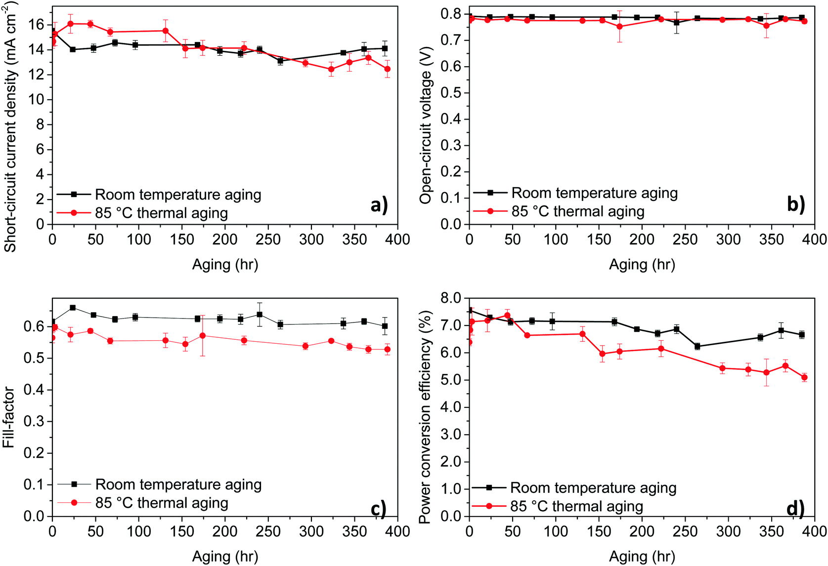 | ||
| Fig. 2 Device characteristic trends at room temperature aging and thermal aging at 85 °C under nitrogen of PPDT2FBT:PC61BM based OPVs. The results are from an average of 6 cells, with an active area of 0.1 cm2. | ||
For these temperatures, no significant burn-in loss was observed, rather, a constant and gradual decrease in the PCE due to the steady decrease in JSC and FF was present. Overall, though there is a gradual decrease in performance for PPDT2FBT:PC61BM devices heated up to the working temperature, there is a lack of a burn-in process that would otherwise significantly decrease the initial performance. It is worth noting that all the devices were taken out from the glove-box prior to J–V testing under ambient condition, the influence of air on the device performance cannot be eliminated.
The influence of the additional C70 on the device performances
Neat fullerene C70 was introduced previously as a third component to TQ1:C60 devices to enhance the performance by improving the thermal stability by suppressing crystal formation.58 Additionally, the use of C70 as an additive instead of C60 can improve light absorbance, which could potentially improve the current density of the device. Lastly, it was shown, with the support of Differential Scanning Calorimetry, for the addition of C70 to the TQ1:PC61BM blend, the neat fullerene acted as a nucleating agenting, thus, could improve the thermal stability, similar to C60.42 The study, did not, however, investigate the thermal degradation of device performance. To study the influence of additional C70 on the photovoltaic performances on PPDT2FBT:PC61BM based OPVs, different amounts of C70 was introduced to the active material blends and the donor–acceptor ratio was kept constant (1:2). The device performances with different additional amount of C70 are listed in Table 1. It is worth noting that TQ1-polymer is known to be amorphous in nature,59,60 whereas PPDT2FBT-polymer is known to have semi-crystalline properties.49,61
| PPDT2FBT:PC61BM:C70 (w:w:w) | J SC (mA cm−2) | V OC (V) | FF | PCE (%) |
|---|---|---|---|---|
| Average cell no. 6 cells/device area: 0.1 cm2/inverted devices coating conditions: flow-rate: 0.050 m min−1/drum-speed: 0.2 m min−1/ink concentration: 14.0 mg mL−1. | ||||
| 1:2:0 |
15.9 ± 0.3 | 0.80 ± 0.00 | 0.62 ± 0.01 | 7.27 ± 0.09 |
| 1:1.9:0.1 |
15.9 ± 0.5 | 0.74 ± 0.01 | 0.61 ± 0.01 | 7.16 ± 0.24 |
| 1:1.8:0.2 |
16.9 ± 0.5 | 0.72 ± 0.01 | 0.53 ± 0.02 | 6.47 ± 0.16 |
| 1:1.6:0.4 |
17.4 ± 1.5 | 0.70 ± 0.01 | 0.53 ± 0.03 | 6.47 ± 0.48 |
It was observed that the addition of more C70 into the active layer led to a significant increase in JSC due to the increased light absorption and a decrease in the VOC. However, the additional of C70 did not improve the PCE. For comparison 5% w/w of C60 with respect to PCBM was also added to the PPDT2FBT:PC61BM blend and was able to achieve an average JSC of 15.6 mA cm−2, VOC of 0.76 V, FF of 0.57, and PCE of 6.72%. Initially, it was suspected that the energy level alignment of materials was influencing the performance of the devices, especially the VOC. To confirm this, square-wave voltammetry (SWV) was measured for pristine materials (PPDT2FBT, PC61BM, PC71BM, C60 & C70). The energy level results from the SWV are illustrated in Fig. 3, (SWV curves can be found in the ESI,† Fig. S1).
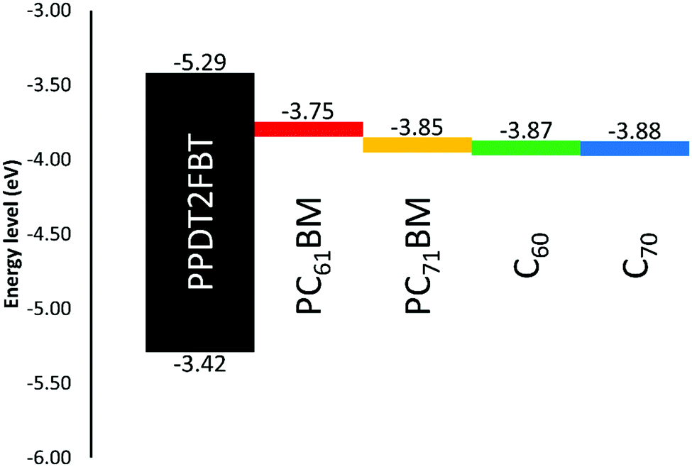 | ||
| Fig. 3 Illustration of energy levels of the active layer materials estimated from square-wave voltammetry measurements under identical conditions; PPDT2FBT (HOMO/LUMO), PC61BM, PC71BM, C60 & C70 (LUMO only). | ||
As seen in Fig. 3, there is a reduction between the energy difference between the HOMOpolymer/LUMOneat fullerene than that compared to the HOMOpolymer/LUMOPC61BM. It has been shown that the open-circuit voltage of OPVs is strongly influenced by the energy difference between the HOMOdonor and the LUMOacceptor levels.62,63 In the case of the fullerene acceptors, the C60 and C70 have relatively lower LUMO levels (−4.12 and −4.13 eV respectively) when compared with PC61BM and PC71BM (−3.99 and −4.10 eV). Hence, the addition of neat fullerenes to the active layer blend led to the decrease in VOC when compared with the binary system. Furthermore, the increased amount of C70 also resulted in a further decrease in the VOC.
Though C60 was observed to have a higher LUMO level than C70, the addition of C60 resulted in a reduced performance. This difference is accredited the significant decrease in the fill-factor, having dropped down to 0.57. It is known that nucleating agents, such as small molecules, can influence the morphology of active layer blends,64,65 therefore, the addition of C60 could have negatively influenced the PPDT2FBT:PC61BM blend, resulting in a decreased efficiency.
Overall, the difference in energy level alignment between active layer materials resulted in the reduced performance of the devices. To minimise the impact of the neat fullerene addition on VOC, 5% w/w of C70 was selected for further stability studies and 5% w/w of C60 was also investigated for comparison.
Thermal stability at 120 °C
As discussed above, it is observed that the PPDT2FBT:PC61BM was fairly stable at RT and 85 °C, only showing a slow gradual decrease in JSC, FF, and PCE over long term storage. To test the device stability under accelerated condition, 120 °C was used as the aging temperature, and the device performances were tested for the cells with and without additional neat fullerene. Furthermore, this temperature has been reported to induce a significant burn-in process to slot-die coated PPDT2FBT:PC71BM inverted devices.47Fullerene C60 has been previously reported to improve thermal stability by acting as a nucleating agent when introduced to TQ1:fullerene based devices.42 In that study C60 was found to be a better nucleating agent for PCBM than C70, however, C70 would also result in decreased crystal size and increased crystal population. As of this, C60 and C70 addition to the BHJ was performed to see if it can improve the thermal stability of the devices in this work. The idea is that the nucleating agents will induce the growth of many small crystals instead of a few large ones, resulting in suppressed performance reduction.
With this in mind, PPDT2FBT:PC61BM, PPDT2FBT:PC61BM:C60 and PPDT2FBT:PC61BM:C70 devices were fabricated and thermally aged at 120 °C under dark conditions in under nitrogen atmosphere, while device testing, itself, was performed in air at room temperature. The results of the thermal aging can be seen in Fig. 4 (table of results can be found in the ESI†).
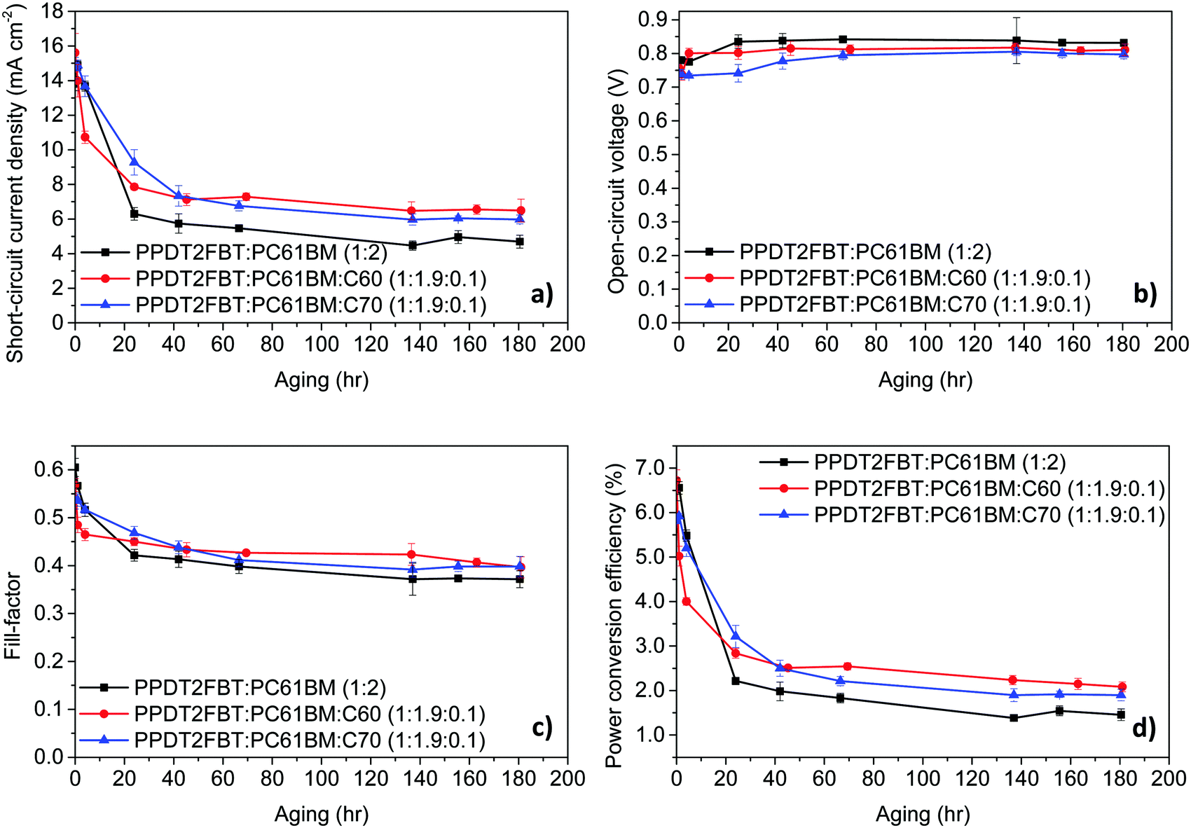 | ||
| Fig. 4 Device characteristics trends at 120 °C thermal aging under nitrogen. The results are from an average of 6 cells, with an active area of 0.1 cm2. | ||
It was found that when the devices were aged at 120 °C, there are several trends that are common to all systems. Firstly, there is a significant decrease in the JSC and FF with different degrees of thermal “burn-in” occurring in the first 24–48 hours. These changes in JSC and FF are suspected to be a result from the morphology change in the BHJ layer, with the PC61BM likely to crystallize under heated conditions.66,67 As for the VOC, all systems had seen an increase within the first 80 hours before remaining constant. The increase in the VOC is likely due to the elimination of the energy disorder at the BHJ/ZnO interface, which has also been observed for BTID-2F:PC71BM devices when stored under dark conditions.68
With the addition of C60 to the active layer, there is a fast “burn-in” within 4 hours of aging, however, the degree of a performance drop is less than the PPDT2FBT:PC61BM. It is also observed that after the initial burn-in, the devices remained stable with a slightly higher PCE. As for the addition of C70, the burn-in loss is slower, having lasted for around 40 hours instead of 48 hours for the binary blend and 20 hours after the addition of C60. It is also noted that the burn-in loss is less than for PPDT2FBT:PC61BM. Once the burn-in process has passed, the degradation of the ternary blends follows a similar rate to that of the binary PPDT2FBT:PC61BM devices.
Overall, the addition of C70 was able to improve the thermal stability of PPDT2FBT:PC61BM devices by reducing the impact from the thermal burn-in process at 120 °C, whereas the addition of C60, resulted in a faster burn-in process with slightly higher performing devices over longer times.
Imaging of microcrystals at BHJ surface
To investigate the morphological change during thermal aging, half-devices (PET/ITO/ZnO NP/BHJ) were heated at 120 °C for 8 hours under nitrogen. The BHJ layers before and after 120 °C heating was characterised under SEM and the images are shown in Fig. 5. Without heating, all BHJ layers were observed to be smooth and free of aggregates/crystals, but after thermal annealing, micro-sized crystals were formed on the BHJ/air surface.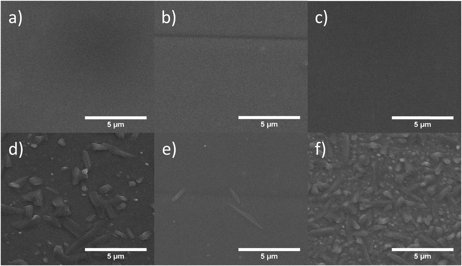 | ||
| Fig. 5 SEM images of PPDT2FBT:PC61BM (1:2) (a and d), PPDT2FBT:PC61BM:C70 (1:1.9:0.1) (b and e) & PPDT2FBT:PC61BM:C60 (1:1.9:0.1) (c and f) before (a–c) and after (d–f) heated for 8 h at 120 °C under dark nitrogen conditions. | ||
We also found that different annealed BHJ layers showed slightly different degrees and shapes of crystals on the surface. It was assumed that these crystals on the surface were most likely consisting of PC61BM, consistent with previous reports.
For PPDT2FBT:PC61BM, relatively large crystals had appeared on the surface after heating, which could be a result from the crystallisation of PC61BM. In the case of the PPDT2FBT:PC61BM:C60, the size of the crystals is smaller than those seen with PPDT2FBT:PC61BM, the number of them present at the surface has significantly increased. This behaviour is consistent with earlier studies that the addition of C60 can act as a nucleating agent. After the addition of C70, there is a significant reduction of the number of crystals compared to the other samples.
As C60 acts as a nucleating agent, crystal nuclei are formed to allow for crystal growth, thus, more crystals are created. As there is limited space within the film inside the devices, the growth of the crystals is restricted. This can explain why there is a steeper burn-in process as the crystals begin to grow, however, due to the restricted crystal size, the magnitude of the faster decrease is not as severe after the addition of C70 as the decrease seen in the PPDT2FBT:PC61BM. The addition of C70 is significantly reducing the crystallisation rate of PC61BM in the PPDT2FBT:PC61BM blend, visible in both a slower burn-in and crystallisation process. In literature, it was determined that the addition of C70 into the TQ1:PC61BM blends, would result in the neat fullerene acting as a nucleating agent,42 however, this does not appear to be the case in this study.
Next, we investigated how the performance degradation differed between devices that were annealed at 120 °C for 24 hours before and after deposition MoOX/Al on top of the BHJ. As seen in Fig. 5, the crystals had appeared at the top surface of the BHJ, which could result in a layer of fullerene at BHJ/MoOX interface. The JV-curves of devices at different annealing stages can be seen in Fig. S2 in the ESI.†
For devices that were annealed after completion of the fabrication, though there is a change in the shape of the J–V curve, it still showed photovoltaic effect (above 1% PCE). As for those devices heated prior to MoOX/Al deposition, the efficiency is very low (below 0.1% PCE).
Without the coating on top of the BHJ layers, there is space for the microcrystals to grow above the surface of the BHJ. As for the complete devices, the top and bottom sides of the BHJ are “blocked” by interface materials (MoOX & ZnO NP respectively), preventing the crystals from growing outside of the layer. This likely explains the performance difference between devices heated before and after MoOX/Al deposition.
Elemental characteristics of microcrystals
To further understand the origin of the microcrystals, auger electron spectroscopy (AES) was used to detect the presence of different elements on different features on the annealed (120 °C, 24 h) PPDT2FBT:PC61BM surface. The advantage of the technique is that it is allowed for specific scanning areas with an effective analysis depth of around 10 nm,69 meaning that the underlying BHJ/interface/electrode should not interfere with the measurements. Understanding that the layer consisted of a combination of PPDT2FBT and PC61BM, it was suspected that carbon, nitrogen, oxygen, fluorine, and sulphur peaks would be present in the spectra.From the AES spectra (Fig. 6), it was found that both carbon (272 eV70) and sulphur (152 eV70) were the easiest to resolve from the background signal. Whereas oxygen (508 eV70) was more difficult to resolve, yet, could still be resolvable in some spectra. Lastly, nitrogen (379 eV70) and Fluorine (647 eV70) were incredibly difficult to resolve from the background, with most times the peaks for these elements not being able to be observed entirely. To give a quantitative comparison between positions, the sulphur to carbon ratio was compared. As of this, the carbon/sulphur ratio was compared to estimate material composition.
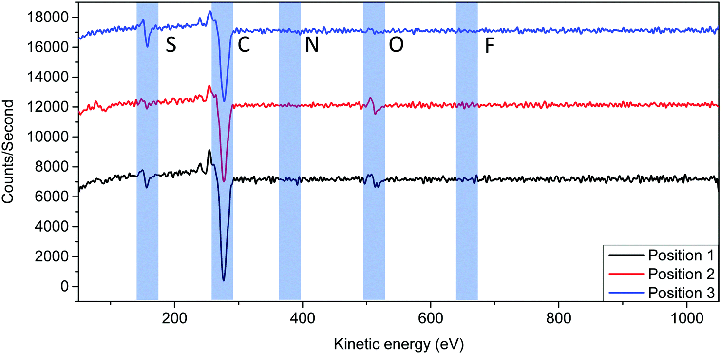 | ||
| Fig. 6 Flattened and smoothed Auger spectrums of three positions that were measured on the PPDT2FBT:PC61BM surface, including the predicted peak position of elements of interest. The spectrums are an average of 5 different scanning areas. | ||
This difference in peak intensity can be attributed to two factors, amount of the element present and the sensitivity factor. When operating an electron beam at 10 keV, the sensitivity factors for carbon, nitrogen, oxygen, fluorine and sulphur are 0.28, 0.60, 0.79, 1.91 and 2.43, respectively.71 As sulphur has a relatively high factor, a low amount of sulphur results in a resolvable peak, whereas carbon, even though having a low factor, there is a large amount of the element present in both materials. For oxygen, even though it has a lower peak, the element is present in both polymer and fullerene materials. Lastly, both nitrogen and fluorine have a low sensitivity factor, plus is only present in the polymer material, resulting in peak intensities that would be difficult to resolve from the background. As both carbon and sulphur were easy to resolve, the analysis of the spectra involved the comparison between these two elements.
For the investigation, 3 positions were measured using “point scan” of the specific locations. These include short crystals (position 1), long crystals (position 2) and the surface of the active layer (position 3). For the BHJ (position 3), it was suspected that these locations contained a mixture of PC61BM and PPDT2FBT. To determine what material the crystals consisted of, it was hypothesised that if a feature was PPDT2FBT, an increase in sulphur would accord compared to position 3 spectra, while, a decrease in sulphur would indicate the presence of PC61BM. The experimental spectra from the scans can be found in the ESI,† while the resulting atomic composition % can be found in Table 2.
| Position | Description | Carbon % | Sulphur % |
|---|---|---|---|
| 1 | “Short” crystal | 98.2 ± 0.2 | 1.8 ± 0.2 |
| 2 | “Long” crystal | 98.4 ± 0.3 | 1.6 ± 0.3 |
| 3 | BHJ surface | 96.5 ± 0.2 | 3.5 ± 0.2 |
From the Table 2, position 1 and 2, scanning on the crystals, show a decrease in the presence when compared with position 3. The two crystal positions are within significant figures of each other. Also, from the scans, the oxygen peaks associated with position 2 & 3 are resolvable. This supports the hypothesis that the micro-crystals that formed during thermal aging at 120 °C consists of PC61BM. In cases that sulphur is detected, it is likely as the fullerene grows and moves up from the surface, some of the polymer is taken up with it, remaining on the surface of the crystal. Another likely source of sulphur is the surroundings of the crystal being detected, with the diameter of the beam during the scan being approximately 650 nm. As some of the crystals had similar sizes as the beam, it is likely that the beam was also analysing the surface of the BHJ, especially for position 1 scans. Overall, with support from the Auger microscopy measurements, it is likely that the microcrystals at the surface of the BHJ consists of fullerene.
Thermal analysis
In OPV research, dynamic mechanical thermal analysis (DMTA) technique was previously used to understand the thermal transitions of pure materials and blends and is a useful tool to characterise the morphology of BHJ layer.54,72,73 In this work, it was used to understand the effect of annealing on the BHJ layers and to study the difference among binary blend and the ternary ones with the addition of C60 or C70.In the DMTA scans, E′ reflects the stiffness, E′′ peak feature suggests the thermal transitions, and tan delta = E′′/E′. Traditionally, the peak temperature of the tan delta peak is commonly used to define the thermal transition temperatures.
The DMTA scans of pure PPDT2FBT and BHJ blends are presented in Fig. 7. To reduce the amount of conjugated materials, woven glass fibre mesh was used as a support, thus the absolute value of E′ cannot be used to characterise the sample rigidity. Instead, the trend of E′ and E′′ change during heating is the main focus in the following discussion. Similar sample dimensions and amounts of materials are used so qualitative comparison of the data in Fig. 7 can be made.
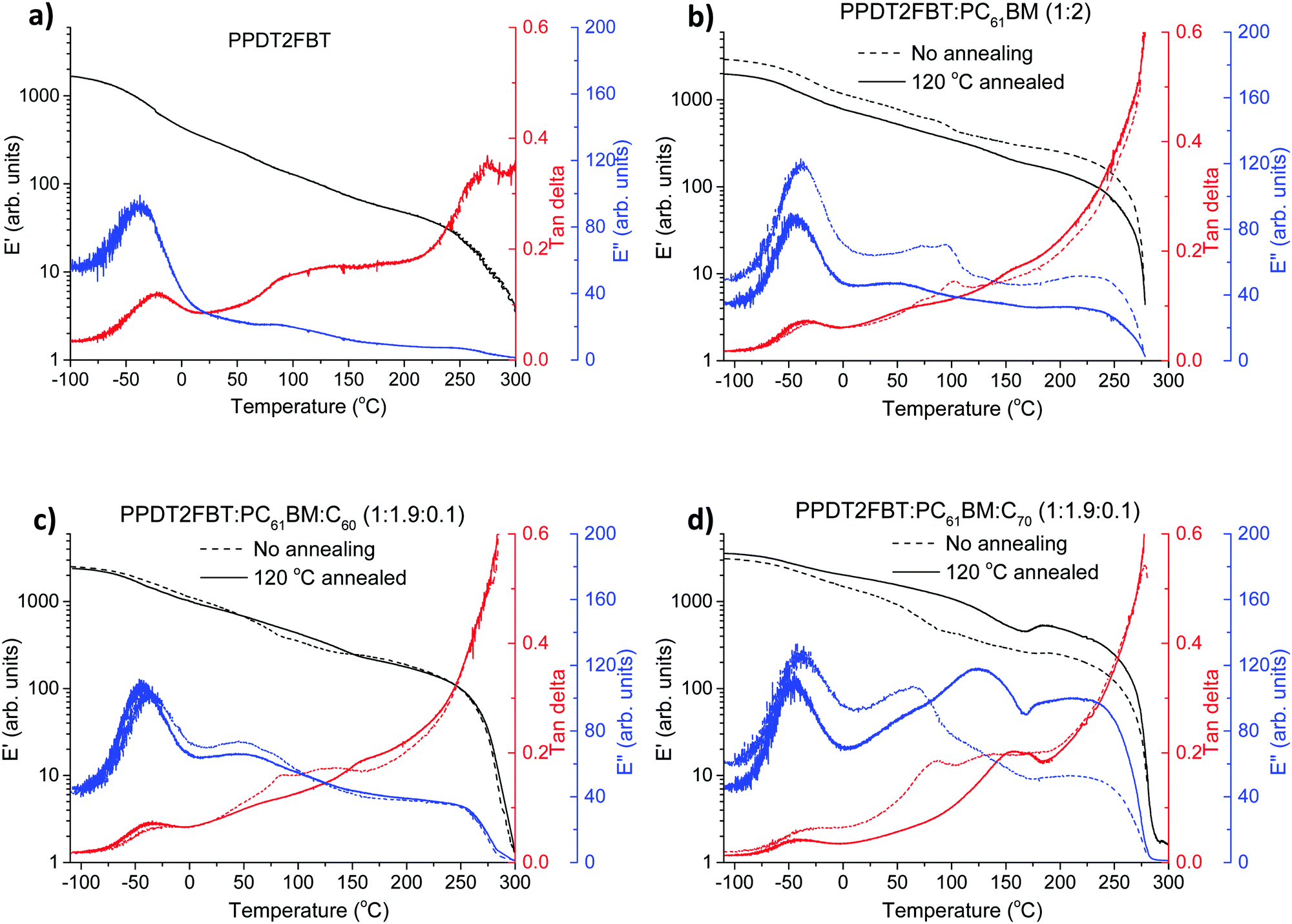 | ||
| Fig. 7 DMTA plots of pristine PPDT2FBT (a), PPDT2FBT:PC61BM (b), PPDT2FBT:PC61BM:C60 (c) and PPDT2FBT:PC61BM:C70 (d) before and after annealing (30 min). | ||
For pure PPDT2FBT, one sub-Tg is observed at around −25 °C (extracted from tan delta peak temperature), and no clear Tg was detected, indicating the lack of amorphous phase in the solid state54 of the pure polymer, in accordance with previously published works describing similar polymers.54,74 In the case of PPDT2FBT:PC61BM blend, the sub-Tg peaks can still be clearly detected and there is no shift of the peak temperature, which further confirmed that this feature is not originated from a glass transition. When no annealing was applied on the binary sample before the DMTA measurement, one extra thermal relaxation was found at ∼100 °C, seen by the E′′ peak, which is not observable from the sample annealed at 120 °C for 30 min. This result indicates that the binary blend exhibits some mobility during heating, thus changes in the morphology of BHJ is expected when annealed at 120 °C. However, no clear cold crystallisation was detected, which seems to conflict with the SEM results. The conflicting results might be caused by the relatively fast heating during DMTA measurement (3 °C min−1) compared to long time annealing (8 h) of the SEM sample, the growth of crystals in the DMA sample were not quick enough to be reflected in increased E′.
With the addition of C60 into the PPDT2FBT:PC61BM blend, the previously observed feature at ∼100 °C in the binary sample is absent (Fig. 7c). The samples before and after annealing show almost identical thermal mechanical properties, suggesting the addition of C60 results in restricted mobility of the BHJ layer, possibly originating from already formed small crystals in the materials.
Differently, introducing C70 to the blend yielded a second transition temperature (tan delta) that shifts from 85 (non-annealed one) to ∼155 °C after annealing, which is suspected to be due to the formation of more pure phases, induced by heating. The non-annealed sample showed a minor E′ increase at ∼180 °C, indicating the crystal formation at this high temperature. After annealing at 120 °C for 30 min, clearer crystallisation was observed at 170 °C indicated by the E′ increase after the thermal relaxation of the fullerene rich phase.53 The reason of clearer crystallisation observed in annealed PPDT2FBT:PC61BM:C70 sample is indicative of the small crystal formation during 120 °C annealing, which further grow to larger crystals upon applying high thermal energy. By having the main crystallization at such a higher temperature, this system is expected to be more stable at the described aging condition. From the DMTA measurements it is clear that the addition of C60 and C70 alters the thermal behaviour of the blends in different ways. This explains why, with the addition of C70, the burn-in process rate is slightly slower than that of PPDT2FBT:PC61BM and PPDT2BT:PC61BM:C60 at 120 °C.
We assume that the addition of C70 will increase the thermal stability further at 85 °C based on the results derived from the accelerated aging experiments at 120 °C. Our results indicate that PPDT2FBT:PC61BM:C70 is a promising system for large scale printed OPVs.
4. Conclusion
In conclusion, the addition of as low as 5% w/w C70 (in respect to PC61BM) to the slot-die coated bulk-heterojunction of PPDT2FBT:PC61BM was successfully demonstrated to improve the thermal stability. Initially, we have optimised the ink preparation and the coating conditions to reach an average power conversion efficiency of 8.49% and 7.63% for PPDT2FBT:PC71BM and PPDT2FBT:PC61BM devices, respectively. A subsequent investigation of the thermal stability of PPDT2FBT:PC61BM at 85 °C revealed that there was no burn-in loss as was observed in 120 °C aged devices. With support of scanning electron microscopy and auger electron spectroscopy, it was found that the growth of fullerene-rich crystals in the bulk-heterojunction is the likely source of thermal degradation at 120 °C.Addition of C60 to the PPDT2FBT:PC61BM appeared to act as a nucleating agent, with increased number and reduced size of the crystals. In comparison with the addition of C70 to the PPDT2FBT:PC61BM, the magnitude and rate of the burn-in loss was significantly reduced. Subsequently, the C70 did not appear to behave as a nucleating agent, instead, it was found that the rate of crystal growth reduced with the addition of the neat fullerene. Our results demonstrate that the small addition of C70 could improve the thermal stability of slot-die coated OPVs.
Author contributions
Bradley Kirk worked on device fabrication and material characteristic measurements, as well as writing of the draft paper. Xun Pan prepared samples and performed DMTA measurements on active material blends, as well as results discussion and interpretation. Martyn Jevric synthesised and characterised the PPDT2FBT polymer used in OPV fabrication. Gunther Andersson provided helped with guidance and expert advice throughout the work. Mats Andersson provide funding and resources towards the work, as well as guidance through the work. All the authors contributed to the correction and revision of the manuscript.Conflicts of interest
There are no conflicts to declare.Acknowledgements
The authors acknowledge the Commonwealth of Australia through the access from the Australian Government Research Training Program (AGRTP) for providing funding to undertake a PhD Higher Degree Research program, with addition to Playford Trust for providing additional funding towards the research program. Work was partly funded by the Australia Renewable Energy Agency (ARENA). We acknowledge Flinders Microscopy and Microanalysis (FMMA) at Flinders University for providing access to the microscopy instrument and facilities. This work was performed in part at the South Australian node of the Australian National Fabrication Facility (ANFF) under the National Collaborative Research Infrastructure Strategy.References
- B. C. Thompson and J. M. J. Fréchet, Angew. Chem., Int. Ed., 2008, 47, 58–77 CrossRef CAS PubMed.
- P. M. Beaujuge and J. M. J. Fréchet, J. Am. Chem. Soc., 2011, 133, 20009–20029 CrossRef CAS PubMed.
- T. R. Andersen, F. Almyahi, N. A. Cooling, D. Elkington, L. Wiggins, A. Fahy, K. Feron, B. Vaughan, M. J. Griffith and A. J. Mozer, J. Mater. Chem. A, 2016, 4, 15986–15996 RSC.
- J. C. Hummelen, B. W. Knight, F. LePeq, F. Wudl, J. Yao and C. L. Wilkins, J. Org. Chem., 1995, 60, 532–538 CrossRef CAS.
- M. M. Wienk, J. M. Kroon, W. J. H. Verhees, J. Knol, J. C. Hummelen, P. A. van Hal and R. A. J. Janssen, Angew. Chem., Int. Ed., 2003, 42, 3371–3375 CrossRef CAS PubMed.
- S. Bao, H. Yang, H. Fan, J. Zhang, Z. Wei, C. Cui and Y. Li, Adv. Mater., 2021, 33, 2105301 CrossRef CAS PubMed.
- Y. Cai, Y. Li, R. Wang, H. Wu, Z. Chen, J. Zhang, Z. Ma, X. Hao, Y. Zhao, C. Zhang, F. Huang and Y. Sun, Adv. Mater., 2021, 33, 2101733 CrossRef CAS PubMed.
- J. Song, L. Zhu, C. Li, J. Xu, H. Wu, X. Zhang, Y. Zhang, Z. Tang, F. Liu and Y. Sun, Matter, 2021, 4, 2542–2552 CrossRef CAS.
- B. Zimmermann, H.-F. Schleiermacher, M. Niggemann, U. Würfel and S. Cells, Solar Energy Mater. Solar Cells, 2011, 95, 1587–1589 CrossRef CAS.
- Q. Wu, J. Guo, R. Sun, J. Guo, S. Jia, Y. Li, J. Wang and J. Min, Nano Energy, 2019, 61, 559–566 CrossRef CAS.
- H. Zhao, L. Zhang, H. B. Naveed, B. Lin, B. Zhao, K. Zhou, C. Gao, C. Zhang, C. Wang and W. Ma, ACS Appl. Mater. Interfaces, 2019, 11, 42392–42402 CrossRef CAS PubMed.
- L. Zhang, X. Xu, B. Lin, H. Zhao, T. Li, J. Xin, Z. Bi, G. Qiu, S. Guo, K. Zhou, X. Zhan and W. Ma, Adv. Mater., 2018, 30, 1805041 CrossRef PubMed.
- E. Pérez-Gutiérrez, J. Lozano, J. Gaspar-Tánori, J.-L. Maldonado, B. Gómez, L. López, L.-F. Amores-Tapia, O. Barbosa-García and M.-J. Percino, Sol. Energy, 2017, 146, 79–84 CrossRef.
- F. C. Krebs, M. Jørgensen, K. Norrman, O. Hagemann, J. Alstrup, T. D. Nielsen, J. Fyenbo, K. Larsen and J. Kristensen, Solar Energy Mater. Solar Cells, 2009, 93, 422–441 CrossRef CAS.
- M. Ylikunnari, M. Välimäki, K.-L. Väisänen, T. M. Kraft, R. Sliz, G. Corso, R. Po, R. Barbieri, C. Carbonera and G. Gorni, Flexible Printed Electron., 2020, 5, 014008 CrossRef CAS.
- P. He, J. Cao, H. Ding, C. Liu, J. Neilson, Z. Li, I. A. Kinloch and B. Derby, ACS Appl. Mater. Interfaces, 2019, 11, 32225–32234 CrossRef CAS PubMed.
- G. Susanna, L. Salamandra, T. M. Brown, A. Di Carlo, F. Brunetti and A. Reale, Solar Energy Mater. Solar Cells, 2011, 95, 1775–1778 CrossRef CAS.
- Z. Jiang, R. Rahmanian, S. Soltanian, R. Nouri, P. Servati, IEEE International Flexible Electronics Technology Conference (IFETC), 2019, pp. 1–2 Search PubMed.
- S. Waheed, S. Pareek, P. Sharma and S. Karak, Semicond. Sci. Technol., 2020, 36, 015002 CrossRef.
- H. S. Ryu, S. Y. Park, T. H. Lee, J. Y. Kim and H. Y. Woo, Nanoscale, 2020, 12, 5792–5804 RSC.
- R. Søndergaard, M. Hösel, D. Angmo, T. T. Larsen-Olsen and F. C. Krebs, Mater. Today, 2012, 15, 36–49 CrossRef.
- Z. Zhang, J. Miao, Z. Ding, B. Kan, B. Lin, X. Wan, W. Ma, Y. Chen, X. Long, C. Dou, J. Zhang, J. Liu and L. Wang, Nat. Commun., 2019, 10, 3271 CrossRef PubMed.
- N. Zheng, K. Mahmood, W. Zhong, F. Liu, P. Zhu, Z. Wang, B. Xie, Z. Chen, K. Zhang, L. Ying, F. Huang and Y. Cao, Nano Energy, 2019, 58, 724–731 CrossRef CAS.
- R. Meitzner, T. Faber, S. Alam, A. Amand, R. Roesch, M. Büttner, F. Herrmann-Westendorf, M. Presselt, L. Ciammaruchi and I. Visoly-Fisher, Solar Energy Mater. Solar Cells, 2019, 202, 110151 CrossRef CAS.
- M. Li, W. Zhang, H. Wang, L. Chen, C. Zheng and R. Chen, RSC Adv., 2017, 7, 31158–31163 RSC.
- C.-N. Weng, H.-C. Yang, C.-Y. Tsai, S.-H. Chen, Y.-S. Chen, C.-H. Chen, K.-M. Huang, H.-F. Meng, Y.-C. Chao and C.-Y. Chang, Sol. Energy, 2020, 199, 308–316 CrossRef CAS.
- N. Y. Doumon, G. Wang, R. C. Chiechi and L. J. A. Koster, J. Mater. Chem. C, 2017, 5, 6611–6619 RSC.
- B. Muhsin, R. Roesch, G. Gobsch and H. Hoppe, Solar Energy Mater. Solar Cells, 2014, 130, 551–554 CrossRef CAS.
- Y. Sun, L. Meng, X. Wan, Z. Guo, X. Ke, Z. Sun, K. Zhao, H. Zhang, C. Li and Y. Chen, Adv. Funct. Mater., 2021, 31, 2010000 CrossRef CAS.
- H. Kang, G. Kim, J. Kim, S. Kwon, H. Kim and K. Lee, Adv. Mater., 2016, 28, 7821–7861 CrossRef CAS PubMed.
- W. Greenbank, N. Djeddaoui, E. Destouesse, J. Lamminaho, M. Prete, L. Boukezzi, T. Ebel, L. Bessissa, H.-G. Rubahn, V. Turkovic and M. Madsen, Energy Technol., 2020, 8, 2000295 CrossRef CAS.
- L. Duan and A. Uddin, Adv. Sci., 2020, 7, 1903259 CrossRef CAS PubMed.
- N. Li, J. D. Perea, T. Kassar, M. Richter, T. Heumueller, G. J. Matt, Y. Hou, N. S. Güldal, H. Chen and S. Chen, Nat. Commun., 2017, 8, 1–9 CrossRef PubMed.
- C. L. Chochos, N. Leclerc, N. Gasparini, N. Zimmerman, E. Tatsi, A. Katsouras, D. Moschovas, E. Serpetzoglou, I. Konidakis and S. Fall, J. Mater. Chem. A, 2017, 5, 25064–25076 RSC.
- X. Tong, N. Wang, M. Slootsky, J. Yu and S. R. Forrest, Solar Energy Mater. Solar Cells, 2013, 118, 116–123 CrossRef CAS.
- B. Paci, A. Generosi, V. Rossi Albertini, P. Perfetti, R. de Bettignies, J. Leroy, M. Firon and C. Sentein, Appl. Phys. Lett., 2006, 89, 043507 CrossRef.
- J. W. Andreasen, S. A. Gevorgyan, C. M. Schlepütz and F. C. Krebs, Solar Energy Mater. Solar Cells, 2008, 92, 793–798 CrossRef CAS.
- X. Yang, J. Loos, S. C. Veenstra, W. J. Verhees, M. M. Wienk, J. M. Kroon, M. A. Michels and R. A. Janssen, Nano Lett., 2005, 5, 579–583 CrossRef CAS PubMed.
- F. C. Krebs, J. Alstrup, H. Spanggaard, K. Larsen and E. Kold, Solar Energy Mater. Solar Cells, 2004, 83, 293–300 CrossRef CAS.
- C. Lindqvist, A. Sanz-Velasco, E. Wang, O. Bäcke, S. Gustafsson, E. Olsson, M. R. Andersson and C. Müller, J. Mater. Chem. A, 2013, 1, 7174–7180 RSC.
- C. Lindqvist, Stability of Bulk-heterojunction Blends for Solar Cell Applications, Chalmers University of Technology, 2014 Search PubMed.
- C. Lindqvist, J. Bergqvist, C. C. Feng, S. Gustafsson, O. Bäcke, N. D. Treat, C. Bounioux, P. Henriksson, R. Kroon, E. Wang, A. Sanz-Velasco, P. M. Kristiansen, N. Stingelin, E. Olsson, O. Inganäs, M. R. Andersson and C. Müller, Adv. Energy Mater., 2014, 4, 1301437 CrossRef.
- A. Distler, C. J. Brabec and H.-J. Egelhaaf, Prog. Photovoltaics Res. Appl., 2021, 29, 24–31 CrossRef.
- M. Moser, A. Wadsworth, N. Gasparini and I. McCulloch, Adv. Energy Mater., 2021, 11, 2100056 CrossRef CAS.
- T. P. Osedach, T. L. Andrew and V. Bulović, Energy Environ. Sci., 2013, 6, 711–718 RSC.
- S. V. Dayneko, M. Pahlevani and G. C. Welch, ACS Appl. Mater. Interfaces, 2019, 11, 46017–46025 CrossRef CAS PubMed.
- S. Song, K. T. Lee, C. W. Koh, H. Shin, M. Gao, H. Y. Woo, D. Vak and J. Y. Kim, Energy Environ. Sci., 2018, 11, 3248–3255 RSC.
- M. Mainville, V. Tremblay, M. Z. Fenniri, A. Laventure, M. E. Farahat, R. Ambrose, G. C. Welch, I. G. Hill and M. Leclerc, Asian J. Org. Chem., 2020, 9, 1318–1325 CrossRef CAS.
- T. L. Nguyen, H. Choi, S. J. Ko, M. A. Uddin, B. Walker, S. Yum, J. E. Jeong, M. H. Yun, T. J. Shin and S. Hwang, Energy Environ. Sci., 2014, 7, 3040–3051 RSC.
- S.-C. Wu, L. T. Strover, X. Yao, X.-Q. Chen, W.-J. Xiao, L.-N. Liu, J. Wang, I. Visoly-Fisher, E. A. Katz and W.-S. Li, ACS Appl. Mater. Interfaces, 2018, 10, 35430–35440 CrossRef CAS PubMed.
- P.-O. Morin, T. Bura, B. Sun, S. I. Gorelsky, Y. Li and M. Leclerc, ACS Macro Lett., 2015, 4, 21–24 CrossRef CAS.
- F. C. Krebs, Solar Energy Mater. Solar Cells, 2008, 92, 715–726 CrossRef CAS.
- A. Sharma, X. Pan, J. A. Campbell, M. R. Andersson and D. A. Lewis, Macromolecules, 2017, 50, 3347–3354 CrossRef CAS.
- A. Sharma, X. Pan, J. M. Bjuggren, D. Gedefaw, X. Xu, R. Kroon, E. Wang, J. A. Campbell, D. A. Lewis and M. R. Andersson, Chem. Mater., 2019, 31, 6740–6749 CrossRef CAS.
- S.-C. Shin, C. W. Koh, P. Vincent, J. S. Goo, J.-H. Bae, J.-J. Lee, C. Shin, H. Kim, H. Y. Woo and J. W. Shim, Nano Energy, 2019, 58, 466–475 CrossRef CAS.
- M. O. Reese, S. A. Gevorgyan, M. Jørgensen, E. Bundgaard, S. R. Kurtz, D. S. Ginley, D. C. Olson, M. T. Lloyd, P. Morvillo, E. A. Katz, A. Elschner, O. Haillant, T. R. Currier, V. Shrotriya, M. Hermenau, M. Riede, K. R. Kirov, G. Trimmel, T. Rath, O. Inganäs, F. Zhang, M. Andersson, K. Tvingstedt, M. Lira-Cantu, D. Laird, C. McGuiness, S. Gowrisanker, M. Pannone, M. Xiao, J. Hauch, R. Steim, D. M. DeLongchamp, R. Rösch, H. Hoppe, N. Espinosa, A. Urbina, G. Yaman-Uzunoglu, J.-B. Bonekamp, A. J. J. M. van Breemen, C. Girotto, E. Voroshazi and F. C. Krebs, Solar Energy Mater. Solar Cells, 2011, 95, 1253–1267 CrossRef CAS.
- M. V. Khenkin, E. A. Katz, A. Abate, G. Bardizza, J. J. Berry, C. Brabec, F. Brunetti, V. Bulović, Q. Burlingame and A. Di Carlo, Nat. Energy, 2020, 5, 35–49 CrossRef.
- A. D. de Zerio Mendaza, J. Bergqvist, O. Bäcke, C. Lindqvist, R. Kroon, F. Gao, M. R. Andersson, E. Olsson, O. Inganäs and C. Müller, J. Mater. Chem. A, 2014, 2, 14354–14359 RSC.
- E. Wang, J. Bergqvist, K. Vandewal, Z. Ma, L. Hou, A. Lundin, S. Himmelberger, A. Salleo, C. Müller and O. Inganäs, Adv. Energy Mater., 2013, 3, 806–814 CrossRef CAS.
- J. Bergqvist, C. Lindqvist, O. Bäcke, Z. Ma, Z. Tang, W. Tress, S. Gustafsson, E. Wang, E. Olsson and M. R. Andersson, J. Mater. Chem. A, 2014, 2, 6146–6152 RSC.
- H. Kang, M. A. Uddin, C. Lee, K.-H. Kim, T. L. Nguyen, W. Lee, Y. Li, C. Wang, H. Y. Woo and B. J. Kim, J. Am. Chem. Soc., 2015, 137, 2359–2365 CrossRef CAS PubMed.
- D. Mühlbacher, M. Scharber, M. Morana, Z. Zhu, D. Waller, R. Gaudiana and C. Brabec, Adv. Mater., 2006, 18, 2884–2889 CrossRef.
- C. J. Brabec, N. S. Sariciftci and J. C. Hummelen, Adv. Funct. Mater., 2001, 11, 15–26 CrossRef CAS.
- A. Sharenko, N. D. Treat, J. A. Love, M. F. Toney, N. Stingelin and T.-Q. Nguyen, J. Mater. Chem. A, 2014, 2, 15717–15721 RSC.
- H.-C. Liao, P.-H. Chen, R. P. H. Chang and W.-F. Su, Polymers, 2014, 6, 2784–2802 CrossRef.
- J. Zhao, A. Swinnen, G. Van Assche, J. Manca, D. Vanderzande and B. V. Mele, J. Phys. Chem. B, 2009, 113, 1587–1591 CrossRef CAS PubMed.
- S. Bertho, G. Janssen, T. J. Cleij, B. Conings, W. Moons, A. Gadisa, J. D’Haen, E. Goovaerts, L. Lutsen and J. Manca, Solar Energy Mater. Solar Cells, 2008, 92, 753–760 CrossRef CAS.
- R. Sun, D. Deng, J. Guo, Q. Wu, J. Guo, M. Shi, K. Shi, T. Wang, L. Xue and Z. Wei, Energy Environ. Sci., 2019, 12, 2518–2528 RSC.
- R. P. Gunawardane and C. R. Arumainayagam, Handbook of applied solid state spectroscopy, Springer, 2006, pp. 451–483 Search PubMed.
- J. C. Vickerman and I. S. Gilmore, Surface analysis: the principal techniques, John Wiley & Sons, 2011 Search PubMed.
- K. D. Childs, B. A. Carlson, L. A. LaVanier, J. F. Moulder, D. F. Paul, W. F. Stickle and D. G. Watson, Handbook of Auger Electron Microscopy, Physical Electronics, Inc., Eden Prairie, Minnesota, 3rd edn, 1997 Search PubMed.
- L. Yu, D. Qian, S. Marina, F. A. A. Nugroho, A. Sharma, S. Hultmark, A. I. Hofmann, R. Kroon, J. Benduhn and D.-M. Smilgies, ACS Appl. Mater. Interfaces, 2019, 11, 21766–21774 CrossRef CAS PubMed.
- X. Pan, A. Sharma, D. Gedefaw, R. Kroon, A. D. de Zerio, N. P. Holmes, A. L. D. Kilcoyne, M. G. Barr, A. Fahy and M. Marks, Org. Electron., 2018, 59, 432–440 CrossRef CAS.
- N. Balar, S. Siddika, S. Kashani, Z. Peng, J. J. Rech, L. Ye, W. You, H. Ade and B. T. O’Connor, Chem. Mater., 2020, 32, 6540–6549 CrossRef CAS.
Footnote |
| † Electronic supplementary information (ESI) available. See DOI: 10.1039/d2ma00120a |
| This journal is © The Royal Society of Chemistry 2022 |