
 Open Access Article
 This Open Access Article is licensed under a
 Creative Commons Attribution 3.0 Unported Licence
Prediction of new phase 2D C2h group III monochalcogenides with direct bandgaps and highly anisotropic carrier mobilities†
Tuo
Hu‡
ab,
Congsheng
Xu‡
a,
Ao
Zhang
c and
Peiyuan
Yu
 *a
*a
aDepartment of Chemistry and Shenzhen Grubbs Institute, Southern University of Science and Technology, Shenzhen, 518055, China. E-mail: yupy@sustech.edu.cn
bDepartment of Chemistry and Biochemistry, University of California, Los Angeles, CA 90095, USA
cDepartment of Physics, Southern University of Science and Technology, Shenzhen, 518055, China
First published on 25th January 2022
Abstract
Two-dimensional (2D) group III monochalcogenides (MX, M = Ga, In and X = S, Se, Te) are promising candidates for next-generation ultrathin optoelectronic devices due to their exotic properties. However, the lack of direct band gaps and the low hole mobilities in their conventional single-layer D3h phase hinder their potential utility for various applications. In this work, new polymorphs of 2D MXs belonging to the space group C2h are predicted through a global structural search based on artificial swarm intelligence and density functional theory calculations. We demonstrate that such monolayer polymorphs are thermodynamically and kinetically stable through phonon spectrum analysis and ab initio molecular dynamics simulations. Direct band gaps of 2.38 to 2.84 eV are revealed in all C2h MX monolayers, a property that traditional 2D D3h MXs do not possess. Calculations based on the Boltzmann Transport Equation method show that electron mobilities in C2h monolayers are significantly higher in magnitude than those of the conventional D3h phase. Anisotropic optical properties are predicted and high absorption coefficients covering the UV-visible spectra are also reported. All these features render the new C2h MX monolayers promising candidates for potential applications in high-efficiency solar cells and anisotropic optoelectronic devices.
1. Introduction
Since the discovery of graphene by Novoselov and Geim in 2004, atomically thin 2D materials have been a focal point in the quest for next-generation flexible nanoelectronics and optoelectronics in the post-Si era.1–7 In addition to the well-known graphene-like group IV semiconductors and group III–V binary compounds,8–10 both experimental and theoretical investigations have expanded the 2D-semiconductor family by the discovery of monolayer group IV monochalcogenides,11,12 transition metal dichalcogenides,13,14 black phosphorus,15,16 and group III monochalcogenides.17–22 Nevertheless, the zero band gap in graphene,11 low electron mobility in transition metal dichalcogenides,13 and the structural instability of black phosphorus under moisture conditions greatly restrict their applications.16 Therefore, novel 2D semiconductors with sizable band gaps, high carrier mobilities, and strong stability are in great request. Fortunately, polymorphic properties in these single-layer materials provide new probability to realize this goal. Examples include the coexistence of metallic octahedral (1T′) and semiconducting trigonal prismatic (2H) monolayer MoS223,24 as well as the presence of blue phosphorus with wider band gaps compared to the black phosphorus polymorphs.25 Therefore, the exploration of monolayer polymorphs of known semiconductors leave room for the discovery of unexpected properties and emergent applications.Among these 2D materials, group III monochalcogenides (MX), represented by InSe, have attracted growing research attention because of their idiosyncratic optoelectronic properties and their promising potential applications as field-effect transistors,17,21 photodetectors,26–28 and photocatalysts.30 Significant efforts have also been spent on investigating the polymorphic nature of MXs. Take InSe as an example. Its most stable 2D structure takes a graphene-like honeycomb lattice, featured by a non-centrosymmetric D3h point group.17 Bulk InSe consisting of D3h layers are found to have a direct band gap of about 1.3 eV, but it increases to an indirect band gap of 2 eV as the sample thickness decreases to the atomic scale.22 Moreover, room-temperature hole mobility in D3h monolayer InSe is only 4.8 cm2 V−1 s−1.29 The lack of a direct band gap and the low hole mobility would severely restrict the optoelectronic applications of D3h monolayer InSe. Recently, a new monolayer polymorph of InSe belonging to the D3d point group has been theoretically predicted via the Particle Swarm Optimization (PSO) method, followed by the experimental synthesis of single-layer D3d GaSe sheets.31 Although this new phase is reported to possess a wider band gap and a higher electron mobility,31,33 there are still some shortcomings that are not fully addressed, such as the absence of a direct band gap and the low hole mobility.
Here, we further explore the polymorphic nature of 2D MX semiconductors through artificial swarm intelligence computational structural searches on CALYPSO (Crystal structure AnaLYsis by Particle Swarm Optimization)36 and ab initio calculations using the Vienna ab initio simulation package (VASP) software,37–40 and identified a monolayer phase belonging to the C2h point group. It is reported that bulk C2h InSe with a direct band gap has in fact been experimentally synthesized,34,35 which hints the possibility of fabricating C2h monolayers whose properties were largely unknown. We demonstrate the thermodynamic and kinetic stability of the identified C2h monolayers through phonon spectrum analyses and ab initio molecular dynamics (AIMD). We carried out first-principles computations on the electrical and optical properties of single-layer C2h MXs and discovered that they all have intrinsic wide direct bandgaps located in the visible spectrum. Furthermore, anisotropic carrier mobilities are reported. It is noteworthy to point out that while C2h MXs have electron mobilities that are comparable to those of conventional C2h monolayers, their hole mobilities are significantly higher than those in D3h sheets. Anisotropic optical properties of 2D C2h MXs with higher linear absorption coefficients in the UV-visible spectra are also observed. Such superior properties render the C2h III–VI binary 2D semiconductors worthwhile for further studies to shape them into promising candidates for high-performance electronics and optoelectronics.
2. Computational methods
Structural prediction through artificial swarm intelligence computational structure searches on CALYPSO (Crystal structure AnaLYsis by Particle Swarm Optimization)36 is applied systematically to the most discussed binary MXs in the III–VI family, namely InSe, InS, GaSe, and GaS.17–32 Detailed information regarding this method can be found in the ESI.†Ab initio molecular dynamics (AIMD) calculations were performed through the Vienna ab initio simulation package (VASP) software37–40 using the NVT ensemble in which the temperature was held constant at 300 K in the Nose–Hoover thermostats.41 All molecular dynamics (MD) calculations were performed on the 4 × 4 × 1 supercells of single-layer MX compounds whose k-spaces were sampled by a 2 × 2 × 1 grid, and all simulations applied a time step of 2 fs, lasting for 10 ps (5000 steps). The phonon dispersion spectra were obtained using density functional perturbation theory (DFPT) as implemented in PWscf (Quantum ESPRESSO package)42–44 with a planewaves cutoff of 60 Ry. A 20 × 20 × 1 k-sampling and a 5 × 5 × 1 phonon grid were utilized in the phonon dispersion calculations.
Density functional theory (DFT) calculations on the properties of 2D C2h MXs were carried out based on the generalized gradient approximation (GGA) along with the exchange–correlation functional proposed by Perdew, Burke, and Ernzerhof (PBE)45,46 as implemented in VASP. The projected augmented-wave (PAW) pseudopotentials were utilized for the description of the electron–ion interactions in the systems,47,48 and an energy cutoff of 400 eV was adopted for the plane-wave basis set. For all calculations associated with the 2D structures and properties, a vacuum slab of 20 Å was inserted along the c-axis to avoid interactions between the periodic images on the perpendicular directions. For geometry optimizations and electronic structure calculations, 20 × 20 × 1 Monkhorst–Pack meshes were applied to sample the Brillouin zone. The lattice structures and atomic positions were relaxed using the conjugated gradient method, and the equilibrium configurations of the systems are determined once the residual energy and force meet their convergence criteria, which are set to be 1 × 10⁻⁸ eV and 0.001 eV Å−1 respectively. The Heyd–Scuseria–Ernzerhof (HSE06) hybrid functional was adopted to obtain more accurate band structures.49
The carrier mobilities were obtained using the EPW code based on the ab initio Boltzmann transport equation (BTE)50 which expresses the mobility μe as

 ; its occupation distribution at equilibrium (f(n, k)) is derived according to the Boltzmann distribution function:
  , where kB and T are the Boltzmann constant and the system temperature respectively.
Carrier mobility computation using the EPW code also involves the calculation of the electron–phonon coupling (EPC) matrix.51 In our study, the EPC matrix elements were computed through DFPT calculations on a 100 × 100 × 2 k-grid and a 100 × 100 × 2 q-grid. Moreover, the carrier concentration was set to be 1013 cm−3 for all systems when calculating the mobilities.
Carrier effective mass is calculated using the following equation:
 is the curvature of the electronic band.
The optical absorption coefficients of the MXs are derived from the frequency-dependent complex dielectric function calculated with the HSE06 method:
 and
and  stand for the real and imaginary part of the dielectric function, respectively. With the complex dielectric function at hand, the absorption coefficient (α) can be derived from the following equation:
3. Results and discussion
3.1. Structural search
After unbiased global structural searches based on the PSO algorithm, 3600 possible structures per MX compound are sampled from the free energy landscape, and the ones among them with relatively low energies are mainly composed of three monolayer polymorphs. Structural predictions of InSe in our study are consistent with the results reported in Zhang's study.31 The lowest-energy structure (Fig. 1a) corresponds to the experimentally known D3h monolayer. Another polymorph belonging to the D3d space group is found to have an energy comparable to that of the D3h structure, which has been thoroughly explored in Zhang's study.31 The D3d phase is beyond the scope of our study, thus not discussed here. The polymorph shown in Fig. 1b is a monoclinic lamellae phase belonging to the C2h point group. Distinct from the conventional D3h phase with four atoms per unit cell, the C2h phase features a larger unit cell in which eight atoms are included.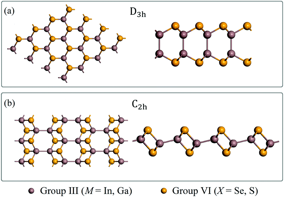 | ||
| Fig. 1 The monolayer structures of (a) D3h and (b) C2h MXs. The top and side views are presented on the left and the right side of each panel respectively. The structural coordinates of C2h monolayers can be found in the ESI.† | ||
The lattice constants of the fully relaxed MX monolayers predicted by CALYPSO are tabulated in Table 1. For 2D C2h InSe, its optimized lattice parameters are a = 11.23 Å, b = 4.10 Å, which show significant similarity to the experimental data of the bulk sample (a = 11.74 Å, b = 4.11 Å).33 Since the C2h phase of these compounds except for InSe has not been studied before, there are no theoretical or experimental data in previous literature to compare with. Data in Table 1 indicate that the lattice constants b are approximately the same for both of the D3h and C2h phases while the lattice parameters a in C2h MXs are about three times larger than those in D3h monolayers. As shown in Fig. 1b, the vertically aligned M–M bonds in the D3h phase adopt a nearly horizontal orientation in the C2h unit cell, making the latter phase distinct from the graphene-like honeycomb lattice of the former one (Fig. 1a). This structural feature also endows the C2h structure with potential anisotropic properties along the horizontal axes. Moreover, the presence of inversion symmetry in the C2h phase differentiates itself from the non-centrosymmetric D3h phase.
| a (Å) | b (Å) | E c (eV per atom) | ||
|---|---|---|---|---|
| InSe | D 3h | 4.08 | 4.08 | 3.543 |
| C 2h | 11.23 | 4.10 | 3.504 | |
| InS | D 3h | 3.93 | 3.93 | 3.847 |
| C 2h | 11.08 | 3.97 | 3.810 | |
| GaSe | D 3h | 3.81 | 3.82 | 3.795 |
| C 2h | 9.97 | 3.82 | 3.746 | |
| GaS | D 3h | 3.63 | 3.63 | 4.158 |
| C 2h | 9.81 | 3.65 | 4.109 |
3.2. Thermodynamic and kinetic stability
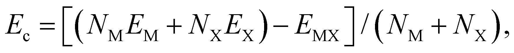
Cohesive energy (Ec) calculations are carried out based on the following expression, and the corresponding data are recorded in Table 1.where NM and NX are the number of group III (M) and VI (X) atoms per unit cell respectively, while EM and EX stand for the single atom energies of their corresponding elements, and EMX is the system's total energy. It is indicated in Table 1 that there is an energy difference of about 40 to 50 meV per atom between the energetically less favored C2h polymorph and the common D3h phase for all III–VI compounds. This difference in cohesive energy for GaX compounds (49 meV per atom for both GaSe and GaS) is larger than that in InX compounds (39 meV per atom for InSe and 37 meV per atom for InS). More importantly, these energy differences can be considered tolerable compared to that between the 2H and 1T phases of MoS2 (≈70 meV per atom).52 This suggests that the monolayer C2h phase could possibly be fabricated experimentally given their favorable energetics.
Thermodynamic and kinetic stability of C2hMX monolayers under ambient conditions is demonstrated via AIMD computations and phonon dispersion spectra. For all four MX compounds of interest, AIMD simulation results of monolayer D3h and C2h phases are demonstrated respectively in Fig. S1 (ESI†) and Fig. 2. For the entire simulation processes, all atoms vibrate around their equilibrium lattice sites without causing structural disorders. As shown in Fig. 2, the fluctuations in potential energies of the C2h monolayers maintain within approximately 0.03 eV per atom. The M–M and M–X covalent bonds in the C2h lattice demonstrate high strength and restrain the structures from undergoing phase transitions. Moreover, phonon dispersion analyses are performed, and phonon spectra are calculated in the PWscf section of Quantum ESPRESSO. As shown in Fig. S2 (ESI†), the absence of imaginary vibrational modes throughout the Brillouin zone (Fig. S3, ESI†) confirms the dynamical stability of the monolayer C2h lattices.
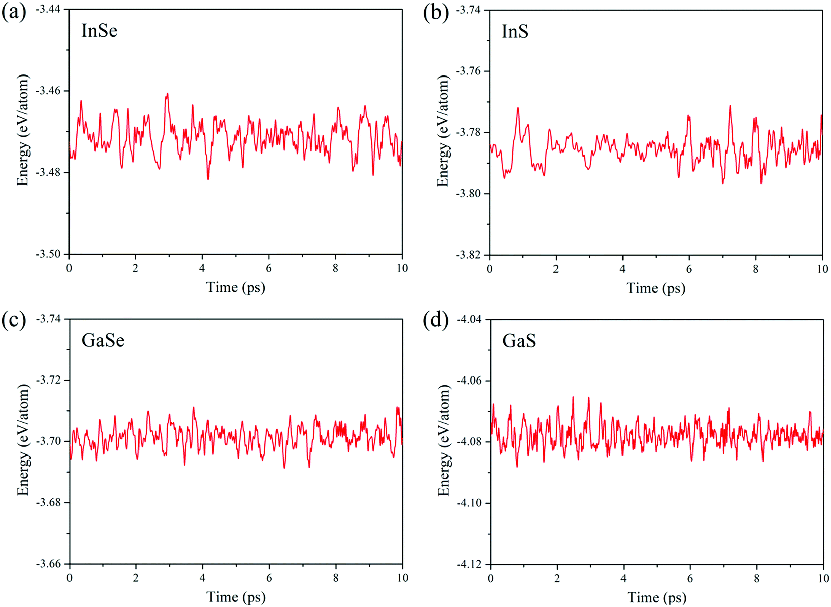 | ||
| Fig. 2 Fluctuations of the potential energies of monolayer C2h (a) InSe, (b) InS, (c) GaSe, and (d) GaS during the process of molecular dynamics under a temperature of 300 K. | ||
3.3. Electronic properties
Calculated electronic band structures at the HSE06 level are demonstrated in Fig. 3. The conduction band minima (CBM) and valence band maxima (VBM) for all monolayer C2h MXs occur at the Brillouin zone center (Γ symmetry point), indicating that all of them exhibit direct band gap characteristics. The energetic gaps of C2h monolayer InSe, InS, GaSe, and GaS are 2.38, 2.78, 2.39, and 2.84 eV respectively, located in the visible spectrum. Comparing the band gap of the single-layer C2h InSe to that of the bulk sample (a direct bandgap of 1.647 eV reported by Ghalouci et al.),34 a significant gap broadening of 0.73 eV is observed due to the quantum-confinement effect when the thickness of the material is down to the atomic level.22 This conclusion could be applied to other MXs as well.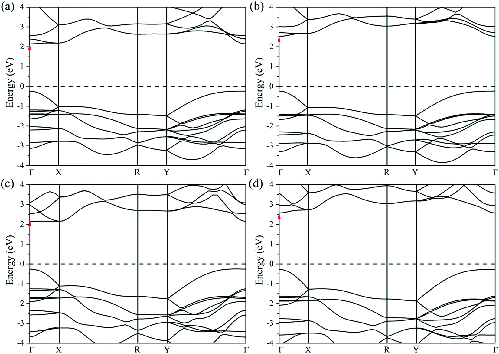 | ||
| Fig. 3 Computed electronic band structures of monolayer C2h (a) InSe, (b) InS, (c) GaSe, and (d) GaS at the HSE06 level. The red arrows point from VBM to CBM (direct band gaps at the Γ points). The values of the band gaps can be found in Table S1 (ESI†). | ||
As shown in Fig. 4 and Table S2 (ESI†), while the conduction band edge of D3h InSe monolayer has approximately equal contribution from In and Se (51.8% In and 48.2% Se), that of 2D C2h InSe is dominated by In (71.0% In and 29.0% Se). This finding can also be applied to the other three MX monolayers. Such different band-edge states in C2h MXs might give rise to exceptional electronic properties. It is also critical to emphasize that among all four single-layer MXs, C2h polymorph is the only phase that features a direct band gap, a property that the conventional D3h monolayers never possess. The origin of this extraordinary electronic property could be found in the band structures and the projected density of states (PDOS) diagrams. To begin with, just like what plenty of previous studies indicated, the single-layer D3h InSe features a non-parabolic “Mexican hat” shaped structure at the top of the valence band as shown in Fig. 4a.21,53 This unique band structure occurs when the material is thinned down from its bulk form to a single layer. The same “Mexican-hat” band edge occurs in other D3h MX monolayers as well, as shown in Fig. S5 (ESI†). The band structures of the bulk D3h MXs feature a direct band gap in which both the VBM and CBM locate at the Γ point, but during the process of thinning down, the top of the valence band at the Γ point shifts downward until it forms a double-peak shape.21,53 As a result, the VBM migrates away from the Γ point and converts the direct band into an indirect one. Such “Mexican hat” band structure of InSe results in a 2D van Hove singularity which is visible as a sudden peak of density of states right below the Fermi energy (Fig. 4a).53 Similar phenomena are observed in our calculated band structures for all monolayer D3h MXs besides InSe, and sudden increases in the density of states are found near the top of the valence bands, contributed mainly by the pz orbitals (shown in orange), according to our calculated PDOS diagrams (Fig. S5, ESI†). However, in comparison, the top of valence bands at the Γ points of the 2D C2h MXs remain parabolic in nature (Fig. 4): there is no “Mexican hat” structure at the top of the valence bands. Thus, the VBMs remain at the Γ points, and the direct band features are maintained. At the VBMs of the C2h monolayers, the PDOS's in Fig. 4 and Fig. S5 (ESI†) also reveal a lack of the sudden peak of density of states that is associated with the van Hove singularity in D3h monolayers. In fact, the PDOS diagrams unveil that there are still sudden increases in the density of states contributed by the pz orbitals in C2h MXs between about −1.3 to −1.8 eV as shown in Fig. 4 and Fig. S5 (ESI†). However, the pz orbitals are no longer dominating the top valence bands in C2h monolayers; instead, they are rather lower in energy compared to the px/y orbitals which now compose the topmost valence bands. The unique appearance of the latter in the C2h phase overshadows the influence of the “Mexican-hat” shaped band responsible for the direct–indirect transition in the 2D D3h polymorphs, and thus retains the direct band gap feature in the monolayer C2hMXs. We also consider the effect of spin–orbit coupling (SOC) on the electronic band structures (Fig. S6, ESI†). Small differences between the band structures with and without SOC indicate its weak and negligible influence.
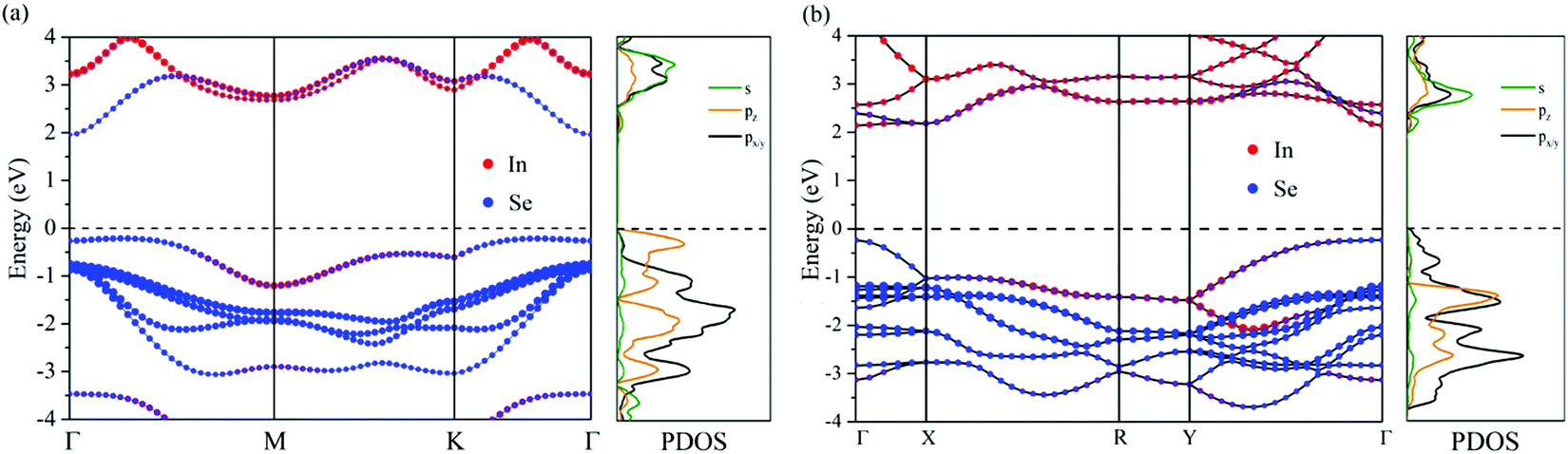 | ||
| Fig. 4 A close comparison between the projected band structures (computed at the HSE06 level) of monolayer (a) D3h and (b) C2h InSe. | ||
We also explore the transport properties of the 2D C2h MXs based on the ab initio Boltzmann transportation equation (BTE) method. Carrier mobilities of all four MX monolayers belonging to both D3h and C2h space groups are calculated and tabulated in Table 2; their corresponding effective masses are reported in Table S3 (ESI†). The validity of our computation is tested since our calculated room-temperature electron mobility of 2D D3h InSe (136 cm2 V−1 s−1) is similar to that reported in the study by Li et al. (120 cm2 V−1 s−1).54 According to Table 2, except for GaS, all four C2h MX monolayers exhibit higher electron mobilities along the y-direction compared to their corresponding D3h counterparts at 300 K. However, electron mobilities along the x-direction are comparatively lower in C2h MXs than in D3h monolayers, which can be attributed to the larger effective masses ( ) in the former ones, as shown in Table S3 (ESI†). For example, compared to the electron mobility of 2D D3h InSe (136 cm2 V−1 s−1) monolayer C2h InSe exhibits lower mobilities in the x-direction (23 cm2 V−1 s−1). Correspondingly, the electron effective mass along the x-direction in monolayer C2h InSe (0.743 m0) is higher than that in single-layer D3h InSe (0.190 m0), suggesting that it might be the heavier electron effective mass that results in a lower mobility. On the other hand, hole mobilities along both in-plane directions in 2D C2h MXs are prominently higher than those in the D3h phase. While hole mobilities along the y-direction (μh,y) in the C2h phase is about two to three times greater than those in the D3h monolayers (e.g., μh,y = 9.7 cm2 V−1 s−1 and 4.8 cm2 V−1 s−1 in C2h and D3h InSe, respectively), μh,x in the former phase could be up to one order of magnitude higher than those in the latter (e.g., μh,x = 67 cm2 V−1 s−1 and 4.8 cm2 V−1 s−1 in C2h and D3h InSe, respectively). This phenomenon could be explained by the much smaller densities of states near the valence band edges of the C2h monolayers, a parameter identified by Li et al.54 as the key factor influencing the hole mobility in 2D materials. As mentioned before, the “Mexican-hat” shaped valence band edge in a D3h monolayer MX gives rise to a sharp peak (van Hove singularity) in the density of states which increases the hole scattering rate, decreasing the carrier lifetime and the mobility. However, the lack of a similar peak in density of states associated with the van Hove singularity at the VBM of a C2h monolayer spares the holes from a high probability of scattering, thus extending the carrier lifetime and maintaining a high hole mobility. But what really makes C2h monolayers stand out is their strong anisotropic characteristic, featuring higher electron mobilities along the y-direction and higher hole mobilities along the x-direction. In other words, the dominant transport direction in monolayered C2h MXs exhibits a strong dependency on the carrier type. This property renders single-layer C2h MXs suitable materials in nanoelectronics devices in which the superior transport direction can be readily altered by a change of carriers induced by switching the sign of the applied gate voltage. The anisotropic transport property might be contributed by different effective masses of the carriers along x- and y-directions, as shown in Table S3 (ESI†). Take C2h InSe as an example. On one hand, while its hole effective mass along the y-direction is as high as 4.02 m0, that in the x-direction is approximately an order smaller, having a value of 0.304 m0. Correspondingly, the hole mobility in the x-direction (67 cm2 V−1 s−1) is almost one magnitude greater than that in the y-direction (9.7 cm2 V−1 s−1). On the other hand, a lower electron mobility along the x-direction (23 cm2 V−1 s−1 and 149 cm2 V−1 s−1 in the x- and y-direction respectively) corresponds to a larger effective mass (0.743 m0 and 0.216 m0 in the x- and y-direction respectively).
| μ e (cm2 V−1 s−1) | μ h (cm2 V−1 s−1) | ||||||||
|---|---|---|---|---|---|---|---|---|---|
| 100 K | 300 K | 100 K | 300 K | ||||||
| x | y | x | y | x | y | x | y | ||
| InSe | D 3h | 378 | 378 | 136 | 136 | 6.4 | 6.4 | 4.8 | 4.8 |
| C 2h | 134 | 528 | 23 | 149 | 239 | 21 | 67 | 9.7 | |
| InS | D 3h | 239 | 239 | 66 | 66 | 4.5 | 4.5 | 3.3 | 3.3 |
| C 2h | 856 | 885 | 64 | 186 | 533 | 25.8 | 120 | 10.6 | |
| GaSe | D 3h | 404 | 404 | 168 | 168 | 22 | 22 | 9 | 9 |
| C 2h | 397 | 859 | 39 | 180 | 372 | 123 | 65 | 20 | |
| GaS | D 3h | 421 | 421 | 209 | 209 | 3.9 | 3.9 | 2.2 | 2.2 |
| C 2h | 78 | 128 | 25 | 77 | 80 | 6.9 | 28 | 4.7 | |
3.4. Optical properties
The optical properties of C2h MXs monolayers are demonstrated and compared to those of their corresponding conventional D3h polymorphs in their optical absorption spectra along x- and y-directions as shown in Fig. 5. Prominent optical absorption coefficients (on the order of 105 cm−1) are observed in all C2h MXs monolayers in the range of visible-UV lights. Especially when comparing the x-direction absorption spectra of C2h (orange curves in Fig. 5) and D3h (green curves in Fig. 5) MXs, the former exhibits significantly stronger absorption of visible and near-ultraviolet light than the latter does (approximately two times the latter in the range of 2 to 3 eV), implying a higher utilization efficiency of solar energy in C2h MXs. The absorption spectra (Fig. 5) also indicate the conspicuously anisotropic optical characteristics of 2D C2h MXs materials which are never found in their traditional D3h phases. More specifically, along the x-direction of 2D C2h MXs (orange curves in Fig. 5), absorption is much stronger in the visible and the near-ultraviolet but is significantly weaker as the energy further increases in the ultraviolet range when compared to that in the y-direction (black curves in Fig. 5). This intrinsic optical anisotropy of C2h MXs monolayers endows themselves with promising potential for anisotropic optoelectronic applications.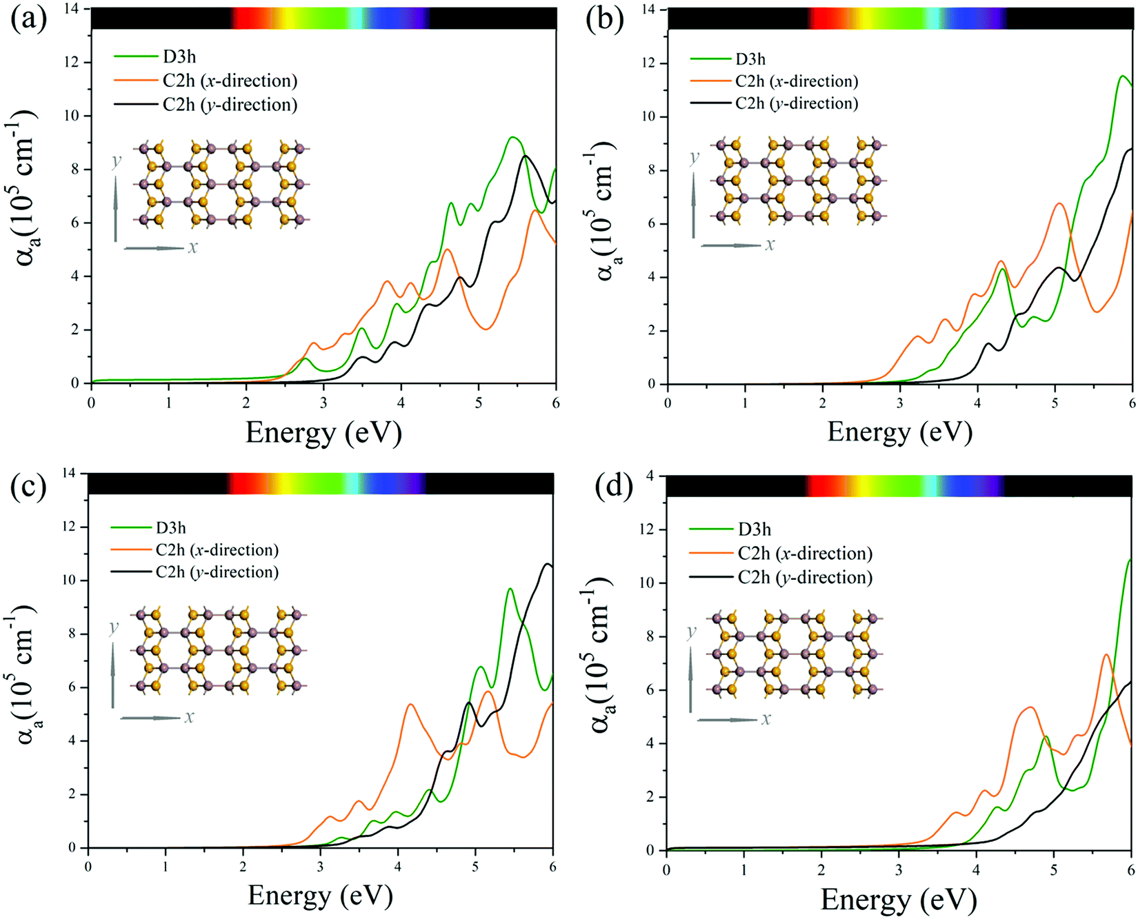 | ||
| Fig. 5 Calculated absorption coefficients (αa) in monolayer (a) InSe, (b) InS, (c) GaSe, and (d) GaS. The isotropic absorption coefficients of the D3h phases are shown in green. For the C2h monolayers, the absorption coefficients along the x-direction are shown in orange and those along the y-direction are shown in black. The insets show the two in-plane directions with respect to the top view of the C2h structure. | ||
4. Conclusions
To summarize, properties of single-layer C2h group III monochalcogenides are predicted. We identified the stable 2D C2h polymorph via global structural searches based on the particle swarm optimization algorithm. Notably, first-principles investigations on the electronic structures indicate that all C2h monolayer MXs feature a wide direct bandgap ranging from 2.38 to 2.84 eV, a property that the conventional D3h phase does not possess. In addition, carrier mobilities in C2h monolayers are found to be anisotropic and higher in magnitude compared to their D3h counterparts. Moreover, anisotropic and strong optical absorption ability in the order of 105 cm−1 is observed in the visible to ultraviolet region, indicating a high utilization efficiency of solar energy. All these excellent properties render the C2h MXs monolayers potential candidates for future high efficiency solar cells and optoelectronics.Conflicts of interest
There are no conflicts to declare.Acknowledgements
We are grateful for the financial support from SUSTech startup fund (Y01216143) and Guangdong Basic and Applied Basic Research Foundation (2021A1515010387). Computational work was supported by Center for Computational Science and Engineering at Southern University of Science and Technology. The calculations were also performed by using the CHEM high-performance supercomputer cluster (CHEM-HPC) located at department of chemistry, SUSTech. We thank Prof. Qihang Liu (SUSTech) and Dr. Xiao Wang (Shenzhen Institute of Advanced Technology, Chinese Academy of Sciences) for helpful discussions.References
- K. Novoselov, Electric Field Effect in Atomically Thin Carbon Films, Science, 2004, 306, 666–669 CrossRef CAS PubMed.
- A. Geim and K. Novoselov, The Rise of Graphene, Nat. Mater., 2007, 6, 183–191 CrossRef CAS PubMed.
- F. Xia, H. Wang, D. Xiao, M. Dubey and A. Ramasubramaniam, Two-Dimensional Material Nanophotonics, Nat. Photonics, 2014, 8, 899–907 CrossRef CAS.
- D. Akinwande, N. Petrone and J. Hone, Two-Dimensional Flexible Nanoelectronics, Nat. Commun., 2014, 5, 1–12 Search PubMed.
- H. Zhao, Q. Guo, F. Xia and H. Wang, Two-Dimensional Materials for Nanophotonics Application, Nanophotonics, 2015, 4, 128–142 Search PubMed.
- M. Chhowalla, D. Jena and H. Zhang, Two-Dimensional Semiconductors for Transistors, Nat. Rev. Mater., 2016, 1, 1–15 Search PubMed.
- Y. Liu, X. Duan, Y. Huang and X. Duan, Two-Dimensional Transistors Beyond Graphene and TMDCs, Chem. Soc. Rev., 2018, 47, 6388–6409 RSC.
- S. Cahangirov, M. Topsakal, E. Aktürk, H. Şahin and S. Ciraci, Two-and One-Dimensional Honeycomb Structures of Silicon and Germanium, Phys. Rev. Lett., 2009, 102, 236804 CrossRef CAS PubMed.
- J. Garcia, D. de Lima, L. Assali and J. Justo, Group IV Graphene-and Graphane-Like Nanosheets, J. Phys. Chem. C, 2011, 115, 13242–13246 CrossRef CAS.
- H. Şahin, S. Cahangirov, M. Topsakal, E. Bekaroglu, E. Akturk, R. Senger and S. Ciraci, Monolayer Honeycomb Structures of Group-IV Elements and III-V Binary Compounds: First-Principles Calculations, Phys. Rev. B: Condens. Matter Mater. Phys., 2009, 80, 155453 CrossRef.
- K. Chang and S. Parkin, Experimental Formation of Monolayer Group-IV Monochalcogenides, J. Appl. Phys., 2020, 127, 220902 CrossRef CAS.
- L. Xu, M. Yang, S. Wang and Y. Feng, Electronic and Optical Properties of the Monolayer Group-IV Monochalcogenides MX (M = Ge, Sn; X = S, Se, Te), Phys. Rev. B, 2017, 95, 235434 CrossRef.
- Q. Wang, K. Kalantar-Zadeh, A. Kis, J. Coleman and M. Strano, Electronics and Optoelectronics of Two-Dimensional Transition Metal Dichalcogenides, Nat. Nanotechnol., 2012, 7, 699–712 CrossRef CAS PubMed.
- D. Jariwala, V. Sangwan, L. Lauhon, T. Marks and M. Hersam, Emerging Device Applications for Semiconducting Two-Dimensional Transition Metal Dichalcogenides, ACS Nano, 2014, 8, 1102–1120 CrossRef CAS PubMed.
- L. Li, Y. Yu, G. Ye, Q. Ge, X. Ou, H. Wu, D. Feng, X. Chen and Y. Zhang, Black Phosphorus Field-Effect Transistors, Nat. Nanotechnol., 2014, 9, 372–377 CrossRef CAS PubMed.
- X. Ling, H. Wang, S. Huang, F. Xia and M. Dresselhaus, The Renaissance of Black Phosphorus, Proc. Natl. Acad. Sci. U. S. A., 2015, 112, 4523–4530 CrossRef CAS PubMed.
- D. Bandurin, A. Tyurnina, G. Yu, A. Mishchenko, V. Zólyomi, S. Morozov, R. Kumar, R. Gorbachev, Z. Kudrynskyi, S. Pezzini, Z. Kovalyuk, U. Zeitler, K. Novoselov, A. Patanè, L. Eaves, I. Grigorieva, V. Fal'ko, A. Geim and Y. Cao, High Electron Mobility, Quantum Hall Effect and Anomalous Optical Response in Atomically Thin InSe, Nat. Nanotechnol., 2016, 12, 223–227 CrossRef PubMed.
- C. Ren, S. Wang, H. Tian, Y. Luo, J. Yu, Y. Xu and M. Sun, First-Principles Investigation on Electronic Properties and Band Alignment of Group III Monochalcogenides, Sci. Rep., 2019, 9, 1–6 Search PubMed.
- S. Demirci, N. Avazlı, E. Durgun and S. Cahangirov, Structural and Electronic Properties of Monolayer Group III Monochalcogenides, Phys. Rev. B, 2017, 95, 115409 CrossRef.
- G. Mudd, M. Molas, X. Chen, V. Zólyomi, K. Nogajewski, Z. Kudrynskyi, Z. Kovalyuk, G. Yusa, O. Makarovsky, L. Eaves, M. Potemski, V. Fal’ko and A. Patanè, The Direct-to-Indirect Band Gap Crossover in Two-Dimensional van der Waals Indium Selenide Crystals, Sci. Rep., 2016, 6, 1–10 CrossRef PubMed.
- W. Feng, W. Zheng, W. Cao and P. Hu, Back Gated Multilayer InSe Transistors with Enhanced Carrier Mobilities via the Suppression of Carrier Scattering from a Dielectric Interface, Adv. Mater., 2014, 26, 6587–6593 CrossRef CAS PubMed.
- G. Mudd, S. Svatek, T. Ren, A. Patanè, O. Makarovsky, L. Eaves, P. Beton, Z. Kovalyuk, G. Lashkarev, Z. Kudrynskyi and A. Dmitriev, Tuning the Bandgap of Exfoliated InSe Nanosheets by Quantum Confinement, Adv. Mater., 2013, 25, 5714–5718 CrossRef CAS PubMed.
- S. Shi, Z. Sun and Y. Hu, Synthesis, Stabilization and Applications of 2-Dimensional 1T Metallic MoS2, J. Mater. Chem. A, 2018, 6, 23932–23977 RSC.
- X. Li and H. Zhu, Two-Dimensional MoS2: Properties, Preparation, and Applications, J. Materiomics, 2015, 1, 33–44 CrossRef.
- Z. Zhu and D. Tománek, Semiconducting layered blue phosphorus: a computational study, Phys. Rev. Lett., 2014, 112, 176802 CrossRef PubMed.
- P. Hu, Z. Wen, L. Wang, P. Tan and K. Xiao, Synthesis of Few-Layer GaSe Nanosheets for High Performance Photodetectors, ACS Nano, 2012, 6, 5988–5994 CrossRef CAS PubMed.
- P. Hu, L. Wang, M. Yoon, J. Zhang, W. Feng, X. Wang, Z. Wen, J. Idrobo, Y. Miyamoto, D. Geohegan and K. Xiao, Highly Responsive Ultrathin GaS Nanosheet Photodetectors on Rigid and Flexible Substrates, Nano Lett., 2013, 13, 1649–1654 CrossRef CAS PubMed.
- Z. Yang, W. Jie, C. Mak, S. Lin, H. Lin, X. Yang, F. Yan, S. Lau and J. Hao, Wafer-Scale Synthesis of High-Quality Semiconducting Two-Dimensional Layered InSe with Broadband Photoresponse, ACS Nano, 2017, 11, 4225–4236 CrossRef CAS PubMed.
- W. Li, S. Poncé and F. Giustino, Dimensional crossover in the carrier mobility of two-dimensional semiconductors: the case of InSe, Nano Lett., 2019, 19, 1774–1781 CrossRef CAS PubMed.
- H. Zhuang and R. Hennig, Single-Layer Group-III Monochalcogenide Photocatalysts for Water Splitting, Chem. Mater., 2013, 25, 3232–3238 CrossRef CAS.
- Y. Sun, Y. Li, T. Li, K. Biswas, A. Patanè and L. Zhang, New Polymorphs of 2D Indium Selenide with Enhanced Electronic Properties, Adv. Funct. Mater., 2020, 30, 2001920 CrossRef CAS PubMed.
- J. Grzonka, M. Claro, A. Molina-Sánchez, S. Sadewasser and P. Ferreira, Novel Polymorph of GaSe, Adv. Funct. Mater., 2021, 2104965 CrossRef CAS.
- K. Cenzual, L. Gelato, M. Penzo and E. Parthé, Inorganic Structure Types with Revised Space Groups. I, Acta Crystallogr., Sect. B: Struct. Sci., 1991, 47, 433–439 CrossRef.
- L. Ghalouci, F. Taibi, F. Ghalouci and M. Bensaid, Ab Initio Investigation into Structural, Mechanical and Electronic Properties of Low Pressure, High Pressure and High Pressure-High Temperature Phases of Indium Selenide, Comput. Mater. Sci., 2016, 124, 62–77 CrossRef CAS.
- D. Errandonea, D. Martínez-García, A. Segura, A. Chevy, G. Tobias, E. Canadell and P. Ordejon, High-Pressure, High-Temperature Phase Diagram of InSe: A Comprehensive Study of the Electronic and Structural Properties of the Monoclinic Phase of InSe under High Pressure, Phys. Rev. B: Condens. Matter Mater. Phys., 2006, 73, 235202 CrossRef.
- Y. Wang, J. Lv, L. Zhu and Y. Ma, CALYPSO: A Method for Crystal Structure Prediction, Comput. Phys. Commun., 2012, 183, 2063–2070 CrossRef CAS.
- G. Kresse and J. Hafner, Ab Initio Molecular Dynamics for Liquid Metals, Phys. Rev. B: Condens. Matter Mater. Phys., 1993, 47, 558–561 CrossRef CAS PubMed.
- G. Kresse and J. Furthmüller, Efficiency of Ab-Initio Total Energy Calculations for Metals and Semiconductors Using a Plane-Wave Basis Set, Comput. Mater. Sci., 1996, 6, 15–50 CrossRef CAS.
- G. Kresse and J. Furthmüller, Efficient Iterative Schemes Forab Initiototal-Energy Calculations Using a Plane-Wave Basis Set, Phys. Rev. B: Condens. Matter Mater. Phys., 1996, 54, 11169–11186 CrossRef CAS PubMed.
- G. Kresse and J. Hafner, Ab Initio Molecular-Dynamics Simulation of the Liquid-Metal–Amorphous-Semiconductor Transition in Germanium, Phys. Rev. B: Condens. Matter Mater. Phys., 1994, 49, 14251–14269 CrossRef CAS PubMed.
- G. Martyna, M. Klein and M. Tuckerman, Nosé–Hoover Chains: The Canonical Ensemble Via Continuous Dynamics, J. Chem. Phys., 1992, 97(4), 2635–2643 CrossRef.
- P. Giannozzi, S. Baroni, N. Bonini, M. Calandra, R. Car, C. Cavazzoni, D. Ceresoli, G. Chiarotti, M. Cococcioni, I. Dabo, A. Dal Corso, S. de Gironcoli, S. Fabris, G. Fratesi, R. Gebauer, U. Gerstmann, C. Gougoussis, A. Kokalj, M. Lazzeri, L. Martin-Samos, N. Marzari, F. Mauri, R. Mazzarello, S. Paolini, A. Pasquarello, L. Paulatto, C. Sbraccia, S. Scandolo, G. Sclauzero, A. Seitsonen, A. Smogunov, P. Umari and R. Wentzcovitch, QUANTUM ESPRESSO: A Modular And Open-Source Software Project For Quantum Simulations Of Materials, J. Phys.: Condens. Matter, 2009, 21(39), 395502 CrossRef PubMed.
- P. Giannozzi, O. Andreussi, T. Brumme, O. Bunau, M. Buongiorno Nardelli, M. Calandra, R. Car, C. Cavazzoni, D. Ceresoli, M. Cococcioni, N. Colonna, I. Carnimeo, A. Dal Corso, S. de Gironcoli, P. Delugas, R. DiStasio, A. Ferretti, A. Floris, G. Fratesi, G. Fugallo, R. Gebauer, U. Gerstmann, F. Giustino, T. Gorni, J. Jia, M. Kawamura, H. Ko, A. Kokalj, E. Küçükbenli, M. Lazzeri, M. Marsili, N. Marzari, F. Mauri, N. Nguyen, H. Nguyen, A. Otero-de-la-Roza, L. Paulatto, S. Poncé, D. Rocca, R. Sabatini, B. Santra, M. Schlipf, A. Seitsonen, A. Smogunov, I. Timrov, T. Thonhauser, P. Umari, N. Vast, X. Wu and S. Baroni, Advanced capabilities for materials modelling with Quantum ESPRESSO, J. Phys.: Condens. Matter, 2017, 29(46), 465901 CrossRef CAS PubMed.
- P. Giannozzi, O. Baseggio, P. Bonfà, D. Brunato, R. Car, I. Carnimeo, C. Cavazzoni, S. de Gironcoli, P. Delugas, F. Ferrari Ruffino, A. Ferretti, N. Marzari, I. Timrov, A. Urru and S. Baroni, Quantum Espresso Toward the Exascale, J. Chem. Phys., 2020, 152(15), 154105 CrossRef CAS PubMed.
- J. Perdew, K. Burke and M. Ernzerhof, Generalized Gradient Approximation Made Simple, Phys. Rev. Lett., 1996, 77, 3865–3868 CrossRef CAS PubMed.
- J. Perdew, K. Burke and M. Ernzerhof, Generalized Gradient Approximation Made Simple, Phys. Rev. Lett., 1997, 78, 1396 CrossRef CAS.
- P. Blöchl, Projector Augmented-Wave Method, Phys. Rev. B: Condens. Matter Mater. Phys., 1994, 50, 17953–17979 CrossRef PubMed.
- G. Kresse and D. Joubert, From Ultrasoft Pseudopotentials to the Projector Augmented-Wave Method, Phys. Rev. B: Condens. Matter Mater. Phys., 1999, 59, 1758–1775 CrossRef CAS.
- J. Paier, M. Marsman, K. Hummer, G. Kresse, I. Gerber and J. Ángyán, Screened Hybrid Density Functionals Applied to Solids, J. Chem. Phys., 2006, 124, 154709 CrossRef CAS PubMed.
- S. Poncé, E. Margine, C. Verdi and F. Giustino, EPW: Electron–Phonon Coupling, Transport and Superconducting Properties Using Maximally Localized Wannier Functions, Comput. Phys. Commun., 2016, 209, 116–133 CrossRef.
- F. Giustino, Electron-Phonon Interactions from First Principles, Rev. Mod. Phys., 2017, 89, 015003 CrossRef.
- H. Shu, F. Li, C. Hu, P. Liang, D. Cao and X. Chen, The Capacity Fading Mechanism and Improvement of Cycling Stability in MoS2-Based Anode Materials for Lithium-Ion Batteries, Nanoscale, 2016, 8, 2918–2926 RSC.
- H. Cai, Y. Gu, Y. Lin, Y. Yu, D. Geohegan and K. Xiao, Synthesis and Emerging Properties of 2D Layered III–VI Metal Chalcogenides, Appl. Phys. Rev., 2019, 6, 041312 Search PubMed.
- W. Li, S. Poncé and F. Giustino, Dimensional Crossover in the Carrier Mobility of Two-Dimensional Semiconductors: the Case of InSe, Nano Lett., 2019, 19, 1774–1781 CrossRef CAS PubMed.
Footnotes |
| † Electronic supplementary information (ESI) available. See DOI: 10.1039/d1ma01068a |
| ‡ These authors contributed equally to this work. |
| This journal is © The Royal Society of Chemistry 2022 |