
 Open Access Article
 This Open Access Article is licensed under a Creative Commons Attribution-Non Commercial 3.0 Unported Licence
Facet-dependent carrier dynamics of cuprous oxide regulating the photocatalytic hydrogen generation†
Cui Ying
Toe
 a,
Marlene
Lamers
b,
Thomas
Dittrich
c,
Hassan A.
Tahini
d,
Sean C.
Smith
d,
Jason
Scott
a,
Rose
Amal
a,
Roel
van de Krol
b,
Fatwa F.
Abdi
*b and
Yun Hau
Ng
*ae
a,
Marlene
Lamers
b,
Thomas
Dittrich
c,
Hassan A.
Tahini
d,
Sean C.
Smith
d,
Jason
Scott
a,
Rose
Amal
a,
Roel
van de Krol
b,
Fatwa F.
Abdi
*b and
Yun Hau
Ng
*ae
aParticles and Catalysis Research Group, School of Chemical Engineering, The University of New South Wales, NSW 2052, Australia. E-mail: yunhau.ng@cityu.edu.hk
bInstitute for Solar Fuels, Helmholtz-Zentrum Berlin für Materialien und Energie GmbH, Hahn-Meitner-Platz 1, Berlin 14109, Germany
cInstitute for Silicon Photovoltaics, Helmholtz-Zentrum Berlin für Materialien und Energie GmbH, Kekuléstrasse 5, Berlin 12489, Germany
dResearch School of Physics and Engineering, The Australian National University, Canberra, ACT 2601, Australia
eSchool of Energy and Environment, City University of Hong Kong, Kowloon, Hong Kong SAR, P. R. China
First published on 21st January 2022
Abstract
The intrinsic carrier dynamics of cuprous oxide (Cu2O) are known to have a crucial influence on photocatalytic performances. The photoactivity of rhombic dodecahedral Cu2O with dominant {110} facets (RD-Cu2O) is demonstrated to surpass that of cubic Cu2O with {100} surfaces (CB-Cu2O). Time resolved microwave conductivity (TRMC) measurements reveal the higher carrier mobility of RD-Cu2O when compared to CB-Cu2O. Additionally, modulated surface photovoltage (SPV) measurements further supported the better charge separation efficiency of RD-Cu2O. Although CB-Cu2O exhibited more pronounce SPV signals, the homogeneous distribution of electrical fields drives the majority charge inward and led to detrimental charge recombination. In contrast, the weak SPV signals for RD-Cu2O were attributed to a modulated distribution of charges towards the facets and facet boundaries, demonstrating a better charge separation. This study shows that carrier dynamics and defect density should also be regarded as facet-dependent properties that can have deciding influence on the photocatalytic activity.
1. Introduction
Morphology control through crystal facet engineering has attracted significant attention due to its ability to optimize the performance of various photocatalysts.1 Given the unique facet-dependent properties, rapid advancements have been made in the synthesis of crystalline functional materials (both semiconductor and metal) with well-defined facets such as bismuth-based ternary oxides (e.g. BiVO4 and Bi2WO6), TiO2, Cu2O, CdSe, Au and Ag.2–7 Formation of distinctive crystal facets motivated numerous morphological studies that demonstrated enhanced reactivity and selectivity. Apart from the activity enhancement, tailoring the extent of facet exposure has also enabled the determination of specific oxidation and reduction sites on a photocatalyst. Photoreduction of Pt6+ to Pt and photooxidation of Pb2+ to PbO2 were first discovered to specifically occur on (110) and (011) facets of TiO2, respectively.8 Similar technique has also been employed to reveal the active photoreduction and oxidation sites of BiVO4,2,9 BiOCl10 and BiOBr.11 Most of the crystal facet investigations, however, focused on n-type photocatalysts and little is known about the reactivity of different facets of p-type materials.Inspired by the above-mentioned progress in facet engineering, recent studies have shown that Cu2O with different exposed crystal planes also show facet-dependent properties manifested by its distinct photoreactivity. Cu2O has emerged as an attractive p-type semiconductor for both photocatalytic and photoelectrochemical water splitting due to its favorable electronic structure that is suitable for solar energy harvesting (i.e. bandgap of ∼2.0 eV with a conduction band potential more negative than the water reduction potential).12 Architecture control of Cu2O is also one of the promising research areas owing to its ease in forming numerous morphologies such as spheres,13 plates,14 flower-like,15 cubes,16 nanowires,17 nanocages18,19 and various polyhedrons,20 and its capability of being used as a template to fabricate various well-defined hollow structures.21 Xu and Xue demonstrated gradual evolutions of Cu2O shapes with well-developed facets via reduction based on five branching growth patterns.15 Organic and inorganic additives (e.g. PVP, CTAB, steric acid, oleic acid and KI) have also been employed as selective surface stabilizers during synthesis to control Cu2O growth.14,16,20,22–24
The common perspective used to explain photoreactivity variations of Cu2O with different exposed facets are (1) surface atomic arrangement resulting in altered adsorption abilities of reactant/product and (2) surface potential-dependent surface electronic band structures.25–28 For instance, the high-performing Cu2O with {110} exposed facet is known to have higher concentrations of copper dangling bonds and favorable surface potentials.20 Chu and Huang also demonstrated the best performance of rhombic dodecahedral Cu2O attributed to its ideal surface electronic structure.29 To date, various attempts have been devoted to elucidating energy level-shifts of Cu2O with distinctive facets through both modelling and experimental approaches. The former involved density functional theory (DFT) calculations while the latter involved the approximation of band structures using techniques such as UV-Vis, X-ray photoelectron spectroscopy (XPS), ultraviolet photoelectron spectroscopy (UPS) and Mott–Schottky measurements to determine bandgaps, Fermi levels and surface potentials. Due to the complexity in performing direct experimental comparisons of surface adsorption abilities and surface potentials, these parameters are often predicted via density functional theory (DFT) calculations. From a surface electronic structure view point, the shift in surface potentials is believed to affect the dynamics of the charge carriers, such as carrier mobility, lifetime and diffusion length. However, little effort has been invested in evaluating the intrinsic charge dynamic differences of faceted photocatalysts, particularly Cu2O. In addition to affecting the surface electronic structures, defects that are incorporated within the materials can also have significant influence on the intrinsic carrier dynamics. For instance, oxygen vacancies were introduced into SrTiO3 photocatalyst in reducing atmosphere with low oxygen partial pressure and was shown to induce electron doping, which increases the electron density. The oxygen vacancy density was also quantifiable based on the change in electron density.30 Given the commonly used approach to tailor the exposed crystal facets by varying synthesis conditions (e.g. temperature and concentration of precursors/additives), deviations in surface chemistry across samples are unavoidable. As a result, changes to defect concentrations that subsequently modulate intrinsic carrier dynamics are often observed.
Local charge separation plays a decisive role in photocatalysis. For example, local charge separation across microcrystals of BiVO4 was found to be strongly stimulated by facet-selective deposition of cocatalysts and led to a strong increase of oxygen evolution.31 Furthermore, Chen et al. has also shown that a dedicated variation of the local defect structure of cubic Cu2O microcrystals led to opposite directions of charge separation at a single facet of a Cu2O microcrystal.32 In order to attain a comprehensive understanding of carrier dynamic differences, we employ time-resolved microwave conductivity (TRMC) measurements to evaluate effective carrier mobility, lifetime and diffusion length.33 In addition, modulated surface photovoltage (SPV) measurements are used to assess the spatial separation mechanism of photogenerated charges and their relaxation. The relaxation can last over many orders of magnitude in time, mainly due to transport limitations over barriers and/or trapping.34 Therefore, modulated SPV provides complementary information to methods that are only sensitive to free charge carriers, such as TRMC.
Although Cu2O surface electronic structures that are interrelated to its intrinsic carrier dynamics have been computed via DFT calculations, experimental verifications of these intrinsic properties play an equally important role to eliminate the possible discrepancies between modelled and actual samples. In this work, cubic and rhombic dodecahedral Cu2O with dominant exposed {100} and {110} facets, respectively, were employed to understand the influence of facet-dependent properties to their photoactivity. The prominent photoactivity of rhombic dodecahedral Cu2O in conjunction with its enhanced charge carrier mobility and charge separation signifies the strong influence of carrier dynamics as one of the facet-dependent properties. This work pioneers the experimental investigation on Cu2O carrier dynamic influence towards photoactivity.
2. Results and discussions
2.1. Photocatalytic performance
Two Cu2O batches with distinct morphologies were fabricated using a facile solution-phase method adapted from Liang et al.5 While the surfactant-free synthesis conditions produce uniform cubic Cu2O particles (Fig. 1a), the addition of oleic acid as the face-selective adsorption additive favors the growth of rhombic dodecahedral Cu2O (Fig. 1c). Observation of the samples at high magnification under a scanning electron microscope (SEM) shows that both samples exhibit a smooth surface as illustrated in Fig. 1b and d. Herein, the cubic Cu2O particles with six exposed {100} facets and the rhombic dodecahedral Cu2O particles dominantly enclosed by twelve {110} facets are denoted as CB-Cu2O and RD-Cu2O, respectively. Note that CB-Cu2O with sharp edges contains only one type of facet, while RD-Cu2O appears to have other small exposed facets at the corners (i.e. {100} facets) of the particles, as illustrated in Fig. 1d. Despite having distinct exposed facets, CB-Cu2O and RD-Cu2O show the same X-ray diffraction (XRD) peaks (Fig. 1e), which correspond to the cubic phase of Cu2O. The narrow and intense XRD peaks indicate that the two samples have similarly good crystallinity. As inferred by Scherrer's equation, the crystallite sizes were calculated to be 59 nm for CB-Cu2O and 70 nm for RD-Cu2O. Likewise, both samples display comparable absorption band edges at wavelengths of 615 and 620 nm, as illustrated in their UV-Vis diffuse reflectance spectra (Fig. 1f). The UV-Vis results indicate that CB-Cu2O and RD-Cu2O have a bandgap energy of 2.02 and 2.00 eV, respectively, consistent with that reported in the literature.35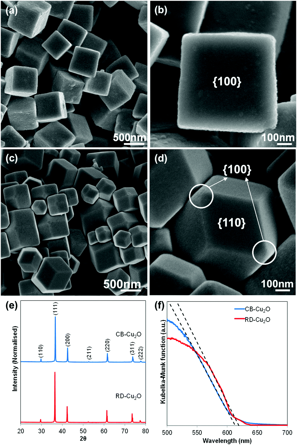 | ||
| Fig. 1 SEM images of (a and b) cubic Cu2O with dominant {100} facet, (c and d) rhombic dodecahedral Cu2O with dominant {110} facet, (e) XRD patterns and (f) UV-Vis absorption spectra of CB-Cu2O and RD-Cu2O converted using Kubelka–Munk transformation. | ||
The photoactivity of CB-Cu2O and RD-Cu2O was compared using photocatalytic (PC) and photoelectrochemical (PEC) approaches. In the PC system, the Cu2O particles were used to induce the reduction of water (i.e. hydrogen (H2) evolution) in an aqueous sodium sulfite (Na2SO3) solution. Upon excitation of Cu2O, the photoinduced holes are effectively scavenged by SO32− ions, whereas the photogenerated electrons reduce water to produce gaseous H2. As shown in Fig. 2a, a steady evolution of H2 was observed from both CB-Cu2O and RD-Cu2O. Careful examination shows that the amount of H2 produced after 6 h of irradiation for RD-Cu2O with exposed {110} facets (i.e. 29.6 μmol) clearly surpasses that of CB-Cu2O with exposed {100} facets (i.e. 19.5 μmol). H2 was not detected from the control experiments performed in the absence of light, indicating minimal effect of mechanical stirring during the reaction. Comparison of the H2 generation performance with literatures also shows that the performance is comparable to most of the existing pristine Cu2O systems (Table S1, ESI†). In addition, CB-Cu2O and RD-Cu2O powders were also made into photoelectrodes. The samples were separately drop-casted onto a conducting FTO substrate to obtain films with a particle density of 2 mg cm−2. Fig. 2b displays the photocurrent generated by CB-Cu2O and RD-Cu2O vs. time under chopped illumination, at a constant applied bias of 0.25 V vs. RHE. The cathodic photocurrents suggest that both CB-Cu2O and RD-Cu2O are p-type semiconductors. Unambiguously, RD-Cu2O exhibits a higher cathodic photocurrent than that of CB-Cu2O. Although there exist differences between PC and PEC systems,36,37 the significantly enhanced photoactivity of RD-Cu2O in both systems suggests that exposure of both {110} and {100} facets on Cu2O is beneficial when compared to only {100} facets. This is also in agreement with other reported literature that demonstrated better photoactivity of {110} facets when compared to {100} facets.25,26
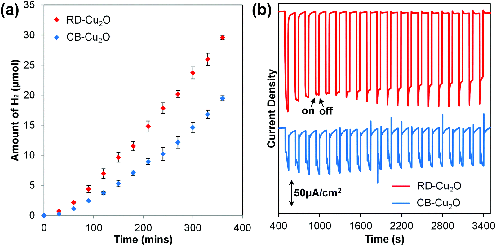 | ||
| Fig. 2 (a) Time course of photocatalytic H2 evolution during 6 hours of illumination and (b) PEC amperometric photocurrent densities of CB-Cu2O and RD-Cu2O. | ||
The attention is now shifted to the factors that influence the observed facet-dependent photoactivity of Cu2O. Both the bulk and surface properties of a semiconductor are known to influence the photoactivity.38,39 Since XRD and diffuse reflectance UV-Vis spectroscopy analyses show that CB-Cu2O and RD-Cu2O have a similar crystal structure, crystallinity and bandgap energy, the influence of these properties in determining the photoactivity can be disregarded. The possible contribution of different specific surface area can also be eliminated given that the better-performing RD-Cu2O has a BET surface area of 1.6 m2 g−1, which is half of that of CB-Cu2O (3.2 m2 g−1). Therefore, the different photoactivity of CB-Cu2O and RD-Cu2O in PC H2 evolution and PEC photocurrent generation can be attributed to the difference in the exposed facets. Several factors have been recently demonstrated to be dependent on the types of exposed facets: (1) the corrosion tendency, (2) the surface adsorption ability that relies on the surface atomic arrangement and (3) the charge transfer efficiency that is known to be affected by the variation of the surface electronic structure.40 Our previous work revealed that the dominant photocorrosion pathway for Cu2O in a PC system is self-photooxidation into CuO.41 In that study, we showed that the presence of a strong hole scavenger (i.e. Na2SO3) has not only improved the photocatalytic H2 evolution rate, photocorrosion of Cu2O has also been efficiently suppressed due to the rapid consumption of photogenerated holes that could otherwise be consumed for self-oxidation of Cu2O. Given that Na2SO3 was employed as a sacrificial reagent in this work, the difference in the corrosion tendencies between the two Cu2O samples with distinct exposed facets can be assumed to be minimal. The stability of the samples has also been tested with detailed information provided in the Fig. S1 (ESI†). As illustrated in Fig. S1c (ESI†), the performance of RD-Cu2O was retained at more than 80% after the third cycle of reaction.
2.2. Surface atomic structure
DFT calculations were employed to model the Cu2O {100} and {110} surfaces, as analogues to CB-Cu2O and RD-Cu2O facets, respectively. These surfaces can host a number of defects arising from their distinct surface features. These have been modelled and characterized extensively by Soon et al.,42 in which their surface nomenclatures for assigning surface defects are followed here. Each surface can exist with several different terminations (Cu, O and CuO), along with a number of native surface defects such as Cu or O vacancies and interstitials. Fig. 3a shows the atomic models of surfaces that were chosen from a set of structures with the lowest surface free energies within the range of experimentally achievable oxygen chemical pressure.42 The adsorption energies of H, H2 and H2O were obtained at different surface sites (Fig. 3b), with no clear trend observed. In general, H shows a strong preference to bind on O sites compared to Cu sites. In some cases, H binding energies are comparable, as illustrated by Cu2O{100}O and Cu2O{110}CuO-Cucsa@O sites (−2.24 eV and −2.41 eV, respectively). On the other hand, H2 binding is less sensitive to the surface details and binds with similar strengths on Cu and O sites. The difficulty to experimentally distinguish the existence of various surface terminations under ambient conditions complicates the comparison of surface adsorption abilities. One can assume that the two surfaces with relatively similar surface free energies will coexist. Hence, the adsorption abilities of H, H2 and H2O should not be very different from CB-Cu2O and RD-Cu2O. The above explanation is based on the adsorbate binding energies (Fig. 3b) obtained in the low coverage regime. At high coverages where all active sites are occupied, the H* free energy of Cu2O{110}CuO surface (−0.3 eV) is relatively closer to the ideal adsorption energy of 0 eV, when compared to −1.85 eV and −1.77 eV for Cu2O{100}O and Cu2O{110}CuO-Cucsa@O, respectively (Fig. S2, ESI†). This indirectly indicates a better adsorption of H* on RD-Cu2O with high H2 evolution efficiency.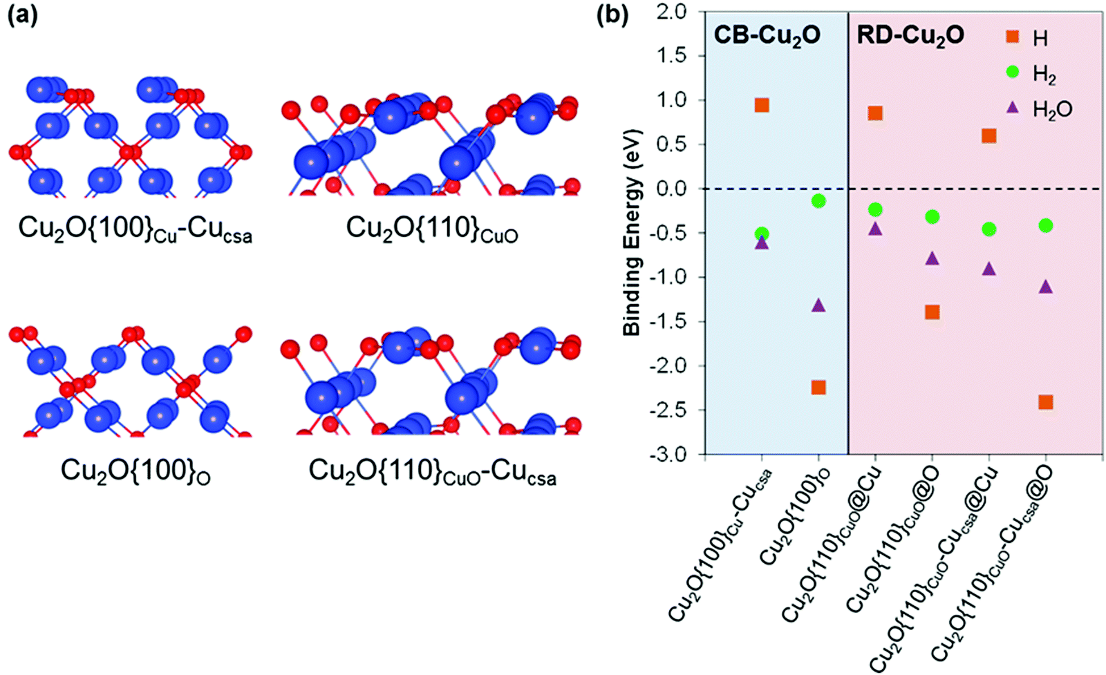 | ||
| Fig. 3 (a) Atomic arrangement of thermodynamically stable Cu2O {100} and {110} exposed facet with distinctive terminating surface, blue represents Cu atom and red represents O atom, and (b) modelled surface adsorption ability of H, H2 and H2O of Cu2O {100} and {110}. Cu2O{100}Cu-Cucsa: Cu-terminated Cu2O{100} with a coordinatively saturated Cu removed, Cu2O{100}o: O-terminated Cu2O{100}, Cu2O{110}CuO: CuO-terminated Cu2O{110} and Cu2O{110}CuO-Cucsa: CuO-terminated Cu2O{110} with coordinatively saturated Cu removed. The @O and @Cu denotes adsorption at O and Cu active sites, respectively. | ||
2.3. Surface electronic structure
In the case of surface electronic structure, variations in band structure have been demonstrated to influence the intrinsic carrier dynamics of a semiconductor. A first insight in the differences in surface electronic structure of CB-Cu2O and RD-Cu2O can be obtained by correlating the measured bandgap to their respective valence band positions determined from linear sweep voltammetry (LSV, to determine the on-set potential) and valence band XPS measurements.11 The onset potential for a p-type semiconductor is defined as the most positive potential at which the cathodic photocurrent still coincides with the dark current.43 These values (i.e. +0.59 and +0.69 V vs. RHE for CB-Cu2O and RD-Cu2O, as tabulated in Table S2, ESI†) are obtained from LSV measurements under chopped irradiation (Fig. S3a, ESI†) and can be used as a first-order approximation of their corresponding flat band potentials.44 In addition, valence band XPS (Fig. S3b, ESI†) was conducted to measure the potential difference between the valence band maxima and the Fermi levels.11 From extrapolation, the valence band of CB-Cu2O and RD-Cu2O are determined to lie at +0.94 and +1.00 V vs. RHE, respectively. Subsequently, the conduction band positions were calculated by adding the band gap energies to the valence band positions, resulting in values of −1.08 V for CB-Cu2O and −1.00 V for RD-Cu2O, both with respect to RHE. All these band position values are compiled to give schematic band structures as illustrated in Fig. 4a (also tabulated in Table S2, ESI†).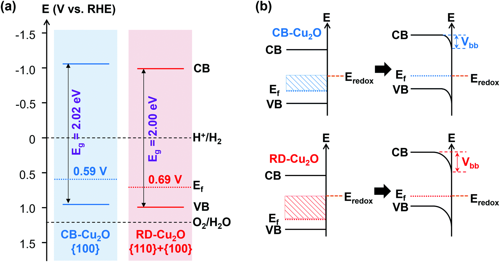 | ||
| Fig. 4 (a) Postulated electronic band structures and (b) expected downward band bending at the semiconductor/electrolyte junctions of CB-Cu2O and RD-Cu2O. | ||
Fig. 4a shows that the Fermi levels of both samples are closer to the valence band than to the conduction band, which again confirms the p-type nature of both Cu2O samples. The conduction and valence bands of the rhombic dodecahedral {110}-dominated sample (RD-Cu2O) are located at a more positive position when compared to the cubic {100}-faceted Cu2O (CB-Cu2O), in agreement with the literature.45 This surface potential shift is often deduced as one of the factors governing the carrier transfer efficiency and thus, enhancing the photoactivity. When the samples are in contact with an electrolyte, the semiconductor/electrolyte junctions were formed due to the difference in potentials between the semiconductors and the electrolyte. After the equilibration of these interfaces, a downward band bending (Vbb, for p-type semiconductor) is created, as demonstrated in Fig. 4b. This potential gradient enhances the carrier separation efficiency and thereby increases the fraction of photoexcited electrons that arrives at the surface. Since the Fermi level of RD-Cu2O is located at a more positive potential, the equilibration leads to a higher degree of band bending (Fig. 4b). Although the difference is relatively small, the larger band bending of RD-Cu2O is often a typical reason used to justify the better PC and PEC performance, owing to the improved charge transfer for photoreduction.46
2.4. Defect density
Apart from surface atomic structures and surface electronic structures, defect density is another property that may be tuned when synthesizing Cu2O with different exposed facets. To evaluate the defect density, XPS investigations were performed on CB-Cu2O and RD-Cu2O samples. The O 1s spectra (Fig. 5a) show the presence of three distinct oxygen species: lattice oxygen of Cu2O (Cu+OL), adsorbed oxygen (Oads) and oxygen from water vapor/moisture (OH2O) with their corresponding peaks at the binding energies of 530.6, 531.9 and 533.0 eV, respectively.47 Considering that Oads is associated with oxygen vacancies,48 the larger peak area of Oads shown by CB-Cu2O indicates that this sample contains more surface oxygen vacancies than RD-Cu2O. For Cu 2p3/2 spectra (Fig. 5b), in addition to the dominant peak at 932.8 eV that corresponds to Cu(I) oxidation state of Cu2O, two peaks at higher binding energies (934.4 and 935.8 eV) which are ascribed to Cu(II) oxidation state and Cu(OH)2 are also observed in both samples.49,50 Note that the copper species at 934.4 eV (Cu2+) is attributed to the presence of a copper defect rather than to CuO, given that only a single peak at 916.6 eV related to Cu2O was detected from the Cu LMM Auger spectra (Fig. 5c).51 The higher intensity of the Cu2+ peak for CB-Cu2O suggests that it contains a higher concentration of copper defects when compared to RD-Cu2O. This is further confirmed by electron paramagnetic resonance (EPR) spectroscopy. Since Cu2+ is a paramagnetic species, the presence of copper deficiencies can be detected using EPR. Indeed, an EPR signal at a g-value of 2.06 corresponding to Cu2+ was observed for both samples, as illustrated in Fig. 5d.52 The more intense EPR signals of CB-Cu2O demonstrate the existence of a higher amount of copper defects, consistent with the XPS data. Overall, the XPS and EPR results convincingly show that CB-Cu2O has more structural defects (i.e. oxygen vacancies and copper deficiencies) than RD-Cu2O. This indicates that apart from surface atomic structures and surface electronic structures, the nature and concentration of defects should be considered as one of the facet-dependent properties that should not be overlooked.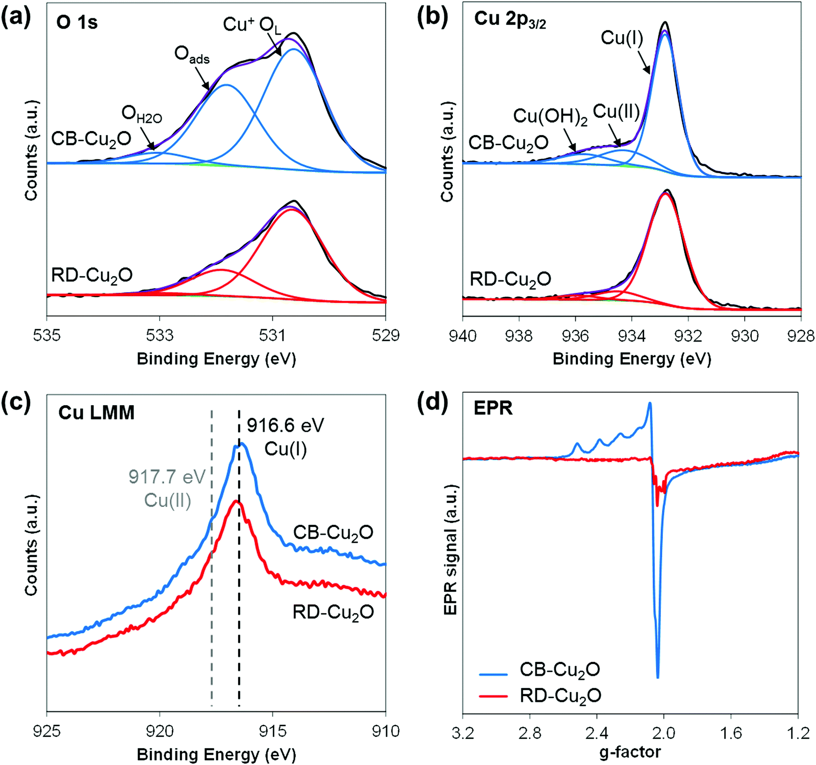 | ||
| Fig. 5 (a) O1s, (b) Cu2p3/2, (c) Cu LMM spectra from XPS measurement and (d) EPR spectra for CB-Cu2O and RD-Cu2O. | ||
2.5. Carrier dynamics
Both CB-Cu2O and RD-Cu2O exhibit distinct facet-dependent properties as mentioned above. Nonetheless, the dominant governing factors that dictate photocatalytic performance are often related to the intrinsic charge dynamics, which are also affected by changes in the above-mentioned facet-dependent properties (i.e. surface electronic structure and defect density). In order to gain insight into Cu2O carrier dynamics, time-resolved microwave conductivity (TRMC), photoluminescence (PL) and surface photovoltage spectroscopy (SPV) measurements were conducted on CB-Cu2O and RD-Cu2O.TRMC is a contactless technique for measuring the photoconductivity of a semiconductor. The data can then be used to determine the sum of the charge carrier mobilities (∑μ) and the effective lifetime (τeff) of the carriers. The TRMC system utilizes a nanosecond pulsed laser to excite the sample which generates mobile carriers (i.e. electrons and holes) that modify the reflected microwave power.53,54Fig. 6a shows the microwave conductance transients of CB-Cu2O and RD-Cu2O obtained after excitation with a 355 nm laser pulse of 7.0 × 10¹² photons pulse−1 cm−2. While CB-Cu2O achieves a maximum TRMC signal (i.e. ϕ∑μ, see Experimental section for definition) of 0.006 cm2 V−1 s−1, the signal for RD-Cu2O is larger by almost two orders of magnitude (0.19 cm2 V−1 s−1). TRMC measurements with varying laser pulse intensities also confirm that RD-Cu2O consistently exhibits much higher maximum ϕ∑μ values than CB-Cu2O, as portrayed in Fig. 6b. Note that the decrease of ϕ∑μ with increasing laser pulse intensity is attributed to higher-order non-geminate electron–hole recombination.55,56 The reduced recombination at lower light intensities thus contributes to the plateau (intensity-independent ϕ∑μ) that is observed, particularly for RB-Cu2O at the region of low laser pulse intensities. Since the maximum ϕ∑μ can be taken as a representative value of the effective carrier mobility in a semiconductor, the results suggest that RD-Cu2O has substantially higher carrier mobility when compared to that of CB-Cu2O. The remarkably higher carrier mobility of RD-Cu2O is also validated by the good signal-to-noise ratio generated with a laser pulse intensity as low as 2.0 × 10¹⁰ photons pulse−1 cm−2, while clear photoconductance signals for CB-Cu2O can only be obtained at higher laser pulse intensities (>1012 photons pulse−1 cm−2). Similar trends are observed for TRMC measurements at 532 nm laser pulse irradiation (Fig. S4, ESI†), which again confirms the excellent carrier mobility of RD-Cu2O in comparison to CB-Cu2O. This finding is also in accordance with the recently reported TRMC measurements of Cu2O, demonstrating a much higher charge mobility of polyhedral Cu2O when compared to cubic Cu2O.57
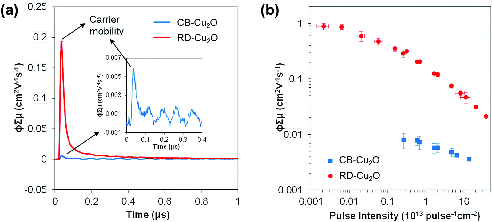 | ||
| Fig. 6 (a) TRMC signal of CB-Cu2O and RD-Cu2O over time at 7.0 × 10¹² photons pulse−1 cm−2, with the inset showing the magnification of the signal of CB-Cu2O, and (b) maximum TRMC signal as a function of incident pulse intensity of CB-Cu2O and RD-Cu2O. | ||
The effective carrier lifetimes of the two Cu2O samples were determined from the decay of their TRMC signals as shown in Fig. 6a. Each of the curves can be well-fitted to a bi-exponential decay, in which the derived decay time constants (τ1 and τ2) are tabulated in Table 1. Both the τ1 and τ2 for CB-Cu2O are smaller than that of RD-Cu2O, suggesting that the charge carriers recombine/trap faster in CB-Cu2O. This is attributed to the presence of more structural defects in this sample, as validated by the XPS and EPR analyses results above. Such structural defects are reported to be associated with the trapping of carriers, thereby acting as a deleterious charge recombination sites.38 Based on the obtained effective carrier mobility and lifetime (τeff), the effective carrier diffusion length (LD,eff) of CB-Cu2O and RD-Cu2O were estimated according to eqn (1) and (2).
 | (1) |
 | (2) |
| Samples | Carrier lifetime, τeff (ns) | Diffusion length, LD,eff (nm) | ||
|---|---|---|---|---|
| τ 1 | τ 2 | From τ1 | From τ2 | |
| CB-Cu2O | 14.3 ± 1.5 | 257.0 ± 8.8 | 14.7 ± 0.7 | 63.2 ± 11.4 |
| RD-Cu2O | 22.2 ± 4.0 | 281.0 ± 9.1 | 97.9 ± 10.3 | 280.9 ± 38.7 |
Apart from that, dark microwave conductivity measurements (refer to ESI† for detailed calculations) were also performed to determine the conductivity (σ) and carrier density (Na) of CB-Cu2O and RD-Cu2O.58 As tabulated in Table S3 (ESI†), CB-Cu2O has a higher carrier density and thus a higher conductivity than RD-Cu2O. This can be explained by the existence of a higher concentration of defects in CB-Cu2O, which typically contribute to electron trapping. This increases the Na and accordingly the σ, based on eqn (3).
| σ = eNaμ | (3) |
 | (4) |
The extent of electron–hole pair recombination in CB-Cu2O and RD-Cu2O was also studied with steady-state photoluminescence (PL) spectroscopy. Although an emission band at 615 nm, which corresponds to band-to-band recombination, are exhibited by both types of Cu2O, the PL intensity of CB-Cu2O is noticeably higher than that of RD-Cu2O (Fig. S5, ESI†). This implies that the rate of band-to-band recombination is higher than that of RD-Cu2O. This therefore indicates that the higher defect concentration leads to poor charge separation of CB-Cu2O, which is detrimental to the overall performance, in accordance with its shorter effective carrier lifetime deduced from the TRMC decay curve. Collectively, despite having higher carrier density, the photoactivity in PC and PEC systems of conductive CB-Cu2O is hindered by its significantly lower carrier mobility and shorter carrier lifetime.
In addition to TRMC and PL spectroscopy, modulated surface photovoltage (SPV) spectroscopy measurements were performed to distinguish the dominating mechanism of charge separation and relaxation in CB-Cu2O and RD-Cu2O. In contrast to our expectation, the SPV signals for the RD-Cu2O sample (larger band bending) are not larger than those of the CB-Cu2O sample; instead, CB-Cu2O showed up to 2 orders of magnitude higher SPV signals than RD-Cu2O (Fig. 7a, b and Fig. S6, ESI†) at different modulation frequencies. This observation is unlikely to be the result of the surface band bending difference as discussed above. Alternatively, the SPV spectra provide further information of the presence of surface trap states (i.e. defects, as confirmed by XPS and EPR) that are shown to be detectable by SPV spectroscopy,60,61 and dominating mechanisms of charge separation in CB-Cu2O and RD-Cu2O (as explained below). As previously reported, a higher copper deficiency (Cu2+) results in stronger negative in-phase SPV signals,32 which is in accordance to the intense SPV signals of CB-Cu2O that possesses higher defect density when compared to RD-Cu2O.
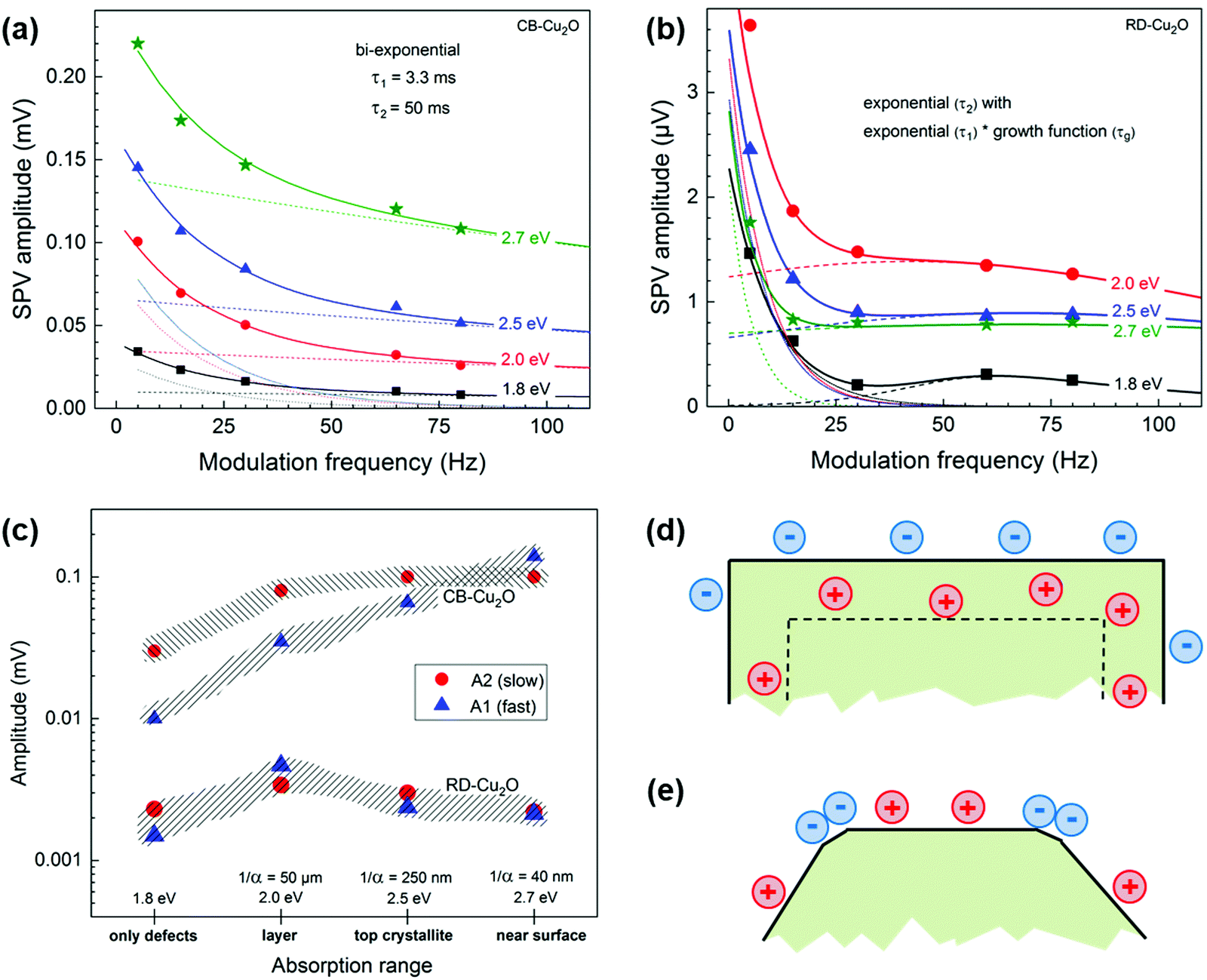 | ||
| Fig. 7 Dependencies of the SPV amplitude on modulation frequency measured at photon energies of 1.8, 2.0, 2.5 and 2.7 eV (squares, circles, triangles and stars, respectively) of (a) CB-Cu2O (solid line is the bi-exponential fits, while dotted and dashed lines show the two separate exponentials, respectively) and (b) RD-Cu2O (the solid line shows an exponential fits with a peak indicating the product of an exponential with a logistic growth function, while the thin dotted and dashed lines show the corresponding separate exponentials and peaks, respectively). (c) Summary of the dependencies of the amplitudes of the “fast” (triangles) and “slow” (circles) processes on the (qualitative) absorption range for CB-Cu2O (upper part) and RD-Cu2O (lower part). Schematic distribution of positive surface charge and negative charge (d) in a surface space charge region (depletion layer) within a doped homogeneous CB-Cu2O and (e) modulated by different facets of RD-Cu2O. | ||
Fig. S6 (ESI†) shows the modulated SPV spectra of in-phase and 90° phase-shifted signals of CB-Cu2O and RD-Cu2O measured at 5, 15 and 80 Hz. The negative in-phase signal indicates that photogenerated electrons are separated preferentially towards the external surface, similar to the phenomenon observed by Chen et al.5 For CB-Cu2O (Fig. S6a, ESI†), the SPV signals start to appear at approx. 1 eV and further intensified at 2 eV (band gap of Cu2O). The emergence of the signal at lower photon energies (<2 eV) is due to the presence of defects in CB-Cu2O, consistent with our XPS and EPR results. The dependencies of the SPV amplitudes on the modulation frequency are depicted in Fig. 7(a) and (b) for photon energies of 1.8, 2.0, 2.5 and 2.7 eV (i.e. in the ranges below the band gap, near the band gap, in the local minimum and near the second maximum, respectively, refer to ESI† for detailed explanation). In contrast to CB-Cu2O, the highest SPV amplitudes are reached for RD-Cu2O at a photon energy of 2.0 eV and the SPV amplitudes do not decrease monotonously with increasing frequency, as illustrated in Fig. 7b. In order to understand the dominating mechanisms of charge separation in CB-Cu2O and RD-Cu2O, the dependencies of the amplitudes for the “fast” (A1) and “slow” (A2) processes are calculated by fitting Fig. 7a and b to their corresponding functions described by eqn (S4) and (S5) (ESI†), respectively. A1 and A2 are compared as a function of the (qualitative) absorption range. Photons with energies at 1.8 eV represent the absorption by transitions from defect states into the conduction or valence bands of Cu2O, while the absorption lengths (1/α) at the photon energies of 2.0, 2.5 and 2.7 eV are approximately 50 μm, 250 nm and 40 nm, respectively.59 By comparing the absorption lengths to the CB-Cu2O and RD-Cu2O particle size (i.e. approx. 500 nm), the absorption ranges for excitation at 1.8, 2.0, 2.5 and 2.7 eV therefore, corresponding to homogeneous absorption by defects, homogeneous absorption through the whole particle, absorption only in the Cu2O crystallites closest to the reference electrode (top crystallites) and absorption within a very thin near surface layer, respectively.
Fig. 7c summarizes the dependencies of A1 and A2 as a function of the absorption range for CB-Cu2O and RD-Cu2O. For CB-Cu2O, A1 increases from 10 μV (1.8 eV) to 140 μV (2.7 eV), while A2 initially increases from 30 μV (1.8 eV) to 80 μV at 2.0 eV and saturation at 100 μV at higher photon energies. Given that the amplitude of the “fast” process (A1) increases continuously with decreasing absorption length, while the amplitude of the “slow” process (A2) saturates at higher photon energies, the “fast” processes are likely related to the absorption within a thin near-surface layer while the “slow” processes correspond to the absorption over the whole Cu2O particles. For RD-Cu2O, A1 and A2 increase from 1.5 and 2.3 μV (1.8 eV), to 4.5 and 3.5 μV (2.0 eV), then decreases to 2.5 and 3.0 μV (2.5 eV) and finally to 2.0 and 2.2 μV (2.7 eV). The variations are considered insignificant, given the facts that, first, the modulated SPV signals of RD-Cu2O are very low and, second, the signals even decrease with decreasing absorption length, despite the improved photocatalytic performance. Interestingly, the constant τ1 and τ2 used to fit the SPV amplitudes of CB-Cu2O across various frequencies (refer to ESI† for more details) has shown that τ1 and τ2 are independent of the photon energies and absorption lengths, signifying homogeneous charge separation within CB-Cu2O. On the other hand, the time constants for RD-Cu2O (particularly, the “fast” time constant) decrease with increasing photon energies, demonstrating that charge separation is not homogeneous in RD-Cu2O.
Modulated SPV signals correspond to the charge separation length projected to the normal reference electrode. In CB-Cu2O, the “fast” and “slow” processes are independent of the absorption range, indicating that there is one common driving force of charge separation. This common driving force is related to the built-in electrical field perpendicular to the surfaces of the facets. Given that CB-Cu2O is a p-type doped semiconductor with moderate densities of equilibrium charge carriers, the width of the surface space charge region is of the order of 100 nm, which is significantly shorter than the half extension of one CB-Cu2O particle. Therefore, a homogeneously distributed opposite built-in electrical field perpendicular to the facets of CB-Cu2O is the driving force for charge separation, facilitating separation of majority charge carrier (holes) inwards, as illustrated in Fig. 7d. In RD-Cu2O, the phenomenon is completely different than that in CB-Cu2O since built-in electrical fields can be neglected, due to the lower density of equilibrium charge carriers (aligned with our dark microwave conductivity measurement results).59 The enhanced photocatalytic activity in RD-Cu2O is attributed to the effective driving force for local charge separation, such as charge separation towards different directions. Although RD-Cu2O is dominantly enclosed by {110} facets, the facet corners are not sharp and small facets (i.e. {100} facets) can be observed. The existence of secondary facets within RD-Cu2O presents an additional driving force for the charge to be separated effectively towards different exposed facets (photogenerated electrons to {100} and holes to {110}), as delineated by Li et al.62 Selective photodeposition of Ag (Fig. S7, ESI†) was performed to further confirm the spatial separation of charges within RD-Cu2O. Ag nanoparticles were randomly deposited on CB-Cu2O (Fig. S7a, ESI†) and selectively deposited on the corners of RD-Cu2O, as illustrated in Fig. S7b (ESI†). This signifies that the photogenerated electrons preferentially migrated to the corners of RD-Cu2O (i.e. {100} facets), in accordance with the SPV results. As a result, the modulated charge separation across the surface of RD-Cu2O is another reason for its enhanced photocatalytic performances.
In short, TRMC shows the significant improvement of effective carrier mobility and lifetime of RD-Cu2O, while PL and SPV also demonstrate its enhanced local charge separation efficiency. These results have consistently shown the carrier dynamics of RD-Cu2O to be superior, which is the reason behind the enhanced photoactivity in PC and PEC systems. Note that, one may be tempted to conclude that the differences in the surface atomic and electronic structure (the typical facet-dependent properties) are the dominant factors affecting the overall performance, since several studies showed that differences in the surface electronic structure and band bending greatly affect the performance of the photocatalyst.27–29,59 However, the collative results from this study clearly show that the structural defect densities and existence or secondary facet/facet boundaries also play vital roles in determining the carrier dynamic of a semiconductor, and the photoreactivity of a photocatalyst is highly dependent on its intrinsic charge dynamics. In addition, the higher trapping density in CB-Cu2O (due to the higher defect concentration) that enhances its conductivity and intensifies the SPV signals does not assure its good photocatalytic ability due to its inferior charge mobility and carrier separation efficiency. CB-Cu2O with a homogeneous depletion layer at the surface prompts the photo-generated majority charge carriers (holes) to separate towards the center of the crystallite. Those charge carriers induce an electric field in the opposite direction, which increases the recombination rate during photocatalysis, supported by our PL results. In contrast, RD-Cu2O with modulated charges in surface states enables photogenerated minority and majority charge carriers to separate towards different regions on the surface, where these photogenerated charges could participate in photocatalytic reactions.
3. Conclusion
Carrier dynamics within a faceted semiconductor are demonstrated to govern the photoactivity of PC H2 generation and PEC photocurrent measurement. In this study, RD-Cu2O (i.e. dominant {110} exposed facets) is shown to have better performances when compared to CB-Cu2O with all {100} exposed facets, attributed to the higher carrier mobility determined from the contactless TRMC measurement and better charge separation efficiency demonstrated by PL and SPV measurements. Although the surface atomic arrangement and the surface electronic band structure are commonly identified as the main factors that boost the photocatalytic performance of faceted Cu2O, the inevitable evolution of defects during the synthesis and the presence of secondary facets are shown to affect the carrier dynamics of the samples. The higher defect concentrations formed within CB-Cu2O increases its conductivity and carrier density. However, our results show that the higher defect density presents a detrimental effect on carrier mobility and separation, thus hinders the photoactivity of CB-Cu2O. On the other hand, the superior carrier mobility, lifetime and diffusion length of the RD-Cu2O sample are the dominant factors that enhance the performance in PC and PEC systems. Moreover, despite the stronger SPV signals of CB-Cu2O, the homogeneous depletion layer induces an opposite electric field on CB-Cu2O and increases the charge recombination rate, while RD-Cu2O with the presence of secondary facets allows efficiency charge separation towards different directions of the surfaces. In this work, all the possible facet-dependent properties involved in crystal facet engineering were carefully interpreted. Apart from surface absorption abilities and surface energies, these findings demonstrate that surface defect density (formed during the fabrication of faceted Cu2O) and exposure of more than one facets are important factors that influence the photoactivity and should not be neglected.4. Experimental section
Material preparation
A facile solution-phase method adapted from Liang et al.1 was used to fabricate cuprous oxide in this work. Initially, 80 mL of 0.05 M CuSO4·5H2O (>99%, UNIVAR) was mixed with 40 mL of ethanol (100% unsaturated, chem-supply) followed by heating to 80 °C under constant stirring. 20 mL of 0.8 M aqueous sodium hydroxide (NaOH, >98%, chem-supply) solution was then added and the suspension was held for another 5 min before the addition of 60 mL D-glucose (6.42 g, anhydrous, chem-supply) solution. Cubic Cu2O powder was then washed alternately with Milli-Q water and ethanol before drying in a vacuum desiccator. For rhombic dodecahedral Cu2O, the procedure was repeated with the addition of 12 mL oleic acid (analytical standard, Sigma Aldrich) and the suspension was maintained at a temperature of 100 °C.Material characterizations
The morphologies and structures of the samples were examined by field-emission scanning electron microscopy (FE-SEM, FEI Nova NanoSEM 450). Crystallinity was investigated using X-ray diffraction (XRD, X'pert MPD with Cu Kα radiation at 45 kV and 40 mA). UV-Vis absorbance spectra were converted from diffuse reflectance spectra obtained on a Shimadzu UV 3600 spectrophotometer with BaSO4 as reference using the Kubelka–Munk transformation. The Brunauer–Emmett–Teller (BET) surface area of Cu2O was assessed using a Micromeritics Tristar 3030 Analyser at 77 K. Before the measurement, the samples were pre-treated at 150 °C for three hours in a Micrometric VacPrep unit.The surface composition and valence band spectra of the samples were analysed via X-ray photoelectron spectroscopy (XPS, Thermo ESCALAB250Xi) probed with monochromatic Al Kα radiation (hv = 1486.68 eV) in a vacuum chamber. The C 1s peak at 284.4 eV was used to calibrate the binding energy before spectra deconvolution. Electron paramagnetic resonance (EPR) measurements were carried out on Bruker EMX-plus operating at a 9.41 GHz frequency (X-band) with a microwave power of 2 mW at a temperature of 125 K. Photoluminescence spectra were obtained using Horiba Fluoromax-4 spectrofluorometer with an excitation wavelength of 525 nm.
Photocatalytic hydrogen (H2) generation
Photocatalytic H2 evolution was performed with top illumination through the quartz window of an enclosed Y-reactor. 50 mg of samples were dispersed in 200 mL of 0.5 M Na2SO3 solution. Prior to illumination, argon gas (100%, Coregas) was used to deaerate the suspension for 30 min to remove all the dissolved gases. A 300 W xenon lamp (CERMAX) with an intensity of 385 mW cm−2 was employed as the light source (Light spectrum provided in Fig. S8, ESI†). H2 evolved during the illumination was monitored by a gas chromatograph (Shimadzu GC-8A, HayeSep DB column) at 30 min intervals. After the reaction, the post-reaction catalyst was retrieved by centrifugation (10![[thin space (1/6-em)]](https://www.rsc.org/images/entities/char_2009.gif) 000 rpm for 15 min) for further characterizations. The solid sample collected was further dispersed in MilliQ water and centrifuged (repeated for three times) to remove any salt (Na2SO3 or Na2SO4, oxidized from Na2SO3) residue deposited on the surface of the catalyst during the reaction. Finally, the solid catalyst was dried and kept in a vacuum desiccator before characterizations. Control experiments were performed using the same enclosed Y-reactor containing 50 mg of photocatalyst dispersed in 200 mL of 0.5 M Na2SO3 solution without light irradiation.
000 rpm for 15 min) for further characterizations. The solid sample collected was further dispersed in MilliQ water and centrifuged (repeated for three times) to remove any salt (Na2SO3 or Na2SO4, oxidized from Na2SO3) residue deposited on the surface of the catalyst during the reaction. Finally, the solid catalyst was dried and kept in a vacuum desiccator before characterizations. Control experiments were performed using the same enclosed Y-reactor containing 50 mg of photocatalyst dispersed in 200 mL of 0.5 M Na2SO3 solution without light irradiation.
Photoelectrochemical (PEC) measurement
Drop casted samples on FTO substrates (2 mg cm−2) were used for PEC measurements. To obtain a 2 mg cm−2 Cu2O thin film, bare FTO was cleaned thoroughly in ethanol, acetone and milliQ water. Next, 6 mg of Cu2O were dispersed in 6 mL of ethanol via sonication for at least 15 min. 0.1 mL of the suspension containing Cu2O was then dropped on a 3 cm2 cleaned FTO at room temperature. This step was repeated at a 15 min interval until all the suspension was dropcasted. During the dropcasting process, it is crucial to ensure that the film is completely dried before the subsequent layer was deposited to avoid segregation of particles and create an evenly distributed Cu2O thin film. A three-electrode PEC system with a Cu2O working electrode, Ag/AgCl reference electrode, Pt counter electrode immersed in 0.1 M Na2SO4 solution was employed to evaluate the PEC responses. Photocurrent densities were recorded as amperometry curves and on-set potentials were determined from linear sweep voltammetry curves using a potentiostat (Model PGSTAT302N, Autolab) under on–off irradiation by 300 W xenon lamp (CERMAX).Density functional theory (DFT) calculations
Electronic structure calculations were performed using DFT as implemented in VASP.63,64 Core and valence electronics were described using the projector augmented wave (PAW) method and exchange–correlation parametrization according to the PBE functional.65 The wavefunctions were expanded in the planewave basis using an energy cutoff of 500 eV. Dispersion effects were corrected for using Grimme van der Waals parameters.66 Surfaces were constructed using symmetric slabs with 15–17 atomic layers separated by ∼20 Å of vacuum to reduce interaction along the periodic z-direction. To correctly account for electronic correlations, a GGA+Ueff (Ueff = 7 eV) was used. A Ueff value in the range of 5–8 eV was shown to reproduce key electronic and geometric properties of Cu2O.67–69 All atomic positions were allowed to relax until forces were less than 0.01 Å eV−1 and self-consistent field energies change by no more than 1 × 10⁻⁵ eV. The adsorbate binding energies are calculated using eqn (5),| Eb(H*) = Etot(H*) − Etot(surface) − 1/2Etot(H2) | (5) |
Time resolved microwave conductivity (TRMC) measurement
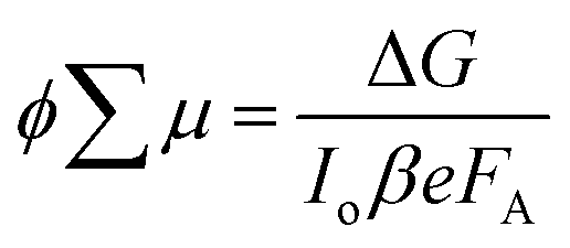
For TRMC measurements, the films were prepared by drop casting the samples (2 mg cm−2) on a 25 mm × 12 mm quartz substrate at room temperature. The substrate was then mounted to a specially designed microwave cavity cell, and the cell was fitted into a setup consisting of a microwave source (X-band, 8.4–8.7 GHz), a Q-switched Nd:YAG laser (λ = 355 or 532 nm, i.e. frequency-tripled or -doubled) and a microwave detector as illustrated in other works.56,70 The resonant frequency of the cavity loaded with our Cu2O samples was found to be 8.51 GHz; this frequency was employed in all our measurement. The changes in reflected microwave power from the cavity upon 6.0 ns FWHM pulsed laser excitation, ΔP/P, were monitored throughout the measurement. This value was then used to calculate the change in the conductance of the sample, ΔG according to eqn (6). The correlations between the measured changes in microwave power (ΔP/P), conductance (ΔG) and carrier mobility (μ) allow the TRMC signal to be expressed as a product of internal quantum efficiency (ϕ) and the sum of carrier mobility (∑μ). Using this ΔG value, the product of the internal quantum efficiency (ϕ, which is the number of excited mobile carriers normalized to the number of absorbed photons, typically taken as 1 for an inorganic semiconductor) and the sum of carrier mobility (∑μ) can be computed following eqn (7). Here, for both wavelengths (355 and 532 nm), pulsed laser intensities were adjusted using a neutral density filter, and the values were between 1010 and 1015 photons cm−2 pulse−1. | (6) |
 | (7) |
Modulated surface photovoltage (SPV) spectroscopy measurement
Modulated SPV spectroscopy measurements were performed in a fixed capacitor arrangement, as reported previously.72 The SPV signals were measured using high-impedance buffers (input impedance of 150 GΩ). A halogen lamp with a quartz prism monochromator (SPM2, Zeiss) was used for modulated illumination. A mechanical chopper was placed in front of the entrance slit of the monochromators. The modulated in-phase and quadrature (i.e. 90° out-of-phase) signals were detected with a dual-phase DSP lock-in amplifier (EG&G 7260). The phase was calibrated with a Si photodiode. In modulated SPV spectroscopy, signals are measured in accordance to the phase of the modulation. The in-phase signals follow the modulation and give information about the “fast” response in relation to the modulation period. In contrast, signals phase-shifted by 90° give information about the “slow” response. The SPV amplitude (R) is defined as the square root of the sum of the squared in-phase and phase-shifted by 90° signals (refer to reported literature).34 Modulated SPV spectra were measured at different modulation frequency (fmod) in order to distinguish dominating mechanisms of charge separation and relaxation.Photodeposition of Ag nanoparticles
Photodeposition of Ag on CB-Cu2O and RD-Cu2O were performed in the same reactor system as photocatalytic H2 generation (top illumination through quartz window of an enclosed Y-reactor). 50 mg of samples were dispersed in 200 mL of 0.25 mM aqueous AgNO3 solution. The system was purged with Ar gas for at least 30 min to remove O2 that could potentially compete with Ag deposition reaction. The suspension was illuminated for an hour before retrieving the products (Ag-deposited Cu2O particles) via centrifugation.Conflicts of interest
There are no conflicts to declare.Acknowledgements
This work was financially supported by the Australian Research Council Discovery Project (DP180102540) and Hong Kong General Research Fund (GRF11305419 and GRF11306920). The authors appreciate the facility and technical support provided by the UNSW Mark Wainwright Analytical Centre. The authors acknowledge Dr Dennis Friedrich for his inputs during time-resolved microwave conductivity measurements in Helmholtz-Zentrum Berlin.References
- E. S. Jang, J. H. Won, S. J. Hwang and J. H. Choy, Adv. Mater., 2006, 18, 3309–3312 CrossRef CAS.
- R. Li, F. Zhang, D. Wang, J. Yang, M. Li, J. Zhu, X. Zhou, H. Han and C. Li, Nat. Commun., 2013, 4, 1432 CrossRef PubMed.
- C. Zhang and Y. Zhu, Chem. Mater., 2005, 17, 3537–3545 CrossRef CAS.
- J. Pan, G. Liu, G. Q. M. Lu and H. M. Cheng, Angew. Chem., Int. Ed., 2011, 50, 2133–2137 CrossRef CAS PubMed.
- X. Liang, L. Gao, S. Yang and J. Sun, Adv. Mater., 2009, 21, 2068–2071 CrossRef CAS.
- X. Peng, L. Manna, W. Yang, J. Wickham, E. Scher, A. Kadavanich and A. P. Alivisatos, Nature, 2000, 404, 59–61 CrossRef CAS PubMed.
- Y. Sun and Y. Xia, Science, 2002, 298, 2176–2179 CrossRef CAS PubMed.
- T. Ohno, K. Sarukawa and M. Matsumura, New J. Chem., 2002, 26, 1167–1170 RSC.
- H. L. Tan, X. Wen, R. Amal and Y. H. Ng, J. Phys. Chem. Lett., 2016, 7, 1400–1405 CrossRef CAS PubMed.
- L. Zhang, W. Wang, S. Sun, D. Jiang and E. Gao, Appl. Catal., B, 2015, 162, 470–474 CrossRef CAS.
- X. Wu, Y. H. Ng, L. Wang, Y. Du, S. X. Dou, R. Amal and J. Scott, J. Mater. Chem. A, 2017, 5, 8117–8124 RSC.
- H. Wu, Z. Zheng, C. Y. Toe, X. Wen, J. N. Hart, R. Amal and Y. H. Ng, J. Mater. Chem. A, 2020, 8, 5638–5646 RSC.
- L. Chen, Y. Zhang, P. Zhu, F. Zhou, W. Zeng, D. D. Lu, R. Sun and C. Wong, Sci. Rep., 2015, 5, 9672 CrossRef PubMed.
- C. H. B. Ng and W. Y. Fan, J. Phys. Chem. B, 2006, 110, 20801–20807 CrossRef CAS PubMed.
- J. Xu and D. Xue, Acta Mater., 2007, 55, 2397–2406 CrossRef CAS.
- L. Gou and C. J. Murphy, Nano Lett., 2003, 3, 231–234 CrossRef CAS.
- Y. Zhao, W. Wang, Y. Li, Y. Zhang, Z. Yan and Z. Huo, Nanoscale, 2014, 6, 195–198 RSC.
- C.-H. Kuo and M. H. Huang, J. Am. Chem. Soc., 2008, 130, 12815–12820 CrossRef CAS PubMed.
- X. Lu, J. N. Hart, Y. Yao, C. Y. Toe, J. Scott and Y. H. Ng, Mater. Today Energy, 2020, 16, 100422 CrossRef.
- Y. Zhang, B. Deng, T. Zhang, D. Gao and A.-W. Xu, J. Phys. Chem. C, 2010, 114, 5073–5079 CrossRef CAS.
- C. Y. Toe, Z. Zheng, H. Wu, J. Scott, R. Amal and Y. H. Ng, J. Phys. Chem. C, 2018, 122, 14072–14081 CrossRef CAS.
- H. Bao, W. Zhang, D. Shang, Q. Hua, Y. Ma, Z. Jiang, J. Yang and W. Huang, J. Phys. Chem. C, 2010, 114, 6676–6680 CrossRef CAS.
- D.-F. Zhang, H. Zhang, L. Guo, K. Zheng, X.-D. Han and Z. Zhang, J. Mater. Chem., 2009, 19, 5220–5225 RSC.
- C. Y. Toe, J. Scott, R. Amal and Y. H. Ng, J. Photochem. Photobiol., C, 2019, 40, 191–211 CrossRef CAS.
- W.-C. Huang, L.-M. Lyu, Y.-C. Yang and M. H. Huang, J. Am. Chem. Soc., 2012, 134, 1261–1267 CrossRef CAS PubMed.
- Y. Kwon, A. Soon, H. Han and H. Lee, J. Mater. Chem. A, 2015, 3, 156–162 RSC.
- G. Z. Yuan, C. F. Hsia, Z. W. Lin, C. Chiang, Y. W. Chiang and M. H. Huang, Chem. – Eur. J., 2016, 22, 12548–12556 CrossRef CAS PubMed.
- Z. Zheng, B. Huang, Z. Wang, M. Guo, X. Qin, X. Zhang, P. Wang and Y. Dai, J. Phys. Chem. C, 2009, 113, 14448–14453 CrossRef CAS.
- C.-Y. Chu and M. H. Huang, J. Mater. Chem. A, 2017, 5, 15116–15123 RSC.
- S. Nishioka, J. Hyodo, J. J. M. Vequizo, S. Yamashita, H. Kumagai, K. Kimoto, A. Yamakata, Y. Yamazaki and K. Maeda, ACS Catal., 2018, 8, 7190–7200 CrossRef CAS.
- J. Zhu, S. Pang, T. Dittrich, Y. Gao, W. Nie, J. Cui, R. Chen, H. An, F. Fan and C. Li, Nano Lett., 2017, 17, 6735–6741 CrossRef CAS PubMed.
- R. Chen, S. Pang, H. An, T. Dittrich, F. Fan and C. Li, Nano Lett., 2019, 19, 426–432 CrossRef CAS PubMed.
- H. L. Tan, F. F. Abdi and Y. H. Ng, Chem. Soc. Rev., 2019, 48, 1255–1271 RSC.
- D. Thomas and F. Steffen, Surface photovoltage analysis of photoactive materials, World Scientific, 2020 Search PubMed.
- W. Ching, Y.-N. Xu and K. Wong, Phys. Rev. B, 1989, 40, 7684–7695 CrossRef CAS PubMed.
- H. Wu, H. L. Tan, C. Y. Toe, J. Scott, L. Wang, R. Amal and Y. H. Ng, Adv. Mater., 2020, 32, 1904717 CrossRef CAS PubMed.
- X. Wu, C. Y. Toe, C. Su, Y. H. Ng, R. Amal and J. Scott, J. Mater. Chem. A, 2020, 8, 15302–15318 RSC.
- A. Kudo and Y. Miseki, Chem. Soc. Rev., 2009, 38, 253–278 RSC.
- H. L. Tan, R. Amal and Y. H. Ng, J. Mater. Chem. A, 2017, 5, 16498–16521 RSC.
- G. Liu, C. Y. Jimmy, G. Q. M. Lu and H.-M. Cheng, Chem. Commun., 2011, 47, 6763–6783 RSC.
- C. Y. Toe, Z. Zheng, H. Wu, J. Scott, R. Amal and Y. H. Ng, Angew. Chem., Int. Ed., 2018, 57, 13613–13617 CrossRef CAS PubMed.
- A. Soon, M. Todorova, B. Delley and C. Stampfl, Phys. Rev. B, 2007, 75, 125420 CrossRef.
- A. Hagfeldt, S.-E. Lindquist and M. Grätzel, Sol. Energy Mater. Sol. Cells, 1994, 32, 245–257 CrossRef CAS.
- D. Scaife, Sol. Energy, 1980, 25, 41–54 CrossRef CAS.
- S. Lee, C.-W. Liang and L. W. Martin, ACS Nano, 2011, 5, 3736–3743 CrossRef CAS PubMed.
- Z. Zhang and J. T. Yates Jr, Chem. Rev., 2012, 112, 5520–5551 CrossRef CAS PubMed.
- W. Z. Wang, G. Wang, X. S. Wang, Y. Zhan, Y. Liu and C. L. Zheng, Adv. Mater., 2002, 14, 67–69 CrossRef CAS.
- H. L. Tan, A. Suyanto, A. T. D. Denko, W. H. Saputera, R. Amal, F. E. Osterloh and Y. H. Ng, Part. Part. Syst. Charact., 2017, 34, 1600290 CrossRef.
- S. Chawla, N. Sankarraman and J. Payer, J. Electron Spectrosc. Relat. Phenom., 1992, 61, 1–18 CrossRef CAS.
- M. Swadźba-Kwaśny, L. Chancelier, S. Ng, H. G. Manyar, C. Hardacre and P. Nockemann, Dalton Trans., 2012, 41, 219–227 RSC.
- D. Tahir and S. Tougaard, J. Phys.: Condens. Matter, 2012, 24, 175002 CrossRef PubMed.
- M. Łabanowska, E. Bidzińska, K. Dyrek, T. Fortuna, S. Pietrzyk, J. Rożnowski and R. P. Socha, Starch - Stärke, 2008, 60, 134–145 CrossRef.
- F. F. Abdi, T. J. Savenije, M. M. May, B. Dam and R. van de Krol, J. Phys. Chem. Lett., 2013, 4, 2752–2757 CrossRef CAS.
- M. de Respinis, M. Fravventura, F. F. Abdi, H. Schreuders, T. J. Savenije, W. A. Smith, B. Dam and R. van de Krol, Chem. Mater., 2015, 27, 7091–7099 CrossRef CAS.
- T. J. Savenije, A. Huijser, M. J. Vermeulen and R. Katoh, Chem. Phys. Lett., 2008, 461, 93–96 CrossRef CAS.
- J. E. Kroeze, T. J. Savenije and J. M. Warman, J. Am. Chem. Soc., 2004, 126, 7608–7618 CrossRef CAS PubMed.
- F. Plascencia-Hernández, A. L. Luna, C. Colbeau-Justin, P. Santiago, M. Garcia-Rocha, G. Valverde-Aguilar and M. A. Valenzuela, J. Saudi Chem. Soc., 2019, 23, 1016–1023 CrossRef.
- J. W. Jang, D. Friedrich, S. Müller, M. Lamers, H. Hempel, S. Lardhi, Z. Cao, M. Harb, L. Cavallo and R. Heller, Adv. Energy Mater., 2017, 7, 1701536 CrossRef.
- C.-S. Tan, S.-C. Hsu, W.-H. Ke, L.-J. Chen and M. H. Huang, Nano Lett., 2015, 15, 2155–2160 CrossRef CAS PubMed.
- J. Liqiang, Q. Yichun, W. Baiqi, L. Shudan, J. Baojiang, Y. Libin, F. Wei, F. Honggang and S. Jiazhong, Sol. Energy Mater. Sol. Cells, 2006, 90, 1773–1787 CrossRef.
- L. Kronik and Y. Shapira, Surf. Interface Anal., 2001, 31, 954–965 CrossRef CAS.
- R. Li, X. Tao, R. Chen, F. Fan and C. Li, Chem. – Eur. J., 2015, 21, 14337–14341 CrossRef CAS PubMed.
- G. Kresse and J. Furthmüller, Phys. Rev. B, 1996, 54, 11169 CrossRef CAS PubMed.
- G. Kresse and J. Furthmüller, Comput. Mater. Sci., 1996, 6, 15–50 CrossRef CAS.
- P. E. Blöchl, Phys. Rev. B, 1994, 50, 17953 CrossRef PubMed.
- S. Grimme, J. Comput. Chem., 2006, 27, 1787–1799 CrossRef CAS PubMed.
- M. Nolan and S. D. Elliott, Phys. Chem. Chem. Phys., 2006, 8, 5350–5358 RSC.
- L. I. Bendavid and E. A. Carter, J. Phys. Chem. C, 2013, 117, 26048–26059 CrossRef CAS.
- A. Živković, A. Roldan and N. H. De Leeuw, Phys. Rev. B, 2019, 99, 035154 CrossRef.
- J. T. Carneiro, T. J. Savenije and G. Mul, Phys. Chem. Chem. Phys., 2009, 11, 2708–2714 RSC.
- F. Weichman, Can. J. Phys., 1973, 51, 680–685 CrossRef CAS.
- V. Duzhko, V. Y. Timoshenko, F. Koch and T. Dittrich, Phys. Rev. B, 2001, 64, 075204 CrossRef.
Footnote |
| † Electronic supplementary information (ESI) available. See DOI: 10.1039/d1ma00934f |
| This journal is © The Royal Society of Chemistry 2022 |