
 Open Access Article
 This Open Access Article is licensed under a Creative Commons Attribution-Non Commercial 3.0 Unported Licence
Thermoelectric transport effects beyond single parabolic band and acoustic phonon scattering
Heng
Wang
 *a,
Ramya
Gurunathan
b,
Chenguang
Fu
c,
Runzi
Cui
a,
Tiejun
Zhu
c and
G. Jeffrey
Snyder
b
*a,
Ramya
Gurunathan
b,
Chenguang
Fu
c,
Runzi
Cui
a,
Tiejun
Zhu
c and
G. Jeffrey
Snyder
b
aDepartment of Mechanical, Materials and Aerospace Engineering, Illinois Institute of Technology, Chicago, IL 60616, USA. E-mail: heng.wang@iit.edu
bDepartment of Materials Science and Engineering, Northwestern University, Evanston, IL 60208, USA
cState Key Laboratory of Silicon Materials and School of Materials Science and Engineering, Zhejiang University, Hangzhou 310027, China
First published on 16th November 2021
Abstract
Thermoelectric materials have been extensively studied for applications in solid-state power generation and cooling. Progress has been made over the past decade in multiple materials systems, hence, it becomes increasingly valuable to be able to analytically model the transport behavior to optimize materials and compare different systems. The well-known effective mass modeling approach is often used to fit the data to the form expected for a single, parabolic band, with charge carrier scattering dominated by acoustic phonons, i.e., deformation potential scattering. However, many high-performance thermoelectric materials benefit from having multiple bands (multi-valley) and many have non-parabolic bands or complex scattering. Understanding how these effects alter properties from that given by the effective mass model provides rational strategies for new materials. In this review, we discuss how this can be done in three scenarios. The first is how to evaluate the influence of point defects on charge carrier mobilities, as well as thermal conductivity. Established methods are available for considering additional scattering mechanisms for phonons and electrons. We focus on how to determine the parameters used in modeling that require the least amount of fitting. We discuss the thermoelectric transport in two different types of materials: lead chalcogenides and half-Heuslers. The second scenario involves systems with multiple sets of conduction or valence bands, which are not necessarily aligned. We discuss different conditions in hypothetical materials systems by considering quality factors for each set of bands. We then demonstrate how the lessons learned are reflected in real thermoelectric materials systems. The third scenario has resonant dopants, and lead chalcogenides have become model systems. These dopants create a distortion in the density of states; inherently, the parabolic dispersion assumption can no longer be used. It is possible nonetheless, to quantitatively undrestand thermoelectric transport properties, providing insights on how to best utilize resonant dopants. Finally, we provide an outlook, identifying limitations and challenges to solve in order to model, and better yet, predict the thermoelectric performance of different materials.
 Heng Wang | Heng Wang is an Assistant Professor in the Department of Mechanical, Materials, and Aerospace Engineering at the Illinois Institute of Technology. He received his PhD in Materials Science from the California Institute of Technology. Before joining IIT, he was a postdoctoral researcher at the Molecular Foundry, Lawrence Berkeley National Lab. His current research interests include high-performance thermoelectric materials, as well as rational device design and applications. In addition, he is particularly interested in the interplay of photoelectric and thermoelectric phenomena. |
 Ramya Gurunathan | Ramya Gurunathan completed her PhD in the Department of Materials Science and Engineering at Northwestern University under the direction of Prof. G. Jeffrey Snyder. She is currently an NRC Postdoctoral Research Associate in the Thermodynamics and Kinetics Group at the National Institute of Standards and Technology. Her research interests are focused on applying theory and computation to study thermal transport in materials with crystalline defects. |
 Chenguang Fu | Chenguang Fu is a ZJU-100 Young Professor at the School of Materials Science and Engineering, Zhejiang University. He obtained his PhD from Zhejiang University in 2016. After that, he received the Humboldt Fellowship and worked at the Max Planck Institute for Chemical Physics of Solids from 2016 to 2020. His research interest is focused on thermoelectric and topological materials. |
 Tiejun Zhu | Dr T. J. Zhu is a Professor of Materials Science and Engineering at Zhejiang University. He obtained his PhD degree from Zhejiang University in 2001. He was a research fellow in Singapore-MIT Alliance from 2002 to 2004, and a visiting scientist at the California Institute of Technology in 2011. He has been a faculty member in Zhejiang University since 2004. His current research is on the advanced fabrication, microstructure, and transport mechanisms of high-efficiency thermoelectric materials. |
 G. Jeffrey Snyder | G. Jeffrey Snyder is a Professor of Materials Science and Engineering at Northwestern University. His interests are focused on the engineering of the electronic and thermal properties of materials and he is well known for his work on thermoelectric materials. He has developed new methods for electron band structure engineering, microstructure engineering of thermal properties developing simple models for complex materials and microstructures. He has discovered and promoted the use of Zintl compounds for thermoelectric applications and has published many review articles that teach these ideas to students worldwide. |
1. Introduction
Thermoelectric effects enable the direct conversion of energy between heat and electricity.1 This is made possible entirely by solid-state materials, with the help of mobile charge carriers. Their applications start with thermocouples, which have widespread use as temperature sensors in many applications. What motivates researchers today are power generation and cooling devices based on high-performance thermoelectric materials. These devices have no moving parts, need no maintenance, are compact and quiet, and are suitable for localized/distributed applications.2As of 2017, commercial thermoelectric devices have a sizable market close to a billion US dollars.3 A decisive majority of this is made up of thermoelectric coolers (Peltier devices) and existing applications are numerous. For example, consumer appliances and medical devices, such as PCR (polymerase chain reaction) equipment used for virus testing, as well as vaccine storage cabinets play important roles in fighting against COVID-19. TECs also provide cooling or temperature regulation for microelectronic and telecommunication devices such as laser diodes, photodetectors, and CCD cameras. In addition, thermoelectric generators have been powering multiple space missions.
Regardless of power generation or cooling, the conversion process can be discussed via the Seebeck effect: the generation of a voltage across an electric conductor that is proportional to the temperature difference, and the proportionality is the Seebeck coefficient. A large Seebeck coefficient alone is not necessarily the indicator of better performance, regardless of the application. Instead, the measure of the efficiency of the energy conversion process is the figure of merit. The thermoelectric material figure of merit is given by zT = S2T/ρκ, where S is a material's Seebeck coefficient, ρ the resistivity, and κ the thermal conductivity.4
Exceptional thermoelectric performance was first found in semiconductors5–7 like Bi2Te3 alloys, IV–VI semiconductors such as PbTe, and Si1−xGex. A few breakthroughs were made in the 1990s with the concept of PGEC (phonon glass electron crystal) proposed by Slack.8 Compounds like skutterudites,9,10 clathrates,11 and Zintl phases12,13 were identified as promising thermoelectrics, where the structure features a covalently-bonded backbone and loosely-bonded ions. These systems have become the choice for next-generation thermoelectric generators,14 replacing PbTe and Si1−xGex. More examples of thermoelectric compounds include, to name a few: Bi1−xSbx alloy,15,16 Mg2Si alloys,17,18 half-Heusler compounds,19,20 layered oxyselenide21,22 BiCuSeO, superionic23 CuxSe, Zintl phase24,25 Mg3Sb2, ductile26 Ag2S, lead-free chalcogenides27 GeTe, and28 SnSe. In addition, organic/polymeric materials29–36 are also being investigated, which hold great promise in printable and flexible devices. Many great reviews are available that cover aspects of materials,37–40 strategy,41–43 as well as devices.44–46
All of these good thermoelectric materials have their electronic properties, S and σ (electrical conductivity), trending similarly,47 as expected from a simple parabolic band semiconductor. This is because the S–σ relationship is mostly determined by the presence of a band edge, requiring only an adequate band gap. Thus the presence of multiple bands, nonparabolicity, unconventional scattering in many materials does not fundamentally change the trends in transport properties that make the effective mass model48 so useful to compare and optimize materials. It is the deviations of the effective mass model, changes in m*, and weighted mobility49μw with doping, alloying, and temperature that indicate multi-band or nonparabolic effects.41,50,51
For optimizing thermoelectric materials, the quality factor B is best used because it best removes most of the effects of the variation in charge carrier concentration n. Thus, comparing the quality factor, and its components, the weighted mobility that determines the electronic quality factor and the lattice thermal conductivity is the best way to compare materials for the maximum possible zT.
For a single band system, the best achievable zT, when carrier density is optimized, is determined by the quality factor B. Originally referred to by Chasmar and Strattton52 as the β parameter, similar concepts have been used by many researchers under different names and expressions.8,53–59 In general,
 | (1) |
 | (2) |
 is the inertial effective mass. The two expressions (and other similar ones) have no fundamental difference; using eqn (2) can help avoid confusion, for example, given everything else is the same, smaller (inertial) effective mass
  is beneficial for thermoelectrics. μc is the carrier-energy-independent part of the mobility observed in a system at carrier densities relevant to thermoelectrics (heavily doped). It is not equivalent to the mobility measured on a specific specimen; it is often not the mobility measured in the most-intrinsic, highest-quality, lightly-doped samples. The latter are often documented values:60 1500 cm2 V−1 s−1 for n-Si, 500 cm2 V−1 s−1 for p-Si, 8000 cm2 V−1 s−1 for n-GaAs, etc. Replacing μc with Cl and Ξ suggests that deformation potential scattering is the dominant mechanism, which is in many cases a good approximation. Lastly, eqn (2) makes the definition of B easy for each band in a multiple-band system.
Understanding measured properties with transport physics and modeling is an important component of rational research toward better materials. The effective mass model gives the material parameters (m*, μw, κL, nH) from measured properties (S, σ, κ, RH) that would result if the material could be described by a single parabolic band with only acoustic phonon scattering of electrons (deformation potential scattering), often called the SPB model (for an introduction, see Chapter 3 in ref. 61 or ref. 62). Because real systems are not SPB, for example, the non-parabolic Kane band dispersion relation63 is often better suited for narrow-gap semiconductors, the SPB parameters (m*, μw, κL) will show some variation with temperature and doping.64 In the following sections, we will go over three different strategies for altering the electronic properties: introducing alloy scattering, multiple band systems, and resonant impurities, giving quantitative modeling methods in each case. Some implications on materials design are also discussed.
2. Alloys with isovalent substitution
Isovalent substitution is perhaps one of the first used strategies to make better thermoelectrics. The success65–67 of Bi2−xSbxTe3 and Si1−xGex solid solutions is among the first lessons learned by every new researcher in the field.2.1 Thermal conductivity
Solid solutions have lower thermal conductivities. If the goal is to understand and model thermal conductivities in solid solutions with proper experimental inputs, the method suggested by Callaway and Klemens68–70 can be used71 even for complex alloys with vacancies and interstitials.72 This method uses experimentally determined lattice thermal conductivity κL of pristine compounds, together with a few physical properties as input, to predict thermal conductivities in solid solutions.The applicability of this method73 relies on the assumption that the phonon scattering mechanism is dominated by the Umklapp process (this could include contributions from the normal process) in the pristine compound, and in solid solutions point defects are, predominantly, the only added phonon scattering source. The relation between lattice thermal conductivity of the pristine compound κL,pure and the solid solution κL,alloy can be written as follows:
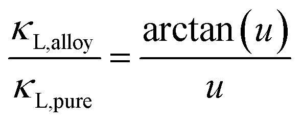 | (3) |
 | (4) |
 | (5) |
 | (6) |
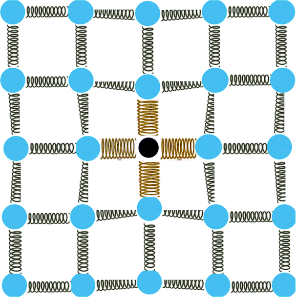 | ||
| Fig. 1 Illustration of a substitutional point defect in a crystalline lattice. The defect brings a different atomic mass, different bonding strengths with its neighbouring atoms, and strains to its surrounding lattice; all have an impact on thermal conductivity in solid solutions where large numbers of substitutions are present. | ||
G in eqn (6) is a ratio between the contrast in bulk modulus (ΔK/K) and that in the bonding length (ΔR/R). The relationship between bulk modulus and the volume of the unit cell has been studied for a lot of compounds. For instance, see Anderson's study76,77 on minerals of different types. A general trend exists among similar compounds: KVG = constant (Fig. 2). From an ln![[thin space (1/6-em)]](https://www.rsc.org/images/entities/char_2009.gif) K vs. lnV plot, it was found (when ΔK and ΔR are small, G is approximately three times the slope) that G = 4 for covalent IV and III–V structures, and more ionic II–VI and I–VII structures G = 3. The value of G should be based on material systems. For Pb chalcogenides, we suggest the use of G = 3.
K vs. lnV plot, it was found (when ΔK and ΔR are small, G is approximately three times the slope) that G = 4 for covalent IV and III–V structures, and more ionic II–VI and I–VII structures G = 3. The value of G should be based on material systems. For Pb chalcogenides, we suggest the use of G = 3.
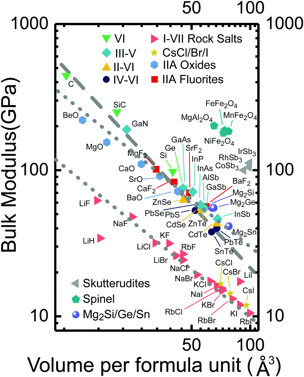 | ||
| Fig. 2 The log–log plot of the bulk moduli of different compounds versus volume per formula unit. Linear trends are found among similar compounds, the slope is approximately −G/3. The plot was reproduced based on Fig. 1 in ref. 77. Added data are from ref. 78 (lead chalcogenides), ref. 79 and 80 (skutterudites), Springer Landolt–Bornstein Database, and ref. 81 and 82 (II–VI, some III–V, and Mg2X). The dashed line has a slope of −4/3. The dotted line has a slope of −1. | ||
With all parameters in eqn (6) determined, the value of ε could be calculated for any binary compounds. For PbTe, PbSe and PbS, ε was calculated to be 100, 110, and 150, respectively. For PbTe-based systems, ε was previously suggested to be 65 by Alekseeva,83 which was obtained from fitting experimental results. This value has been used in lots of studies. We suggested the use of 100 as it has a clear physical basis and the modeling results remain reasonably consistent with experiments. On applying eqn (6) to different systems, we found that for Si1−xGex and Ga1−xInxAs, the calculated ε was very close to those from fitting,75,84 whereas for Mg2Si1−xSnx, a significant discrepancy was seen (23 from fitting85vs. 67 from calculation). In compounds with mixed ionic and covalent bonding character, uncertainty around the choice of atomic or ionic radii when defining the strain scattering term can further confound predictions.86 Bearing some uncertainty, the thermal conductivity of binary (pseudo-binary) solid solutions can be predicted with Klemens’ method, with no fitting parameter needed.
Abeles has suggested75 that when there is more than one type of substitutional defect, eqn (5) should be generalized to eqn (7), where i indexes the species that can occupy the lattice, including the host atom and any impurity defects:
 | (7) |
Yang et al. introduced87 another method, which is widely adopted and successful when applied to complex structures like skutterudites. In this method, Γ has two parts ΓM and ΓS, representing the mass fluctuation and strain fluctuation (for a case with n sublattices, and each sublattice has two different atoms ‘1’ and ‘2’, see ref. 73 and 87 for detailed descriptions):
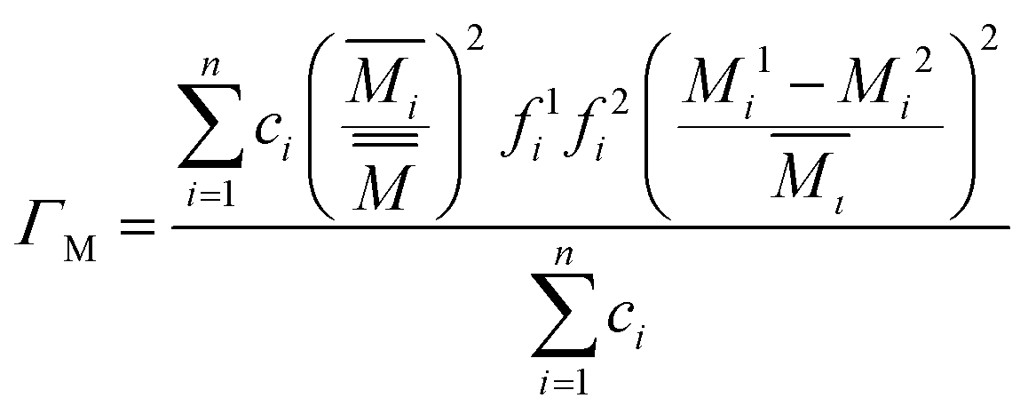 | (8) |
 | (9) |
 is used in eqn (9) on strain fluctuation. A probable rationale is that the vibrations of heavier sublattices have larger impacts on the overall vibrational modes of the structure, and thus perturbations on each sublattice should be weighed in accordance with this term, although no clear reasoning was explicitly provided.
The two treatments appear more different than they actually are. The most general formulation for the point defect scattering parameter of a polyatomic lattice (i.e. multiple sublattices) with an arbitrary number of defects was first presented by Berman, Foster, and Ziman for isotope scattering.89 Here, the scattering parameter Γ has the basic form of the averaged atomic mass variance in the lattice divided by the squared averaged atomic mass. The form below, extended to include strain fluctuations, is discussed in detail in eqn (10):73
 | (10) |
![[M with combining macron]](https://www.rsc.org/images/entities/i_char_004d_0304.gif) or V signifies a configurational average over all arrangements of the alloy. The angular brackets (〈〉) signify a stoichiometric average over all the elements in the formula unit. More explicitly,
or V signifies a configurational average over all arrangements of the alloy. The angular brackets (〈〉) signify a stoichiometric average over all the elements in the formula unit. More explicitly,  is given as follows:
 | (11) |
Most implementations of Γ, as detailed above, are based on “per atom” quantities, with the perturbation defined by atomic mass or radius variances and the defect volume Ω defined as the volume per atom. However, several texts, including the original work of Klemens,68 define Γ instead in terms of “per unit cell” quantities, which quantify the perturbation in terms of the mass and volume change of the primitive unit cell when it is occupied by a specific population of substitutional defects.67 This treatment is in keeping with a monatomic lattice approximation, in which all atoms in the primitive unit cell are effectively summed together into a single, vibrating mass. It is shown73 that either formulation will provide equivalent results, as long as the user is consistent in using “per atom” or “per unit cell” definitions. Several discrepancies exist in model results reported in the literature when parameter definitions have a mixed basis. Often eqn (10) is defined in terms of atomic masses and radii, but then Ω in eqn (4) is defined as the volume of the unit cell, leading to an overestimation of the thermal conductivity reduction due to alloy scattering.90–93
In several cases, this literature discrepancy has obscured the unique scattering characteristics of off-stoichiometric defects, like vacancies and interstitial atoms. In the vacancy and interstitial cases, the removal or addition of bonds leads to a large potential energy perturbation and additional scattering. A simple Klemens model based on the virial theorem relates the potential energy perturbation to the average atomic mass in the solid (〈〉). Therefore, in this model, the scattering parameter can be determined solely using the ΓM term when ΔM = Md + 2〈〉, where Md is the missing/added mass of the vacancy/interstitial defect. In practice, vacancy and interstitial defects can have about 10 times the scattering strength (Γ) of a simple, substitutional defect.94,95
2.2 Charge carrier mobility
Regardless of how effective point defects are in the scattering of phonons, they cause the scattering of charge carriers as well. For isovalent substitutional defects, the atomic site is not charged. Scattering is caused by perturbations to the periodic lattice potential and is called alloy scattering.To briefly explain how the relaxation time is determined, consider a lattice containing only two types of atoms A and B, and define the average lattice potential in a disordered system:
| Ū = xUA + (1 − x)UB | (12) |
| He-alloy,A = UA − Ū = (1 − x)ΔU | (13) |
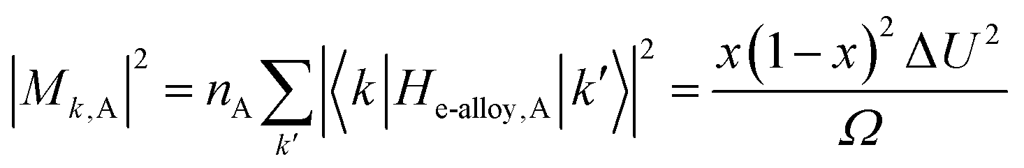 | (14) |
 | (15) |
 | (16) |
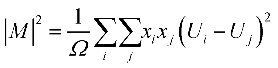 | (17) |
The first explicit expression of relaxation time τalloy was developed by Harrison and Hauser101,102 for nondegenerate III–V semiconductors. We used this expression in previous works; τalloy for a parabolic band is given by
 | (18) |
The alloy scattering potential ΔU, following the simple derivation, is the offset of lattice potentials between substitutional atoms and the atoms being substituted. Unfortunately, based on lead chalcogenides, we found that none of the potential offsets obtained directly from another method can explain the experimental mobility reduction in solid solutions. Historically, Brooks109 suggested using the band gap difference between the 0% and 100% substituted compounds. This was later found to provide inaccurate values, whereas, the difference in electron affinity (hence the position of band edges relative to vacuum level) is a better measure.96,110 This is clearly not supported by results from the PbTe–PbSe or PbSe–PbS system: in each case, the conduction band offset is about 0.1 eV, whereas ΔU from the mobility data is around 1 eV (Fig. 3a and b). Band alignments were calculated via DFT for coherently embedded nanoscale clusters;108,111–113 these cannot be applied in the case of point defects. In cases where near-perfect band alignment was found for nano-clusters,108 experimental results with solid solutions107 have shown significant alloy scattering (Fig. 3c).
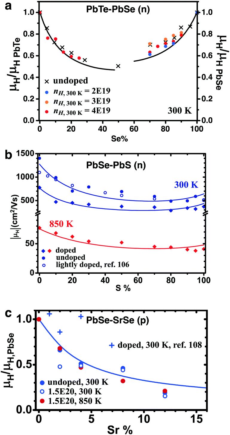 | ||
| Fig. 3 Mobility reduction due to alloy scattering in lead chalcogenide solid solutions. (a) n-Type PbTe–PbSe, ref. 74. (b) n-Type PbSe–PbS, ref. 105 and 106. (c) p-Type PbSe–SrSe, ref. 107 and 108. In each case, the comparison was made among samples with similar carrier densities. Solid lines were calculated using combined carrier scattering mechanisms, see ref. 105 and 107 for modelling details. No fitting parameter was used. | ||
So far, ΔU can only be found as a fitting parameter, and predicting mobility changes in solid solutions is still a goal to reach. Nonetheless, a qualitative link between the band position offset and ΔU might be justifiable: ΔU is around 1 eV in n-type PbTe–PbSe and PbSe–PbS, and 3 eV in PbSe–SrSe. The band position offset is around 0.1 eV for the former two cases and 0.8 eV for the latter. Further study in p-type PbSe–PbS would be helpful; since the valence band offset in this case is very small (0.03 eV), ΔU much less than 1 eV, and a minimum mobility reduction are expected. We note here that a similar discrepancy was seen in the coefficient Ξ for deformation potential scattering: from fitting mobility data Ξ in lead chalcogenides were found114 to be over 20 eV, whereas those from calculation115 were no more than a few eV.
Often, disorders from point defects in lead chalcogenides are not ‘beneficial’. However, studies in other material systems, for example, many half-Heusler compounds, have demonstrated that point defects (iso-valent substitution or doping) are capable of reducing thermal conductivity without a heavy penalty on carrier scattering.117–120 There is no guideline to predict what substitutions, or which systems can benefit from disorder. To shed some light on this, we observed that in lead chalcogenides, the strain contrast has a large contribution to the thermal conductivity reduction (ε from eqn (6) is large in these cases), whereas in half-Heuslers the strain contrast is almost negligible117,118 (especially, when between a period-5 and a period-6 element). The more fundamental reason could be that the bands in lead chalcogenides are from more-overlapped, less-hybridized p-orbitals of cations and anions (hence, small effective masses, high mobilities), which are sensitive to interatomic distance changes. In contrast, bands in half-Heuslers are from less-overlapped, highly-hybridized d-orbitals (hence, large effective masses, low mobilities), which are insensitive to changes in the local atoms.
Therefore, selecting an alloying element that has a large mass difference and a small atomic size difference with the host atom should be more likely to generate a beneficial disorder. Such candidates are more likely to be found when both alloying and host atoms are transition elements. The lanthanide contraction leads to a small covalent radius difference between the period-6 elements (post-lanthanides) and their isoelectronic period-5 counterparts. Following this, we have found a strategy (Fig. 4) particularly suitable for half-Heusler compounds containing transition metals ranging from periods 4 to 6: n-type Zr1−xHfxNiSn, p-type (Nb1−xTax)0.8Ti0.2FeSb, and n-type (Zr1−xHfx)0.88Nb0.12CoSb are all successful examples.117–120
 | ||
| Fig. 4 (a) The effect of alloy scattering on the phonon and charge carrier transport. An alloying atom that has different mass contrast but a similar radius to the host atom could create strong phonon scattering with relatively low alloy scattering potential. (b) Covalent radius difference between the period-5 transition metal and their isoelectronic period-4 and period-6 counterparts. Rcx indicates the covalent radius of period-x elements. The data are taken from ref. 116. The effects of period-6 elements Hf and Ta on the κL and μ for n-type ZrNiSn (c) and p-type NbFeSb (d). The data were taken from ref. 117, 118, and 120. κL0 and μ0 denote the lattice thermal conductivity and carrier mobility of the unalloyed compound, respectively. | ||
Another successful example of material engineering that reduced thermal conductivity without impairing carrier mobility is from in skutterudites with filler atoms in structural voids.121,122 Filling by one or multiple species of atoms is a method to obtain a high figure of merit in skutterudites. It is possible to have a minimum impact of fillers on carrier mobility, while introducing strong phonon scattering. Having a covalent ‘framework’ and weakly bonded ionic atoms is responsible for strong phonon scattering and low thermal conductivities in many structures, such as perovskites: oxide perovskites tend to have relatively low thermal conductivities123–126 (given their light atomic constituents). In the hybrid halide perovskites, this effect combined with the rather anharmonic covalent framework resulted in extremely low, amorphous-like thermal conductivities,127–129 even in single-crystals.130–132
To end this section, we point out that for most of the well-known successful examples of thermoelectric solid solutions, a major contributor to the high thermoelectric performance could be other factors such as the change in band structures. One of the reasons why Bi2Te1−xSex and Bi2−xSbxTe3 have better performance than Bi2Te3 is that band gaps in these alloys are larger, thus thermal excitation of minority carriers is inhibited. The change in defect chemistry133 and carrier concentration is another factor such that no additional doping is necessary. Band convergence happens in systems (Fig. 5) such as17,24,134–139 Bi2−xSbxTe3, Bi2SexTe3−x, Si1−xGex, PbTe1−xSex, Mg2Si1−xSnx, or Mg3Bi2−xSbx (different explanations should be noted140,141), so much so that in most cases (except for Si1−xGex), the optimum solid solution composition is consistent with what is required for band convergence.
 | ||
| Fig. 5 Band convergence in thermoelectric solid solutions. (a) Hole pockets of Bi2−xSbxTe3 and (b) schematic valence band positions with different compositions, from ref. 134. (c) Hole pockets in PbTe and (d) schematic valence band positions at different temperatures in PbTe1−xSex, from ref. 137. (e) Schematic band positions of Mg2Si1−xSnx, from ref. 138. Used with permission, Copyright the American Physical Society. (f) Schematic band positions of Mg3Sb2−xBix, from ref. 24. | ||
3. Systems with multiple bands
Thermoelectrics often demonstrate better performances when they take advantage of complex band structures. Symmetry-imposed degeneracy of multiple carrier pockets is seen in most high-performance systems. In other cases, materials have benefited from the presence of additional bands with small energy offsets from the primary conducting bands. Enabling band convergence,107,137,142 where the edge of different bands came to the same energy, has been a dependable strategy to achieve higher zTs.The maximum possible thermoelectric properties of a two-band system have been discussed in several studies.143 Some are for electron–hole systems144,145 as many thermoelectrics are narrow bandgap semiconductors. Consider a system with two bands having a reduced energy offset Δ (= ΔE/kBT), and using a simple mixed conduction equation for each transport property, we have:
 | (19) |
 | (20) |
 | (21) |
 | (22) |
 | (23) |
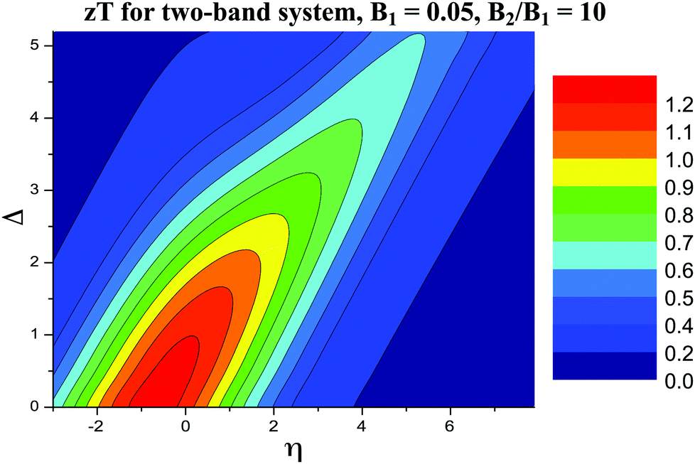
Fig. 6 and 7 present the zT of a hypothetical two-band system (both are parabolic). In Fig. 6 we take B1 = 0.35, which is about the quality factor of the L valence band146 in PbSe, and in Fig. 7B1 = 0.7, which is about that of the L conduction band146 in PbSe. The value of B2 is allowed to change within a reasonable range based on known quality factors. We consider 0.17 to be the lower bound for meaningful contribution to zT, whereas 1.4 is almost unrealistically high based on known examples.
 | ||
| Fig. 6 Modeled zT of a two-band system with the two bands separated by reduced energy, Δ. The quality factor for the first band B1 = 0.35. (a)–(d) Cases with different quality factors B2 for the second band. | ||
 | ||
| Fig. 7 Modeled zT of a two-band system with the two bands separated by reduced energy, Δ. The quality factor for the first band B1 = 0.7. (a)–(c) Cases with different quality factors B2 for the second band. | ||
Note that we have neglected a potential adverse influence on carrier mobility when multiple bands come closer: the effect of inter-band/valley scattering. It is reasonable to expect that the optimum zT in a two-band system would be lower than expected from the simple analysis above, which assumes no inter-valley scattering. In simple terms, the question is the strength of inter-valley scattering as compared to intra-valley scattering.59 If there is a symmetry requirement forbidding inter-valley scattering, there is a clear benefit. However, even when the scattering is allowed, there is little reason to doubt that a higher B and zT would result.
Consider inter-band scattering when the initial and final states belong to different pockets with their extrema at the same k point. The inter-band scattering is very similar to intra-band scattering because of the small change in the wave vector. One such example is the multi-band system of Mg2X (X: Si, Ge, Sn). An expression of relaxation time was suggested147,148 and an inter-band deformation potential D was introduced. In principle, D can be determined if both functional forms of the two band states are known; this is by no means easily available information. Experimentally, it is impossible to tell the inter-band processes from the normally discussed intra-band processes since they have the same energy and temperature dependence. First-principles calculation of the electron–phonon interaction would be the only method to study this. In general, this type of multi-band system tends to see increased inter-band scattering as two bands move close. It is now known that in certain systems,149 the convergence of bands is not beneficial due to increased carrier scattering. Nonetheless, in other systems like Mg2X (X: Si, Ge, Sn), the convergence is beneficial and the inter-band scattering was reported as insignificant.147
The inter-valley scattering is a little different when the two pockets have extrema at different k points. Since a large change in the k vector is needed, this process resembles that of the optical phonon scattering and is inelastic in nature,150–153 which is distinguishable from intra-valley deformation potential scattering processes. The best-known example of inter-valley scattering is perhaps in n-type Si where inter-valley scattering was found to be twice as significant as intra-valley scattering.151,154–156 However, several more recent results157–161 have indicated that the inter-valley scattering is important but not greater than intra-valley scattering. Overall, there have been only very limited examples (ref. 162 which is a theoretical study) where the convergence of multiple valleys has failed to improve the thermoelectric performance.
As long as inter-band/valley scattering would not completely offset the benefit from converging multiple bands, the following principles can be concluded (the dominant scattering mechanism is still deformation potential scattering):
1. The optimized zT is determined only by quality factors of both bands and their offset, not the individual band characteristics, such as effective mass.
2. The quality factor of the first band sets the baseline for zT. The second band adds its contribution depending on the offset between them; the smaller the offset, the larger the contribution. If a system has a first band with a low-quality factor, its zT will not be high unless a better second band takes over.
3. Depending on the ratio B2/B1, the second band starts to contribute when Δ is below ∼2 (small B2/B1) to ∼4 (large B2/B1). On the other hand, two bands with Δ ≤ 1 are almost as good as converged (though which one comes first matters). More studies are needed to understand whether the inter-band/valley scattering intensity has notable changes within such a range of Δ.
4. In most cases, the maximum zT is achieved only at one η, which is close to the edge of the first band (slightly below, for a conduction band), regardless of B2. A good strategy should always be reducing Δ, instead of excessive doping to let η ‘reach a better band’. This is consistent with our conclusion regarding resonant doping in the next section, that the resonant level should be close to the band edge.
5. Only for extreme B2/B1 ratios, the optimum η moves away towards the edge of the second band, and the maximum zT is found when η is near the edge of the second band. B1 is very small in this case (Fig. 8 and 9). This is likely the case when the first band is an in-gap defect band.163 Even though the optimum η followed the second band, the first band still leaves its negative impact on zT.
 | ||
| Fig. 8 Modeled zT of an extreme two-band (hypothetical) system with the two bands separated by reduced energy, Δ. The first band is set to be a very poor one with B1 = 0.05 (zT below 0.2), while the second band has a decent B2 = 0.5. | ||
 | ||
| Fig. 9 The optimum reduced chemical potential η in two-band systems with different Δ and B2/B1, for different B1: (a) 0.01, (b) 0.1, (c) 0.3, (d) 1.0. Dashed lines in (c) and (d) draw limits, where B2 to their right is very unlikely. | ||
6. When the two bands are close (Δ < 1) the optimum η slightly shifts toward the second band. This shift is less than 0.5kBT, even when the second band has a B factor twice as high. The optimum η for a two-band system is approximately the same as that for the first band alone. The carrier density needs to be properly increased to keep the same η.
This discussion so far is simply based on numerical simulation. Nonetheless, we can consider a few real examples where experimental findings reflect such principles:
3.1 La3−xTe4
La3−xTe4 is an excellent n-type material164 at high temperatures (T > 1000 K). Band structure calculation165 indicated two sets of conduction bands separated by about 0.3 eV (Fig. 10a), which is equivalent to Δ = 2.8 at 1273 K. Fermi distribution can create finite occupancy of the second band even at lower temperatures (400 K, Fig. 10b) with composition control (doping). However, as suggested by our discussion above, at this value of Δ, the second band would have limited contribution to the overall performance. La3−xTe4 has decent zT at lower temperatures, as well with optimized zT > 0.6 at 700 K, suggesting a decent quality factor B1 for its first conduction band. Thus, if we assume the first conduction band has a B1 that scales with T, at 1273 K the observed maximum zT of 1.1 matches our expectation without the contribution from a second band. The optimum carrier density was found around 2 to 4 × 1020 cm−3, consistent with the expected doping level for a DoS effective mass of the first band (1.4 me). This further suggested that no significant number of carriers populated the second conduction band. Thus, even though La3−xTe4 is a system with two conduction bands, it is likely that the second band has limited contribution to the material's high zT.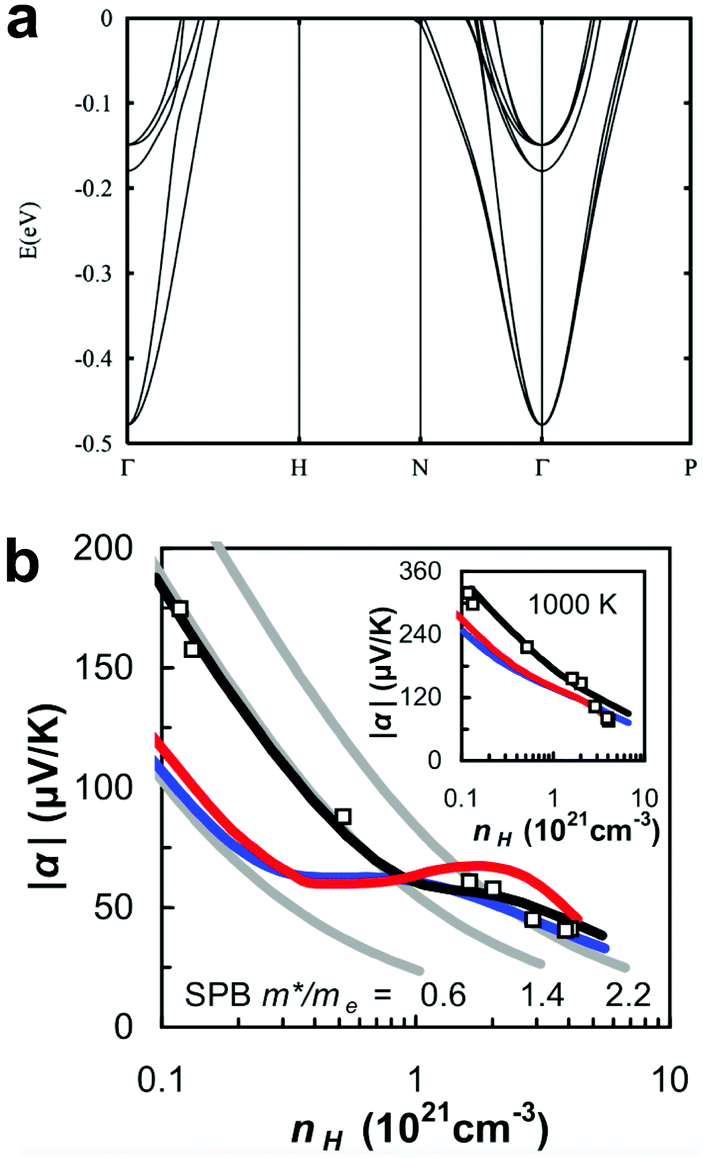 | ||
| Fig. 10 (a) The calculated band structure of La3−xTe4 close to the conduction band minimum, showing secondary bands around 0.3 eV above the primary band. (b) The Pisarenko relation at 400 K (inset 1000 K) shows an increase in the effective mass as carrier density increases. The red curve is from first-principles calculations based on the calculated band structure. The blue curve is from a multi-parabolic band model with effective masses and band offsets from first-principles calculations. The black curve is from a semi-empirical multi-parabolic band model, where the effective mass of the first band was adjustable and set to 0.844. From ref. 165, used with permission, Copyright the American Physical Society. | ||
3.2 CoSb3
CoSb3 has two conduction bands. Historically, Sofo and Mahan166 found from the calculated band structure that CoSb3 has a non-parabolic Kane band and a triply degenerate parabolic band at the Γ point. A previous study50 using optical absorption (300 K) identified a second conduction band off Γ at 0.08 eV above the primary band edge (corresponding to Δ = 3.1 at 300 K, and 1.2 at 800 K, as shown in Fig. 11b and d). This second conduction band has a complex Fermi surface (Fig. 11c), a very large DoS effective mass, a high equivalent degeneracy Nv, and a quality factor B2 that is likely comparable or even better than the first one (we estimated B1 to be around 0.4 at 800 K). Different from La3−xTe4, the small Δ makes the second band influence perceptible even at room temperature: the observed effective mass from the Seebeck coefficient steadily increases with carrier density.9 At a high doping level of 5 × 1020 cm−3, the Seebeck coefficient was still9 around −100 μV K−1. Assuming the same Δ, we could estimate the optimum zT at 800 K to reach 1.2 (see Fig. 6b). Better yet, temperature-dependent absorption50 measurements confirmed that Δ decreases with temperature and the two sets of bands converge at around 800 K. The convergence could potentially bring maximum zT to 1.5 at 800 K. | ||
| Fig. 11 (a) Seebeck coefficient (S) versus Hall carrier concentration (nH) at 300 K for n-type CoSb3. The solid black line from the multi-band model. Orange and red dashed lines show single parabolic band behavior with masses equal to the two individual conduction bands. (b) The electronic band structure and density of states (DOS) for CoSb3. (c) The Fermi surface for a Fermi level 0.11 eV above the conduction band minimum showing the 12 pockets of the second conduction band CB2. (d) Room-temperature optical absorption measurements showing two distinct transitions. From ref. 50. | ||
Experimentally, single-filled CoSb3 achieved zT = 1.2 at 800 K. This value is lower due to the narrow bandgap of CoSb3 (at 0.23 eV at 300 K). In fact, based on Fig. 9c, the optimum η with converged bands is between −0.5 to −1.0, suggesting that the Seebeck coefficient should be between −240 to −270 μV K−1 when zT is maximized. Experimental values from different studies are around −180 μV K−1, which is an indicator of the valence band influence.
3.3 Bi2Te3
Bi2Te3 is an outstanding system due to its inherently low lattice thermal conductivity and complex conduction and valence band Fermi surfaces. Both its conduction band side and valence band side Fermi surface have two (three) sets of valleys emerging at different energies167,168 (Fig. 12). The primary valence band is six-fold degenerate. The edge of the second set of six valleys has an offset of 0.03 eV (Δ = 1.2) from the band edge. At even higher energies, a total of 12 pockets merge around Z point forming a ring structure. On the conduction band side, the primary conduction band is also six-fold, the second set of two pockets along the Z–Z line emerge at 0.05 eV (Δ < 2) from the band edge. Lastly, at a higher energy of 0.08 eV (Δ < 3.1), another set of six valleys begin to emerge. | ||
| Fig. 12 Valence and conduction band Fermi surfaces of Bi2Te3 at different energies; from ref. 167. | ||
At 300 K, transport in both p-type and n-type Bi2Te3 will have notable influence from the additional pockets. Nonetheless, if we assume that the primary bands dominate transport processes, we can find167 that the conduction bands have a slightly higher quality factor BC = 0.26, while BV = 0.2 (electrons have higher mobility, effective masses are identical). This is reflected in the best zTs observed167 for Bi2Te3: 0.8 for the n-type and 0.5 expected for the p-type.
To achieve higher zTs, different alloys are used: Bi2−xSbxTe3 and Bi2Te3−xSex. The alloys have larger bandgaps and thus inhibit the bipolar effect in Bi2Te3. Isovalent substitutions also changed the defect chemistry, which brought convenient control of carrier densities. Point defects further reduced the lattice thermal conductivities, and while doing so, did not cause a reduction in mobilities. In fact, the mobilities in Bi2−xSbxTe3 might have increased.
It turns out solid solutions in both cases changed the offsets of different carrier pockets, causing the convergence of different pockets.169 In Sb2Te3, the order of the first and second set of hole pockets was flipped170 as compared to Bi2Te3. In their alloys, the two sets converged around the composition of Bi0.25Sb1.75Te3 (a larger effective mass171,172 at this composition is also an indicator). In Bi2Se3, the primary electron pocket is173 the one along Z–Z; alloying with Bi2Te3 allows these two pockets to converge with the six pockets in Bi2Te3 around the composition172 of Bi2Te2.7Se0.3.
Assuming it is comparable to its counterpart167 in Sb2Te3, the second set of six hole pockets in Bi2Te3 should have a quality factor (0.20, take κL same as Bi2Te3) that is close to the first set (BC in Bi2Te3). On the other hand, assuming the two pockets along Z–Z in Bi2Te2.7Se0.3 have characteristics from Bi2Se3, we can see that they have a much lower quality factor (0.09, take κL same as Bi2Te3). While convergence happened in both alloys, different valleys were converged. The higher quality factor of the second band made the p-type Bi0.25Sb1.75Te3 the one174–177 with higher zT, while in binary Bi2Te3 it was the opposite.
Additionally, from the modeling above, when the two bands have similar B, zT will be close to the maximum when the two are very close, regardless of which one is the primary. Thus, we expect in p-type alloys that the maximum zT is not sensitive to small changes in alloy composition, given that carrier densities are properly tuned; this was observed experimentally.178,179 On the other hand, for n-type alloys, we know that (a) smaller Δ are required for the second band to affect overall zT, (b) zT of a two-band system is primarily determined by the first band. Thus, we expect the maximum zT to be more sensitive to composition changes, especially on the Se-rich side (when the low-quality band becomes primary). Again, this was observed experimentally.180,181 If a pseudo-ternary system can be found, which also converges the additional six electron pockets, notably higher zTs can be expected for n-type alloys.
4. Resonant doping
In thermoelectrics, dopants are point defects that provide free charge carriers thus shifting the position of the Fermi level. Often, this is considered as (approximately) their only impact on the material's transport properties (with exemptions for very heavy doping). The resonant dopants are a special type of dopant, which, in addition to providing free carriers, interact with conducting bands, leading to unique transport behavior.182–187 The success of resonant doping is well-known188,189 in Tl-doped PbTe and In-doped SnTe, and the enhancement of effective mass m* as seen from the higher Seebeck coefficient in the Pisarenko (S vs. n) relation. More recent studies suggest that resonant doping exists in more systems such as Bi2Te3,187 GeTe,190 half-Heuslers,191,192 As2Te3,193 and Zn4Sb3.194In classic semiconductor physics, the dopants that provide free carriers are depicted by discrete defect levels below the edge of the density-of-states of the conduction band (taking donors as an example, Fig. 13a). The defect levels are so-called “hydrogen-like” levels, meaning they are not from a specific atomic orbit from the donor, but effective ones to account for the coulombic interaction between the positively charged ion cores and the free electrons. These large polaron levels are below the band minimum so carriers are free only when the orbits from neighboring defects overlap or activation energy (thermal or electromagnetic) is provided to dissociate them from cores. In heavily doped semiconductors, the discrete defect levels interact with each other, become “band-like”, and overlap with the conduction band. This results in metallic transport behavior and donors are always mobile.
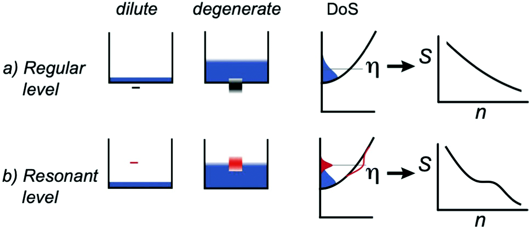 | ||
| Fig. 13 An illustration of hydrogen-like levels from (a) regular dopants and (b) resonant dopants (ref. 195). In dilute cases, these levels are treated as non-interacting, discrete levels, whereas in degenerate cases, these levels form bands. In the case of regular dopants, the defect levels do not cause changes to the total density-of-states. In the case of resonant dopants, the additional density-of-states from defects is Lorentzian and interacts with the continuous band states, distorting the total density-of-states. | ||
In the case of resonant doping, the “hydrogen-like” levels from dopants are found above the minimum of the conduction band density of states.186 With energy relaxation, electrons will dissociate from these states forming free carriers in the conduction band. Different from regular dopants, resonant defects continue to interact with carriers (beyond normal Coulombic interactions that give rise to ionized scattering), which depends heavily on carrier energy and is strongest when the defect level aligns with the Fermi level (Fig. 13b). This interaction causes carriers to ‘resonate’ between continuous band states and the ‘discrete, defect states’186,196 (keep in mind they are not actual atomic states, and the carriers do not actually transit between different states). It is worth noting that all known examples of resonant dopants are elements that have multiple valences.185,197–199 Although there is no definitive evidence yet, that multiple valences (such as Tl1+ and Tl3+) coexist in these cases (some recent study218 did suggest existence of mixed valence, in contrast with previous studies such as ref. 219,220).
Identification of resonant behavior is in most cases based on an increased effective m* either by density-of-states DFT calculations or increased Seebeck coefficient over the regular carrier density dependence (Pisarenko relation). In principle, strong energy-dependent resonance leads to Fermi level pinning, which is seen as the saturation of carrier concentration measured by the Hall effect when the dopant concentration changes. Additionally, upon sufficient co-doping or counter-doping with a regular dopant, the carrier concentration could increase or decrease again (un-pinning). The pinning and un-pinning behavior, combined with Seebeck coefficients, serve as a more definitive indicator of resonant doping experimentally. As seen in Fig. 14, the measured carrier densities showed clear pinning and un-pinning in PbTe with resonant dopants of Tl (ref. 200, 14b) and Ti (ref. 197, 14c), and PbSe with resonant dopants of Tl (ref. 195, 14a); the same is likely although not as clear in SnTe with resonant dopants of In (ref. 201, 14d).
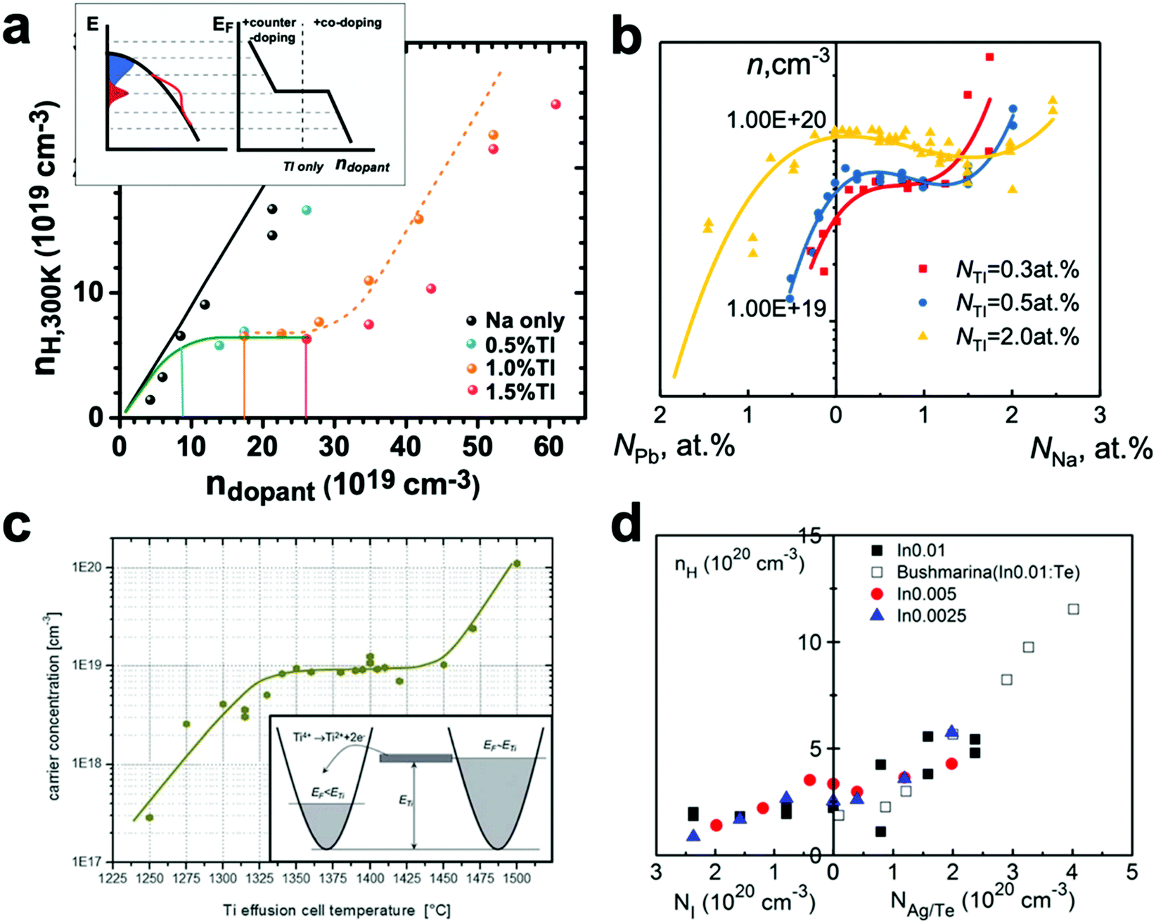 | ||
| Fig. 14 Fermi level pinning observed experimentally in different resonant systems. (a) Tl in PbSe codoped with Na; the top inset is a sketch of how the Fermi level changes with doping in the Tl:PbSe case. (b) Tl in PbTe at 77 K, codoped with Na, or counter doped with Pb, reproduced using data from ref. 200 (c) Ti in PbTe, from ref. 197; the Ti effusion cell temperature is proportional to the Ti concentration. In this, unpinning of the Fermi level is possible without the use of another dopant. Used with permission, Copyright the American Physical Society. (d) In in SnTe co-doped with Ag or counter-doped with I. From ref. 201. The pinning of the Fermi level, in this case, is not as clear. Used with permission, Copyright the American Institute of Physics. | ||
Resonant doping could be beneficial, however, optimization is necessary to reach the best possible thermoelectric performance. Using Na and Tl co-doped PbSe as a platform, a descriptive model was proposed195 so carrier density and temperature-dependent properties can be modeled.
In this model, only the density-of-states distortion from resonant states was taken into account. Additional resonant scattering mechanisms were not considered, for the reasons discussed in ref. 186 and 195. The change in the density-of-states affects transport properties either through the change in carrier group velocity, or the change in the scattering probability, so each transport property can be expressed.
The distortion of DoS was described195 by an additional Lorenzian term184 to the total DoS:
 | (24) |
To express the transport properties, the carrier group velocity has to be determined. ‘Resonating’ between the band states and localized states would reduce the group velocity of carriers; to capture this, the following relations were considered:
 | (25) |
 | (26) |
 | (27) |
Note that three parameters were introduced in this model: Eres, Γ, and H. Eres can be determined by solving for Eres= EF using the ‘pinned’ carrier concentration. For Γ and H, it is not clear if they can be determined from experiments. In the previous work they were taken as adjustable parameters. All three parameters are set as constants for a given resonant system. Fig. 15 illustrates how each of them affects the Seebeck coefficient and mobility at 300 K.
 | ||
| Fig. 15 Modeled transport properties at 300 K in PbSe, from ref. 195, with each of the three parameters changed to illustrate their influence on (a), (c) and (e) the Seebeck coefficient, and (b), (d) and (f) the Hall mobility. The default values of these parameters are Eres = 0.125 eV, Γ = 0.04 eV and H = 0.08. Each parameter is then allowed to change one at a time. | ||
With reasonable accuracy, the modeled carrier density dependence of the Seebeck coefficients and mobility were consistent with experimental results in the applicable temperature range. Although similar calculations186 (same scattering mechanism, DoS from KKR-CPA) had successfully described the Seebeck coefficient in PbTe doped with Tl, the work on PbSe provided a complete picture that describes both Seebeck coefficients and carrier mobility, as well as their temperature dependence.
Based on this model, some general guidelines regarding resonant doping can be summarized:
(1) Resonant doping leads to stronger mobility reduction and, therefore, is not always beneficial for thermoelectrics.202 However, a moderate increase (10–20%) in the power factor under optimum n is possible in some cases. Tl doping in PbTe is the best-known example of resonant doping but the zT was not higher than PbTe doped with regular dopants. Tl doping in PbSe is not beneficial for zT. So far, the only case189 to achieve higher zT than regular cases with a resonant dopant is In in SnTe.
(2) The impact of ‘resonance’ can be seen at different temperatures (assuming the nature of the defects does not change, only the result of DoS distortion). The unique ‘hump’ of the Seebeck coefficient within a certain carrier density range may not always be seen. In many cases, the impact on the Seebeck coefficient is similar to an increased effective mass.203
(3) Further tuning of the carrier density with a regular dopant is likely needed. Optimization should involve co-doping or counter-doping.
(4) The optimum position for a resonant level/band is close to the continuous band edge, with a small offset into the band. This conclusion is consistent with the study using tight-binding plus transport property modeling.204
(5) The DoS distortion causes the zT to peak at higher Seebeck coefficients,205 whereas for systems approximated by a single parabolic band and deformation potential scattering, zT tends to peak48,206 when the Seebeck coefficient is around 250 μV K−1. This could be favorable for certain device applications.207
This is an example of how transport property modeling can help to guide material optimization, which would otherwise be tedious to study on a trial-and-error basis. This is true even when two parameters in the model are obtained from fitting, and the modeling still needs a good amount of experimental input.
5. Outlook
Thermoelectrics often have better performance when they take advantage of complex physical phenomena. The challenge is to characterize complex phenomena in a manner that can be engineered using the simple tuning parameters, composition, and processing conditions, available to synthetic chemists. The analytic models discussed here represent simplifications that describe the essential physics of the complex phenomena using a few scalar parameters that can be changed with synthesis conditions. Although not an exact theory, the formulations are based on the correct physics so that they should characterize a large fraction of the effect in a way that can be interpolated and extrapolated, perhaps more accurately than a machine learning algorithm, for example.Many of the parameters used in these models are obtained from fitting experimental measurements. Often they cannot be determined in advance using other properties; for instance, the alloy scattering potential ΔU, which we only know qualitatively where it comes from and can only guess its order of magnitude. For some of the parameters used to characterize resonant scattering, even such a qualitative relation is not clear. In the case of point defects on thermal conductivity, we argued that a simple, analytical approach is possible where all parameters can be determined from observable properties. This is the case mostly for mass contrast or simple structures like Si, Ge, and rock-salt lead chalcogenides. More studies on diverse and complex materials are needed for such models to be predictive. Although easily interpolated to similar systems with small compositional variations, it is difficult to extrapolate by predicting the parameters in complex materials without full experimental characterization.
While we currently only use the fitting of experimental results to obtain these parameters, the rapid advances of computational methods may revolutionize the process. It is tedious experimental work to prepare and exactly measure the same samples with only one synthetic parameter changed. However, such a computational, virtual experiment, is now relatively easy, even if not exactly applicable (e.g. approximations to the physics or missing microstructural effects). This provides an immense opportunity for theory and experiment to collaborate toward an engineering goal.
One must keep in mind that the analytical models are essentially isotropic, spectral averages of various related physical phenomena. It should not be surprising when parameters that fit experiments differ from values determined computationally or even other experiments. The deformation coefficient Ξ of lead chalcogenides can be very different from calculated values (for example, ref. 115). This is at least partly because of other carrier scattering mechanisms,208 such as deformation potential scattering from optical phonons,209–211 inter-valley scattering, and potential scattering from ionized impurities,212 which are not distinguished from the often-called ‘acoustic phonon’ deformation potential. The realization, for example, that optical rather than acoustic phonons are primarily responsible for temperature-dependent electron scattering in complex crystals leads us to think of the deformation coefficient Ξ as an effective parameter for phonon scattering (rather than just acoustic phonons). Similarly, the alloy scattering potential ΔU is more complicated than just electronegativity or work function differences. Additionally, different crystal symmetry and atomic coordination could make the analytical equations slightly different. Overall, the basic modeling approach is a compromise between simplicity, generality, and accuracy.
Compared to inorganic semiconductors, thermoelectric transport properties in organic or composite semiconductors are very poorly understood. Taking organic semiconductors as an example, historically, researchers used theories such as variable range hopping213,214 based on amorphous inorganic semiconductors to explain general trends. The results were not satisfactory. Recently, this has been revisited and it was suggested that organic semiconductors can be understood with a transport theory similar to that used for crystalline semiconductors containing homogeneous itinerant states and a mobility edge due to their disordered nature.215–217 This is important progress towards successful modeling that can be used to optimize materials. The models are even more reliant on fitting to determine key parameters since their exact physical mechanisms are poorly understood. Given the large variations in reported properties (presumably rooted in complex polymeric chemistry and microstructure), there is much left to understand and study within the physics and modeling of transport properties in organic semiconductors.
Keep in mind that the selection of thermoelectric materials is not all about higher zTs. It is true that for both power generation and cooling performance, zT is the only metric, given no limitations on other device design factors such as geometry and interfaces: higher (average) zT means better performance. This statement is, however, for a single leg made of a uniform material only. A better zT for a leg does not always translate to better device performance.207 Material design is a multi-faceted problem when device-building is the ultimate goal.
Conflicts of interest
There are no conflicts to declare.Acknowledgements
H. W. acknowledges the start-up support from Illinois Institute of Technology, and the support from the Educational and Research Initiative Fund provided by Illinois Institute of Technology. R. L. G. and G. J. S. acknowledge the support of award 70NANB19H005 from U.S. Department of Commerce, National Institute of Standards and Technology as part of the Center for Hierarchical Materials Design (CHiMaD). C. F. and T. Z. acknowledge the support by the Fundamental Research Funds for the Central Universities.References
- L. E. Bell, Science, 2008, 321, 1457–1461 CrossRef CAS PubMed.
- G. J. Snyder, S. LeBlanc, D. Crane, H. Pangborn, C. E. Forest, A. Rattner, L. Borgsmiller and S. Priya, Joule, 2021, 5, 748–751 CrossRef CAS.
- Global Thermoelectric Modules Market Size And Forecast To 2025, https://www.marketwatch.com/press-release/global-thermoelectric-modules-market-size-and-forecast-to-2025-2020-04-09, Accessed May, 2021.
- G. J. Snyder and A. H. Snyder, Energy Environ. Sci., 2017, 10, 2280–2283 RSC.
- A. F. Ioffe, Semiconductor thermoelements, and Thermoelectric cooling, Infosearch, Ltd, 1957 Search PubMed.
- F. D. Rosi, E. F. Hockings and N. E. Lindenblad, RCA Rev., 1961, 22, 82–121 Search PubMed.
- D. A. Wright, Metall. Rev., 1970, 15, 147–160 CrossRef CAS.
- G. A. Slack, in CRC Handbook of Thermoelectrics, ed. D. M. Rowe, CRC Press, Boca Raton, 1995, pp. 407–440 Search PubMed.
- T. Caillat, A. Borshchevsky and J. P. Fleurial, J. Appl. Phys., 1996, 80, 4442–4449 CrossRef CAS.
- G. S. Nolas, D. T. Morelli and T. M. Tritt, Annu. Rev. Mater. Sci., 1999, 29, 89–116 CrossRef CAS.
- V. L. Kuznetsov, L. A. Kuznetsova, A. E. Kaliazin and D. M. Rowe, J. Appl. Phys., 2000, 87, 7871–7875 CrossRef CAS.
- G. J. Snyder, M. Christensen, E. Nishibori, T. Caillat and B. B. Iversen, Nat. Mater., 2004, 3, 458–463 CrossRef CAS PubMed.
- E. S. Toberer, A. F. May and G. J. Snyder, Chem. Mater., 2010, 22, 624–634 CrossRef CAS.
- T. C. Holgate, R. Bennett, T. Hammel, T. Caillat, S. Keyser and B. Sievers, J. Electron. Mater., 2014, 44, 1814–1821 CrossRef.
- A. M. Ibrahim and D. A. Thompson, Mater. Chem. Phys., 1985, 12, 29–36 CrossRef CAS.
- B. Lenoir, H. Scherrer and T. Caillat, in Semiconductors and Semimetals, ed. T. M. Tritt, Elsevier, 2001, vol. 69, pp. 101–137 Search PubMed.
- V. K. Zaitsev, M. I. Fedorov, E. A. Gurieva, I. S. Eremin, P. P. Konstantinov, A. Y. Samunin and M. V. Vedernikov, Phys. Rev. B: Condens. Matter Mater. Phys., 2006, 74, 045207 CrossRef.
- S. K. Bux, M. T. Yeung, E. S. Toberer, G. J. Snyder, R. B. Kaner and J.-P. Fleurial, J. Mater. Chem., 2011, 21, 12259 RSC.
- Q. Shen, L. Chen, T. Goto, T. Hirai, J. Yang, G. P. Meisner and C. Uher, Appl. Phys. Lett., 2001, 79, 4165–4167 CrossRef CAS.
- C. Yu, T.-J. Zhu, R.-Z. Shi, Y. Zhang, X.-B. Zhao and J. He, Acta Mater., 2009, 57, 2757–2764 CrossRef CAS.
- L. D. Zhao, D. Berardan, Y. L. Pei, C. Byl, L. Pinsard-Gaudart and N. Dragoe, Appl. Phys. Lett., 2010, 97, 092118 CrossRef.
- J. Sui, J. Li, J. He, Y.-L. Pei, D. Berardan, H. Wu, N. Dragoe, W. Cai and L.-D. Zhao, Energy Environ. Sci., 2013, 6, 2916 RSC.
- H. L. Liu, X. Shi, F. F. Xu, L. L. Zhang, W. Q. Zhang, L. D. Chen, Q. Li, C. Uher, T. Day and G. J. Snyder, Nat. Mater., 2012, 11, 422–425 CrossRef CAS PubMed.
- K. Imasato, S. D. Kang, S. Ohno and G. J. Snyder, Mater. Horiz., 2018, 5, 59–64 RSC.
- J. Mao, H. Zhu, Z. Ding, Z. Liu, G. A. Gamage, G. Chen and Z. Ren, Science, 2019, 365, 495–498 CrossRef CAS PubMed.
- X. Shi, H. Chen, F. Hao, R. Liu, T. Wang, P. Qiu, U. Burkhardt, Y. Grin and L. Chen, Nat. Mater., 2018, 17, 421–426 CrossRef CAS PubMed.
- J. Dong, F.-H. Sun, H. Tang, J. Pei, H.-L. Zhuang, H.-H. Hu, B.-P. Zhang, Y. Pan and J.-F. Li, Energy Environ. Sci., 2019, 12, 1396–1403 RSC.
- L.-D. Zhao, G. Tan, S. Hao, J. He, Y. Pei, H. Chi, H. Wang, S. Gong, H. Xu, V. P. Dravid, C. Uher, G. J. Snyder, C. Wolverton and M. G. Kanatzidis, Science, 2016, 351, 141–144 CrossRef CAS PubMed.
- Z. Fan and J. Ouyang, Adv. Electron. Mater., 2019, 5, 1800769 CrossRef CAS.
- J. Tang, Y. Chen, S. R. McCuskey, L. Chen, G. C. Bazan and Z. Liang, Adv. Electron. Mater., 2019, 5, 1800943 CrossRef CAS.
- A. K. Menon, R. M. W. Wolfe, S. Kommandur and S. K. Yee, Adv. Electron. Mater., 2019, 5, 1800884 CrossRef CAS.
- L. Wang, Z. Zhang, Y. Liu, B. Wang, L. Fang, J. Qiu, K. Zhang and S. Wang, Nat. Commun., 2018, 9, 3817 CrossRef PubMed.
- K. A. Peterson, E. M. Thomas and M. L. Chabinyc, Annu. Rev. Mater. Res., 2020, 50, 551–574 CrossRef CAS.
- B. Russ, A. Glaudell, J. J. Urban, M. L. Chabinyc and R. A. Segalman, Nat. Rev. Mater., 2016, 1, 16050 CrossRef CAS.
- R. Kroon, D. A. Mengistie, D. Kiefer, J. Hynynen, J. D. Ryan, L. Yu and C. Müller, Chem. Soc. Rev., 2016, 45, 6147–6164 RSC.
- I. Petsagkourakis, N. Kim, K. Tybrandt, I. Zozoulenko and X. Crispin, Adv. Electron. Mater., 2019, 5, 1800918 CrossRef CAS.
- G. J. Snyder and E. S. Toberer, Nat. Mater., 2008, 7, 105–114 CrossRef CAS PubMed.
- M. G. Kanatzidis, Chem. Mater., 2010, 22, 648–659 CrossRef CAS.
- J. He and T. M. Tritt, Science, 2017, 357, eaak9997 CrossRef PubMed.
- W. Liu, J. Hu, S. Zhang, M. Deng, C.-G. Han and Y. Liu, Mater. Today Phys., 2017, 1, 50–60 CrossRef.
- Y. Z. Pei, H. Wang and G. J. Snyder, Adv. Mater., 2012, 24, 6125–6135 CrossRef CAS PubMed.
- L.-D. Zhao, V. P. Dravid and M. G. Kanatzidis, Energy Environ. Sci., 2014, 7, 251 RSC.
- M. Zebarjadi, K. Esfarjani, M. S. Dresselhaus, Z. F. Ren and G. Chen, Energy Environ. Sci., 2012, 5, 5147–5162 RSC.
- Y. Wang, L. Yang, X. L. Shi, X. Shi, L. Chen, M. S. Dargusch, J. Zou and Z. G. Chen, Adv. Mater., 2019, 31, 1807916 CrossRef PubMed.
- R. He, G. Schierning and K. Nielsch, Adv. Mater. Technol., 2018, 3, 1700256 CrossRef.
- G. Tan, M. Ohta and M. G. Kanatzidis, Philos. Trans. R. Soc., A, 2019, 377, 20180450 CrossRef CAS PubMed.
- X. Zhang, Z. Bu, X. Shi, Z. Chen, S. Lin, B. Shan, M. Wood, A. H. Snyder, L. Chen, G. J. Snyder and Y. Pei, Sci. Adv., 2020, 6, eabc0726 CrossRef CAS PubMed.
- A. Zevalkink, D. M. Smiadak, J. L. Blackburn, A. J. Ferguson, M. L. Chabinyc, O. Delaire, J. Wang, K. Kovnir, J. Martin, L. T. Schelhas, T. D. Sparks, S. D. Kang, M. T. Dylla, G. J. Snyder, B. R. Ortiz and E. S. Toberer, Appl. Phys. Rev., 2018, 5, 021303 Search PubMed.
- G. J. Snyder, A. H. Snyder, M. Wood, R. Gurunathan, B. H. Snyder and C. Niu, Adv. Mater., 2020, 32, 2001537 CrossRef CAS PubMed.
- Y. Tang, Z. M. Gibbs, L. A. Agapito, G. Li, H.-S. Kim, M. B. Nardelli, S. Curtarolo and G. J. Snyder, Nat. Mater., 2015, 14, 1223 CrossRef CAS PubMed.
- C. J. Perez, M. Wood, F. Ricci, G. Yu, T. Vo, S. K. Bux, G. Hautier, G.-M. Rignanese, G. J. Snyder and S. M. Kauzlarich, Sci. Adv., 2021, 7, eabe9439 CrossRef CAS PubMed.
- R. P. Chasmar and R. Stratton, J. Electron. Control, 1959, 7, 52–72 CrossRef CAS.
- G. D. Mahan, Solid State Physics, Academic Press Inc, San Diego, 1998, vol. 51, pp. 81–157 Search PubMed.
- G. S. Nolas, J. Sharp and H. J. Goldsmid, Thermoelectrics Basic Principles and New Materials Developments, Springer, Berlin, Heidelberg, 2001 Search PubMed.
- H. J. Goldsmid, Thermoelectric Refrigeration, Temple Press Books LTD, London, 1964 Search PubMed.
- J. Yan, P. Gorai, B. Ortiz, S. Miller, S. A. Barnett, T. Mason, V. Stevanović and E. S. Toberer, Energy Environ. Sci., 2015, 8, 983–994 RSC.
- D. Tuomi, J. Electrochem. Soc., 1984, 131, C91–C91 Search PubMed.
- D. Tuomi, J. Electrochem. Soc., 1984, 131, 2319–2325 CrossRef CAS.
- H. Wang, Y. Pei, A. D. LalLonde and G. J. Snyder, in Thermoelectric Nanomaterials, ed. K. Koumoto and M. Takao, Springer, Berline, Heidelberg, 2013, vol. 182 Search PubMed.
- Electronic Archive on Physical Properties of Semiconductors at Ioffe Physical Technical Institute, http://www.ioffe.ru/SVA/NSM/Semicond/index.html, accessed Dec, 2021.
- H. J. Goldsmid, Introduction to Thermoelectricity, Springer, Berlin, Heidelberg, 2010 Search PubMed.
- A. F. May and G. Snyder, in Materials, Preparation, and Characterization in Thermoelectrics: Thermoelectrics and Its Energy Harvesting, ed. D. M. Rowe, CRC Press, Boca Raton, 2012 Search PubMed.
- Y. I. Ravich, B. A. Efimova and I. A. Smirnov, Semiconducting lead chalcogenides, Plenum Press, New York, 1970 Search PubMed.
- W. Zawadzki, Adv. Phys., 1974, 23, 435–522 CrossRef CAS.
- W. M. Yim and F. D. Rosi, Solid-State Electron., 1972, 15, 1121–1140 CrossRef CAS.
- J. P. Dismukes, L. Ekstrom, E. F. Steigmeier, I. Kudman and D. S. Beers, J. Appl. Phys., 1964, 35, 2899–2907 CrossRef CAS.
- H. J. Goldsmid, J. Appl. Phys., 1961, 32, 2198–2202 CrossRef CAS.
- P. G. Klemens, Proc. Phys. Soc., London, Sect. A, 1955, 68, 1113–1128 CrossRef.
- J. Callaway, Phys. Rev., 1959, 113, 1046–1051 CrossRef CAS.
- P. G. Klemens, Phys. Rev., 1960, 119, 507–509 CrossRef CAS.
- R. Gurunathan, R. Hanus and G. J. Snyder, Mater. Horiz., 2020, 7, 1452–1456 RSC.
- G. Tan, S. Hao, R. C. Hanus, X. Zhang, S. Anand, T. P. Bailey, A. J. E. Rettie, X. Su, C. Uher, V. P. Dravid, G. J. Snyder, C. Wolverton and M. G. Kanatzidis, ACS Energy Lett., 2018, 3, 705–712 CrossRef CAS.
- R. Gurunathan, R. Hanus, M. Dylla, A. Katre and G. J. Snyder, Phys. Rev. Appl., 2020, 13, 034011 CrossRef CAS.
- H. Wang, A. D. LaLonde, Y. Z. Pei and G. J. Snyder, Adv. Funct. Mater., 2013, 23, 1586–1596 CrossRef CAS.
- B. Abeles, Phys. Rev., 1963, 131, 1906–1911 CrossRef.
- O. L. Anderson and J. E. Nafe, J. Geophys. Res., 1965, 70, 3951–3963 CrossRef CAS.
- D. L. Anderson and O. L. Anderson, J. Geophys. Res., 1970, 75, 3494–3500 CrossRef CAS.
- Y. I. Ravich, in Lead Chalcogenides Physics and Applications, ed. D. Khokhlov, Taylor & Francis, New York, 2003, vol. 18 Search PubMed.
- G. A. Slack and V. G. Tsoukala, J. Appl. Phys., 1994, 76, 1665–1671 CrossRef CAS.
- K. Koga, K. Akai, K. Oshiro and M. Matsuura, Phys. Rev. B: Condens. Matter Mater. Phys., 2005, 71, 155119 CrossRef.
- S. Ganeshan, S. L. Shang, Y. Wang and Z. K. Liu, J. Alloys Compd., 2010, 498, 191–198 CrossRef CAS.
- D. Rached, M. Rabah, N. Benkhettou, B. Soudini and H. Abid, Phys. Status Solidi B, 2004, 241, 2529–2537 CrossRef CAS.
- G. T. Alekseeva, B. A. Efimova, L. M. Ostrovskaya, O. S. Serebryannikova and M. I. Tsypin, Sov. Phys. Semiconductors, 1971, 4, 1122–1125 Search PubMed.
- E. F. Steigmeier and B. Abeles, Phys. Rev., 1964, 136, A1149–A1155 CrossRef.
- V. K. Zaitsev, E. N. Tkalenko and E. N. Nikitin, Sov. Phys. Solid State, 1969, 11, 221–224 Search PubMed.
- B. R. Ortiz, H. Peng, A. Lopez, P. A. Parilla, S. Lany and E. S. Toberer, Phys. Chem. Chem. Phys., 2015, 17, 19410–19423 RSC.
- J. Yang, G. P. Meisner and L. Chen, Appl. Phys. Lett., 2004, 85, 1140–1142 CrossRef CAS.
- G. A. Slack, Phys. Rev., 1962, 126, 427–441 CrossRef CAS.
- R. Berman, E. L. Foster, J. M. Ziman and F. E. Simon, Proc. R. Soc. London, Ser. A, 1956, 237, 344–354 CAS.
- G. P. Meisner, D. T. Morelli, S. Hu, J. Yang and C. Uher, Phys. Rev. Lett., 1998, 80, 3551–3554 CrossRef CAS.
- Y. Wang, F. Li, L. Xu, Y. Sui, X. Wang, W. Su and X. Liu, Inorg. Chem., 2011, 50, 4412–4416 CrossRef CAS PubMed.
- Y. Pei and D. T. Morelli, Appl. Phys. Lett., 2009, 94, 122112 CrossRef.
- G. Tan, W. G. Zeier, F. Shi, P. Wang, G. J. Snyder, V. P. Dravid and M. G. Kanatzidis, Chem. Mater., 2015, 27, 7801–7811 CrossRef CAS.
- P. G. Klemens, Phys. B, 1999, 263–264, 102–104 CrossRef CAS.
- C. A. Ratsifaritana and P. G. Klemens, in Phonon Scattering in Condensed Matter, ed. H. J. Maris, Springer US, Boston, MA, 1980, pp. 259–262 Search PubMed.
- J. W. Harrison and J. R. Hauser, Phys. Rev. B: Solid State, 1976, 13, 5347–5350 CrossRef CAS.
- L. Makowski and M. Glicksman, J. Phys. Chem. Solids, 1973, 34, 487–492 CrossRef CAS.
- L. M. Scarfone, Phys. Rev. B: Solid State, 1973, 7, 4435–4449 CrossRef.
- K. I. Wysokinski, Phys. Status Solidi B, 1976, 77, K139–K142 CrossRef CAS.
- F. Goedsche and G. Vojta, Phys. Status Solidi B, 1978, 85, K81–K84 CrossRef CAS.
- J. W. Harrison and J. R. Hauser, J. Appl. Phys., 1976, 47, 292–300 CrossRef CAS.
- J. R. Hauser, M. A. Littlejohn and T. H. Glisson, Appl. Phys. Lett., 1976, 28, 458–461 CrossRef CAS.
- D. Chattopadhyay, Solid State Commun., 1994, 91, 149–151 CrossRef CAS.
- S. R. Mehrotra, A. Paul and G. Klimeck, Appl. Phys. Lett., 2011, 98, 173503 CrossRef.
- H. Wang, J. Wang, X. Cao and G. J. Snyder, J. Mater. Chem. A, 2014, 2, 3169 RSC.
- T. S. Stavitskaya, Investigation of Electronic Properties of Thermoelectric Lead Telluride and Some of Its Alloys, DSc thesis, A. F.Ioffe Physical-Technical Institute, Leningrad, 1968 Search PubMed.
- H. Wang, Z. M. Gibbs, Y. Takagiwa and G. J. Snyder, Energy Environ. Sci., 2014, 7, 804 RSC.
- Y. Lee, S.-H. Lo, J. Androulakis, C.-I. Wu, L.-D. Zhao, D.-Y. Chung, T. P. Hogan, V. P. Dravid and M. G. Kanatzidis, J. Am. Chem. Soc., 2013, 135, 5152–5160 CrossRef CAS PubMed.
- H. Brooks, Theory of the Electrical Properties of Germanium Silicon, Academic Press Inc, NY, 1955 Search PubMed.
- M. A. Littlejohn, J. R. Hauser, T. H. Glisson, D. K. Ferry and J. W. Harrison, Solid-State Electron., 1978, 21, 107–114 CrossRef CAS.
- K. Biswas, J. Q. He, Q. C. Zhang, G. Y. Wang, C. Uher, V. P. Dravid and M. G. Kanatzidis, Nat. Chem., 2011, 3, 160–166 CrossRef CAS PubMed.
- L. D. Zhao, S. Hao, S. H. Lo, C. I. Wu, X. Zhou, Y. Lee, H. Li, K. Biswas, T. P. Hogan, C. Uher, C. Wolverton, V. P. Dravid and M. G. Kanatzidis, J. Am. Chem. Soc., 2013, 135, 7364–7370 CrossRef CAS PubMed.
- L. D. Zhao, J. He, S. Hao, C. I. Wu, T. P. Hogan, C. Wolverton, V. P. Dravid and M. G. Kanatzidis, J. Am. Chem. Soc., 2012, 134, 16327–16336 CrossRef CAS PubMed.
- H. Wang, E. Schechtel, Y. Pei and G. J. Snyder, Adv. Energy Mater., 2013, 3, 488–495 CrossRef CAS.
- J. R. Burke Jr, Phys. Rev., 1967, 160, 636–648 CrossRef.
- B. Cordero, V. Gómez, A. E. Platero-Prats, M. Revés, J. Echeverría, E. Cremades, F. Barragán and S. Alvarez, Dalton Trans., 2008, 2832 RSC.
- J. Yu, C. Fu, Y. Liu, K. Xia, U. Aydemir, T. C. Chasapis, G. J. Snyder, X. Zhao and T. Zhu, Adv. Energy Mater., 2018, 8, 1701313 CrossRef.
- Y. Liu, H. Xie, C. Fu, G. J. Snyder, X. Zhao and T. Zhu, J. Mater. Chem. A, 2015, 3, 22716–22722 RSC.
- S. Chen, K. C. Lukas, W. Liu, C. P. Opeil, G. Chen and Z. Ren, Adv. Energy Mater., 2013, 3, 1210–1214 CrossRef CAS.
- Y. Liu, C. Fu, K. Xia, J. Yu, X. Zhao, H. Pan, C. Felser and T. Zhu, Adv. Mater., 2018, 30, 1800881 CrossRef PubMed.
- X. Shi, J. Yang, J. R. Salvador, M. F. Chi, J. Y. Cho, H. Wang, S. Q. Bai, J. H. Yang, W. Q. Zhang and L. D. Chen, J. Am. Chem. Soc., 2011, 133, 7837–7846 CrossRef CAS PubMed.
- X. Shi, S. Q. Bai, L. L. Xi, J. Yang, W. Q. Zhang, L. D. Chen and J. H. Yang, J. Mater. Res., 2011, 26, 1745–1754 CrossRef CAS.
- M. Backhaus-Ricoult, J. Rustad, L. Moore, C. Smith and J. Brown, Appl. Phys. A: Mater. Sci. Process., 2014, 116, 433–470 CrossRef CAS.
- Y. Suemune, J. Phys. Soc. Jpn., 1965, 20, 174–175 CrossRef CAS.
- J. Ravichandran, A. K. Yadav, R. Cheaito, P. B. Rossen, A. Soukiassian, S. J. Suresha, J. C. Duda, B. M. Foley, C.-H. Lee, Y. Zhu, A. W. Lichtenberger, J. E. Moore, D. A. Muller, D. G. Schlom, P. E. Hopkins, A. Majumdar, R. Ramesh and M. A. Zurbuchen, Nat. Mater., 2013, 13, 168–172 CrossRef PubMed.
- T. Maekawa, K. Kurosaki and S. Yamanaka, J. Alloys Compd., 2006, 416, 214–217 CrossRef CAS.
- A. Pisoni, J. Jacimovic, O. S. Barisic, M. Spina, R. Gaal, L. Forro and E. Horvath, J. Phys. Chem. Lett., 2014, 5, 2488–2492 CrossRef CAS PubMed.
- T. Hata, G. Giorgi and K. Yamashita, Nano Lett., 2016, 16, 2749 CrossRef CAS PubMed.
- X. Qian, X. Gu and R. Yang, Appl. Phys. Lett., 2016, 108, 063902 CrossRef.
- R. Heiderhoff, T. Haeger, N. Pourdavoud, T. Hu, M. Al-Khafaji, A. Mayer, Y. Chen, H.-C. Scheer and T. Riedl, J. Phys. Chem. C, 2017, 121, 28306–28311 CrossRef CAS.
- W. Lee, H. Li, A. B. Wong, D. Zhang, M. Lai, Y. Yu, Q. Kong, E. Lin, J. J. Urban, J. C. Grossman and P. Yang, Proc. Natl. Acad. Sci. U. S. A., 2017, 114, 8693–8697 CrossRef CAS PubMed.
- T. Ye, X. Wang, X. Li, A. Q. Yan, S. Ramakrishna and J. Xu, J. Mater. Chem. C, 2017, 5, 1255–1260 RSC.
- T. Zhu, L. Hu, X. Zhao and J. He, Adv. Sci., 2016, 3, 1600004 CrossRef PubMed.
- H.-S. Kim, N. A. Heinz, Z. M. Gibbs, Y. Tang, S. D. Kang and G. J. Snyder, Mater. Today, 2017, 20, 452–459 CrossRef CAS.
- F. Ben Zid, A. Bhouri, H. Mejri, M. Said, N. Bouarissa, J. L. Lazzari, F. A. d'Avitaya and J. Derrien, Phys. B, 2002, 322, 225–235 CrossRef CAS.
- P. E. Batson and J. F. Morar, Appl. Phys. Lett., 1991, 59, 3285–3287 CrossRef CAS.
- Y. Pei, X. Shi, A. LaLonde, H. Wang, L. Chen and G. J. Snyder, Nature, 2011, 473, 66–69 CrossRef CAS PubMed.
- W. Liu, X. Tan, K. Yin, H. Liu, X. Tang, J. Shi, Q. Zhang and C. Uher, Phys. Rev. Lett., 2012, 108, 166601 CrossRef PubMed.
- I. T. Witting, F. Ricci, T. C. Chasapis, G. Hautier and G. J. Snyder, Research, 2020, 2020, 1–15 CrossRef PubMed.
- A. Li, C. Fu, X. Zhao and T. Zhu, Research, 2020, 2020, 1–22 Search PubMed.
- K. Imasato, S. D. Kang and G. J. Snyder, Energy Environ. Sci., 2019, 12, 965–971 RSC.
- L. D. Zhao, H. J. Wu, S. Q. Hao, C. I. Wu, X. Y. Zhou, K. Biswas, J. Q. He, T. P. Hogan, C. Uher, C. Wolverton, V. P. Dravid and M. G. Kanatzidis, Energy Environ. Sci., 2013, 6, 3346 RSC.
- D. A. Pshenay-Severin and M. I. Fedorov, Phys. Solid State, 2007, 49, 1633–1637 CrossRef.
- R. Simon, J. Appl. Phys., 1962, 33, 1830 CrossRef.
- E. S. Rittner and G. F. Neumark, J. Appl. Phys., 1963, 34, 2071–2077 CrossRef.
- H. Wang, Y. Pei, A. D. LaLonde and G. J. Snyder, Proc. Natl. Acad. Sci. U. S. A., 2012, 109, 9705–9709 CrossRef CAS PubMed.
- M. I. Fedorov, D. A. Pshenay-Severin, V. K. Zaitsev, S. Sano, M. V. Vedernikov and IEEE, Twenty-Second International Conference on Thermoelectrics, Proceedings Ict '03, New York, 2003.
- D. A. Pshenay-Severin and M. I. Fedorov, Phys. Solid State, 2010, 52, 1342–1347 CrossRef CAS.
- J. Park, M. Dylla, Y. Xia, M. Wood, G. J. Snyder and A. Jain, Nat. Commun., 2021, 12, 3425 CrossRef CAS PubMed.
- C. Herring, Bell Syst. Tech. J., 1955, 34, 237–290 CrossRef.
- K. Seeger, Semiconductor Physics An Introduction, Springer, Berlin, Heidelberg, 9th edn, 2004 Search PubMed.
- W. A. Harrison, Phys. Rev., 1956, 104, 1281 CrossRef CAS.
- L. Y. Morgovskii and Y. I. Ravich, Sov. Phys. Semiconductors, 1971, 5, 860–861 Search PubMed.
- C. B. Vining, J. Appl. Phys., 1991, 69, 331–341 CrossRef CAS.
- D. Long, Phys. Rev., 1960, 120, 2024–2032 CrossRef CAS.
- J. E. Aubrey, W. Gubler, T. Henningsen and S. H. Koenig, Phys. Rev., 1963, 130, 1667–1670 CrossRef.
- C. Jacoboni and L. Reggiani, Rev. Mod. Phys., 1983, 55, 645–705 CrossRef CAS.
- J. G. Nash and J. W. Holmkennedy, Phys. Rev. B: Solid State, 1977, 15, 3994–4006 CrossRef CAS.
- P. D. Yoder, V. D. Natoli and R. M. Martin, J. Appl. Phys., 1993, 73, 4378–4383 CrossRef CAS.
- S. V. Obukhov and V. G. Tyuterev, Phys. Solid State, 2009, 51, 1110–1113 CrossRef CAS.
- Z. Wang, S. D. Wang, S. Obukhov, N. Vast, J. Sjakste, V. Tyuterev and N. Mingo, Phys. Rev. B: Condens. Matter Mater. Phys., 2011, 83, 205208 CrossRef.
- Y. Wu, B. Hou, C. Ma, J. Cao, Y. Chen, Z. Lu, H. Mei, H. Shao, Y. Xu, H. Zhu, Z. Fang, R. Zhang and H. Zhang, Mater. Horiz., 2021, 8, 1253–1263 RSC.
- Z.-Z. Luo, S. Hao, S. Cai, T. P. Bailey, G. Tan, Y. Luo, I. Spanopoulos, C. Uher, C. Wolverton, V. P. Dravid, Q. Yan and M. G. Kanatzidis, J. Am. Chem. Soc., 2019, 141, 6403 CrossRef CAS PubMed.
- A. May, J.-P. Fleurial and G. Snyder, Phys. Rev. B: Condens. Matter Mater. Phys., 2008, 78, 125205 CrossRef.
- A. F. May, D. J. Singh and G. J. Snyder, Phys. Rev. B: Condens. Matter Mater. Phys., 2009, 79, 153101 CrossRef.
- J. O. Sofo and G. D. Mahan, Phys. Rev. B: Condens. Matter Mater. Phys., 1998, 58, 15620–15623 CrossRef CAS.
- I. T. Witting, T. C. Chasapis, F. Ricci, M. Peters, N. A. Heinz, G. Hautier and G. J. Snyder, Adv. Electron. Mater., 2019, 5, 1800904 CrossRef.
- P. Larson, Phys. Rev. B: Condens. Matter Mater. Phys., 2003, 68, 155121 CrossRef.
- M. S. Park, J.-H. Song, J. E. Medvedeva, M. Kim, I. G. Kim and A. J. Freeman, Phys. Rev. B: Condens. Matter Mater. Phys., 2010, 81, 155211 CrossRef.
- G. Wang and T. Cagin, Phys. Rev. B: Condens. Matter Mater. Phys., 2007, 76, 075201 CrossRef.
- V. S. Gaidukova, R. S. Erofeev and V. N. Ovechkina, Inorg. Mater., 1981, 17, 169–172 Search PubMed.
- T. Fang, X. Li, C. Hu, Q. Zhang, J. Yang, W. Zhang, X. Zhao, D. J. Singh and T. Zhu, Adv. Funct. Mater., 2019, 29, 1900677 CrossRef.
- J. Navratil, J. Horak, T. Plechacek, S. Kamba, P. Lost'ak, J. S. Dyck, W. Chen and C. Uher, J. Solid State Chem., 2004, 177, 1704–1712 CrossRef CAS.
- W.-S. Liu, Q. Zhang, Y. Lan, S. Chen, X. Yan, Q. Zhang, H. Wang, D. Wang, G. Chen and Z. Ren, Adv. Energy Mater., 2011, 1, 577–587 CrossRef CAS.
- Y. Wu, R. Zhai, T. Zhu and X. Zhao, Mater. Today Phys., 2017, 2, 62–68 CrossRef.
- B. Poudel, Q. Hao, Y. Ma, Y. C. Lan, A. Minnich, B. Yu, X. Yan, D. Wang, A. Muto, D. Vashaee, X. Chen, J. Liu, M. Dresselhaus, G. Chen and Z. Ren, Science, 2008, 320, 634–638 CrossRef CAS PubMed.
- S. I. Kim, K. H. Lee, H. A. Mun, H. S. Kim, S. W. Hwang, J. W. Roh, D. J. Yang, W. H. Shin, X. S. Li, Y. H. Lee, G. J. Snyder and S. W. Kim, Science, 2015, 348, 109–114 CrossRef CAS PubMed.
- V. A. Kulbachinskii, V. G. Kytin, P. M. Tarasov and N. A. Yuzeeva, Phys. Solid State, 2010, 52, 1830–1835 CrossRef CAS.
- L. D. Ivanova, L. I. Petrova, Y. V. Granatkina and V. S. Zemskov, Inorg. Mater., 2007, 43, 933–937 CrossRef CAS.
- C. H. Champness, W. B. Muir and P. T. Chiang, Can. J. Phys., 1967, 45, 3611–3626 CrossRef CAS.
- L. N. Luk’yanova, V. A. Kutasov and P. P. Konstantinov, Phys. Solid State, 2008, 50, 2237–2244 CrossRef.
- V. I. Kaidanov, S. A. Nemov and Y. I. Ravich, Sov. Phys. Semiconductors, 1992, 26, 113–125 Search PubMed.
- E. Grodzicka, W. Dobrowolski, T. Story, Z. Wilamowski and B. Witkowska, in Narrow Gap Semiconductors 1995, ed. J. L. Reno, 1995, pp. 125–129 Search PubMed.
- S. A. Nemov and Y. I. Ravich, Physics, 1998, 41, 735–759 Search PubMed.
- E. P. Skipetrov, E. A. Zvereva, N. N. Dmitriev, A. V. Golubev and V. E. Slynko, Semiconductors, 2006, 40, 893–897 CrossRef CAS.
- J. P. Heremans, B. Wiendlocha and A. M. Chamoire, Energy Environ. Sci., 2012, 5, 5510–5530 RSC.
- C. M. Jaworski and J. P. Heremans, Phys. Rev. B: Condens. Matter Mater. Phys., 2009, 80, 233201 CrossRef.
- J. P. Heremans, V. Jovovic, E. S. Toberer, A. Saramat, K. Kurosaki, A. Charoenphakdee, S. Yamanaka and G. J. Snyder, Science, 2008, 321, 554–557 CrossRef CAS PubMed.
- Q. Zhang, B. Liao, Y. Lan, K. Lukas, W. Liu, K. Esfarjani, C. Opeil, D. Broido, G. Chen and Z. Ren, Proc. Natl. Acad. Sci. U. S. A., 2013, 110, 13261–13266 CrossRef CAS PubMed.
- L. Wu, X. Li, S. Wang, T. Zhang, J. Yang, W. Zhang, L. Chen and J. Yang, NPG Asia Mater., 2017, 9, e343 CrossRef CAS.
- J. W. Simonson, D. Wu, W. J. Xie, T. M. Tritt and S. J. Poon, Phys. Rev. B: Condens. Matter Mater. Phys., 2011, 83, 235211 CrossRef.
- N. S. Chauhan, S. Bathula, A. Vishwakarma, R. Bhardwaj, B. Gahtori, A. Kumar and A. Dhar, ACS Appl. Energy Mater., 2018, 1, 757–764 CrossRef CAS.
- B. Wiendlocha, J.-B. Vaney, C. Candolfi, A. Dauscher, B. Lenoir and J. Tobola, Phys. Chem. Chem. Phys., 2018, 20, 12948–12957 RSC.
- Q. Q. Wang, X. Y. Qin, D. Li and T. H. Zou, Appl. Phys. Lett., 2013, 102, 154101 CrossRef.
- Z. Pan and H. Wang, J. Mater. Chem. A, 2019, 7, 12859–12868 RSC.
- B. Wiendlocha, Phys. Rev. B: Condens. Matter Mater. Phys., 2013, 88, 205205 CrossRef.
- J. D. König, M. D. Nielsen, Y.-B. Gao, M. Winkler, A. Jacquot, H. Böttner and J. P. Heremans, Phys. Rev. B: Condens. Matter Mater. Phys., 2011, 84, 205126 CrossRef.
- L. V. Prokofieva, Y. I. Ravich, D. A. Pshenay-Severin, P. P. Konstantinov and A. A. Shabaldin, Semiconductors, 2010, 44, 712–718 CrossRef CAS.
- E. Grodzicka, W. Dobrowolski, T. Story, E. I. Slynko, Y. K. Vygranenko, M. M. H. Willekens, H. J. M. Swagten and W. J. M. deJonge, Acta Phys. Pol., A, 1996, 90, 801–804 CrossRef CAS.
- V. I. Kaidanov, S. A. Nemov, Y. I. Ravich and A. M. Zaitsev, Sov. Phys. Semiconductors, 1983, 17, 1027–1030 Search PubMed.
- M. Zhou, Z. M. Gibbs, H. Wang, Y. Han, L. Li and G. J. Snyder, Appl. Phys. Lett., 2016, 109, 042102 CrossRef.
- B. Wiendlocha, S. Misra, A. Dauscher, B. Lenoir and C. Candolfi, Mater. Horiz., 2021, 8, 1735–1743 RSC.
- Y. Pei, H. Wang, Z. M. Gibbs, A. D. LaLonde and G. J. Snyder, NPG Asia Mater., 2012, 4, e28 CrossRef.
- S. Thébaud, C. Adessi, S. Pailhès and G. Bouzerar, Phys. Rev. B, 2017, 96, 075201 CrossRef.
- V. A. Kulbachinskii, V. G. Kytin and P. M. Tarasov, J. Exp. Theor. Phys., 2010, 110, 618–621 CrossRef CAS.
- M. Hong, W. Lyu, Y. Wang, J. Zou and Z. G. Chen, J. Am. Chem. Soc., 2020, 142, 2672–2681 CrossRef CAS PubMed.
- Z. Pan, R. Cui, X. Xiao and H. Wang, Mater. Today Phys., 2021, 20, 100457 CrossRef CAS.
- Q. Ren, C. Fu, Q. Qiu, S. Dai, Z. Liu, T. Masuda, S. Asai, M. Hagihala, S. Lee, S. Torri, T. Kamiyama, L. He, X. Tong, C. Felser, D. J. Singh, T. Zhu, J. Yang and J. Ma, Nat. Commun., 2020, 11, 3142 CrossRef CAS PubMed.
- J. D. Wiley and M. Didomeni, Phys. Rev. B: Solid State, 1970, 2, 427–433 CrossRef.
- M. V. Fischetti and S. E. Laux, J. Appl. Phys., 1996, 80, 2234–2252 CrossRef CAS.
- R. D’Souza, J. Cao, J. D. Querales-Flores, S. Fahy and I. Savić, Phys. Rev. B: Condens. Matter Mater. Phys., 2020, 102, 115204 CrossRef.
- H. Wang, X. Cao, Y. Takagiwa and G. J. Snyder, Mater. Horiz., 2015, 2, 323–329 RSC.
- S. Ihnatsenka, X. Crispin and I. V. Zozoulenko, Phys. Rev. B: Condens. Matter Mater. Phys., 2015, 92, 035201 CrossRef.
- C. Juhasz and S. O. Kasap, J. Phys. D: Appl. Phys., 1985, 18, 721–729 CrossRef CAS.
- S. D. Kang and G. J. Snyder, Nat. Mater., 2017, 16, 252–257 CrossRef PubMed.
- S. A. Gregory, R. Hanus, A. Atassi, J. M. Rinehart, J. P. Wooding, A. K. Menon, M. D. Losego, G. J. Snyder and S. K. Yee, Nat. Mater., 2021, 20, 1414–1421 CrossRef CAS PubMed.
- M. T. Agne, F. R. L. Lange, J. P. Male, K. S. Siegert, H. Volker, C. Poltorak, A. Poitz, T. Siegrist, S. Maier, G. J. Snyder and M. Wuttig, Matter, 2021, 4, 2970–2984 CrossRef.
- P. Walmsley, C. Liu, A. D. Palczewski, P. Giraldo-Gallo, C. G. Olson, I. R. Fisher and A. Kaminski, Phys. Rev. B, 2018, 98, 184506 CrossRef.
- T. Keiber, F. Bridges, B. C. Sales and H. Wang, Phys. Rev. B, 2013, 87, 144104 CrossRef.
- S. Waddington, P. Weightman and A. D. C. Grassie, J. Phys. C: Solid State Phys., 1988, 21, 2695–2700 CrossRef CAS.
| This journal is © The Royal Society of Chemistry 2022 |