
 Open Access Article
 This Open Access Article is licensed under a
 Creative Commons Attribution 3.0 Unported Licence
Stability of organic thin-film transistors based on ultrathin films of dinaphtho[2,3-b:2′,3′-f]thieno[3,2-b]thiophene (DNTT)†
Rachana
Acharya
 *ab,
Darius
Günder
c,
Tobias
Breuer
c,
Guido
Schmitz
b,
Hagen
Klauk
*a and
Gregor
Witte
c
*ab,
Darius
Günder
c,
Tobias
Breuer
c,
Guido
Schmitz
b,
Hagen
Klauk
*a and
Gregor
Witte
c
aMax Planck Institute for Solid State Research, Heisenbergstr. 1, 70569 Stuttgart, Germany. E-mail: R.Acharya@fkf.mpg.de; H.Klauk@fkf.mpg.de
bUniversity of Stuttgart, Heisenbergstr. 3, 70569 Stuttgart, Germany
cPhilipps-Universität Marburg, Renthof 7, 35032 Marburg, Germany
First published on 24th November 2020
Abstract
Organic thin-film transistors (TFTs) based on ultrathin semiconductor films are potentially useful as highly sensitive physical, chemical or biological sensors and may also help in the development of a better understanding of the relations between structural and charge-transport characteristics of thin films of organic semiconductors. A particularly promising small-molecule organic semiconductor is dinaphtho[2,3-b:2′,3′-f]thieno[3,2-b]thiophene (DNTT). However, it was recently reported that ultrathin DNTT films spontaneously undergo dramatic morphological changes within minutes after deposition that lead to the disaggregation of the initially closed (or at least connected) single-monolayer films into disconnected multilayer islands. Here, we investigate how this spontaneous structural reconfiguration affects the characteristics of TFTs based on ultrathin DNTT films and explore the extent to which it can be prevented by cryogenic cooling or in situ encapsulation. We fabricated inverted coplanar TFTs with a hybrid aluminum oxide/alkylphosphonic acid self-assembled monolayer gate dielectric and vacuum-deposited DNTT films with nominal thicknesses of 2.5 or 25 nm. Using atomic force microscopy (AFM) we monitored the spontaneous changes in the DNTT morphology in a quasi-continuous manner over a period of 12 hours after deposition. The charge-carrier mobility of the ultrathin DNTT TFTs was found to decrease rapidly, while the mobility of the TFTs with the thicker DNTT films is far more stable. We also found that the initial closed-monolayer morphology of the ultrathin DNTT films is preserved when the substrates are cooled to cryogenic temperatures immediately after the DNTT deposition, but that the morphological changes resume upon returning the substrates to room temperature. Furthermore, we fabricated TFTs in which the ultrathin DNTT films were encapsulated in situ with a vacuum-deposited film of polytetrafluoroethylene, C60 or titanyl phthalocyanine immediately following the DNTT deposition and found that the encapsulation decelerates the structural reorganization of the ultrathin DNTT films and the concurrent degradation of the carrier mobility.
Introduction
Organic thin-film transistors (TFTs) are being developed for flexible electronics applications, such as rollable displays,1,2 conformable sensors,3,4 and electronic skin.5–9 For the fabrication of TFTs based on vacuum-deposited small-molecule semiconductors, the active semiconductor film is typically deposited as a polycrystalline film from the vapor phase and usually has a nominal thickness of a few tens of nanometers, or approximately 10 to 20 molecular monolayers. However, since the gate-field-induced charge-carrier channel is usually confined to the first one to two molecular monolayers closest to the interface with the gate dielectric,10 it is also possible to fabricate functional TFTs based on vacuum-deposited organic–semiconductor films with a thickness of only a few nanometers.The ability to fabricate stable and reliable organic TFTs with such ultrathin semiconductor films could lead to an improved understanding of the charge-transport physics in organic semiconductors and improve the sensitivity of organic-TFT-based sensors,11,12 while reducing fabrication costs by minimizing material consumption.
Dinaphtho[2,3-b:2′,3′-f]thieno[3,2-b]thiophene (DNTT) is a particularly promising small-molecule semiconductor for the fabrication of organic-TFT-based active-matrix displays,13,14 sensor arrays,15,16 and integrated circuits.17–20 DNTT TFTs are p-channel transistors that typically have charge-carrier mobilities up to about 3 cm2 V−1 s−1.5,21,22 In terms of stability against oxidation, chemical decomposition, elevated temperature and formation of defect states, DNTT is one of the most stable organic semiconductors.5,23–26 DNTT films deposited by thermal sublimation in vacuum onto electrically insulating surfaces typically grow in a Stranski–Krastanov (layer-plus-island) mode, much like films based on other small-molecule organic semiconductors with similar chemical structures,27–29 with the molecules adopting an upright-standing molecular orientation both in the complete monolayer(s) that initially cover(s) the substrate surface and in the islands that are formed beyond a critical film thickness to minimize mechanical strain.30 This upright-standing orientation is generally the preferred molecular arrangement for the purpose of fabricating organic TFTs, as it promotes π-orbital overlap and efficient charge transport in the lateral direction.31,32
However, Breuer et al. recently observed that DNTT films with a nominal thickness of one to two molecular monolayers spontaneously undergo a rapid structural reconfiguration at room temperature within minutes after deposition that proceeds by lateral and vertical mass transport and leads to a rearrangement of the initially closed (or at least connected) single-monolayer-thick DNTT films into disconnected islands with a thickness of several layers.33 In analogy to the behavior of thin liquid films on solid surfaces,34 this process is also referred to as post-deposition dewetting29,30 or rapid roughening,36 and it has been observed in ultrathin films based on a variety of organic materials, such as polystyrene,30 diindenoperylene36 and pentacene.37,38 When a molecular monolayer of, for example, DNTT is deposited onto a solid surface, this monolayer will form during a non-equilibrium phase of the film-growth process and will thus be characterized by significant mechanical strain that results from the competition between adsorption and intermolecular forces.39 If the molecule–substrate interactions are weaker than the intermolecular interactions, thermally activated molecular diffusion will cause this initially closed (or at least connected) molecular monolayer to break up, and a combination of lateral and vertical mass transport will lead to the formation of tall, disconnected islands. This can be considered similar to the Ostwald ripening process often observed during annealing processes, where large, stable droplets grow at the expense of smaller, less stable droplets.40 While temporal morphological changes have been observed also for thick DNTT films (with a nominal thickness of 40 nm),33 these occur on much larger time scales of weeks or months, due to the substantially larger mass transport involved in such thick films, and will not be discussed in this work.
Here we investigate how the spontaneously occurring structural reconfiguration of ultrathin DNTT films affects the electrical characteristics of TFTs based on such films and explore the extent to which it can be prevented by cryogenic cooling or in situ encapsulation. For this purpose, we fabricated inverted coplanar (bottom-gate, bottom-contact) TFTs based on DNTT films deposited by thermal sublimation in vacuum onto hybrid gate dielectrics consisting of a thin film of plasma-grown aluminum oxide (AlOx) and a self-assembled monolayer (SAM) of n-tetradecylphosphonic acid. Such ultrathin AlOx/SAM gate dielectrics are a popular choice for the fabrication of low-voltage DNTT TFTs on a variety of substrates18,41–44 (although in these previous demonstrations, the DNTT films usually had a thickness of several tens of nanometers).
Using atomic force microscopy (AFM), we monitored the evolution of the morphology of the ultrathin DNTT films in a quasi-continuous manner. Due to the extremely small thickness of the films and the fact that the morphological changes occur within minutes after deposition, it was not possible to utilize more elaborate characterization techniques, such as X-ray diffraction (XRD) or Kelvin probe force microscopy (KPFM), to elucidate the crystal structure or the defect density of these ultrathin films, but the results from the quasi-continuous AFM analysis presented here provide a fairly complete picture of the dynamics of the morphological changes. To monitor the degradation of the carrier mobility resulting from the changes in thin-film morphology, we repeatedly measured the current–voltage characteristics of the ultrathin DNTT TFTs over a period of 20 days after device fabrication. We also found that the closed-monolayer morphology of the as-deposited ultrathin DNTT films is preserved when the films are cooled to cryogenic temperatures immediately after the DNTT deposition, but that the structural reconfiguration resumes when the substrate is brought back to room temperature.
In addition, we evaluated the extent to which the morphology of the ultrathin DNTT films can be stabilized by in situ encapsulation. Our choice of the encapsulation materials was dictated by the requirement to deposit the encapsulation immediately (within one to two minutes) following the completion of the deposition of the ultrathin DNTT film in the same vacuum-deposition system and without breaking the vacuum. This ruled out virtually all popular organic-TFT-encapsulation materials, such as Al2O3,45 Cytop46 and parylene,47 as none of these can be deposited in the vacuum-deposition system in which the DNTT films are deposited. The three materials we thus selected for the in situ encapsulation of the ultrathin DNTT films are polytetrafluoroethylene (PTFE), Buckminster-Fullerene (C60) and titanyl phthalocyanine (TiOPc).
Our investigation is motivated by the need for a better understanding of the dynamics of the morphological changes that occur in ultrathin films of vacuum-deposited small-molecule semiconductors and of the effects that these morphology changes have on the long-term stability of ultrathin devices, such as highly sensitive chemical, physical or biological sensors. An important prerequisite for this investigation is our ability to unambiguously assign the changes observed in the electrical properties of the ultrathin semiconductor films to the mass transport and resulting changes in morphology, as opposed to any other processes, such as any chemical reactions, e.g., the oxidation or decomposition of the molecules during exposure to air and humidity. This makes DNTT the perfect choice for this study, as DNTT is one of the most stable organic semiconductors with respect to long-term exposure to ambient air and elevated temperatures.5,23–26 Owing to this excellent chemical stability, the changes in the measured electrical properties of the ultrathin DNTT films can be unequivocally assigned to the morphological changes observed by AFM. The ability to fabricate ultrathin organic TFTs with sufficient stability may also be helpful in developing a better understanding of the charge-transport physics in organic semiconductors using surface-sensitive techniques.
Results and discussion
Determining the minimum nominal DNTT thickness required for functional TFTs
To estimate the smallest nominal DNTT thickness for which functional TFTs can be obtained, we fabricated four samples in which DNTT films with nominal thicknesses of 1.0, 1.5, 2.0 and 2.5 nm were deposited onto AlOx/SAM dielectrics by sublimation in vacuum with a rate of about 2 nm min−1. Immediately after the DNTT deposition, the substrates were removed from the vacuum system, and the morphology of the DNTT films was examined by AFM in ambient air at room temperature. Fig. 1 shows AFM images of the nominally 1.0, 1.5, 2.0 and 2.5 nm thick DNTT films, each obtained within 15 minutes after deposition. The AFM images indicate that a nominal thickness of 1.0 nm results in disconnected islands, and although the islands appear to be more and more connected for nominal thicknesses of 1.5 and 2.0 nm, a closed film is clearly identified only for a nominal thickness of 2.5 nm.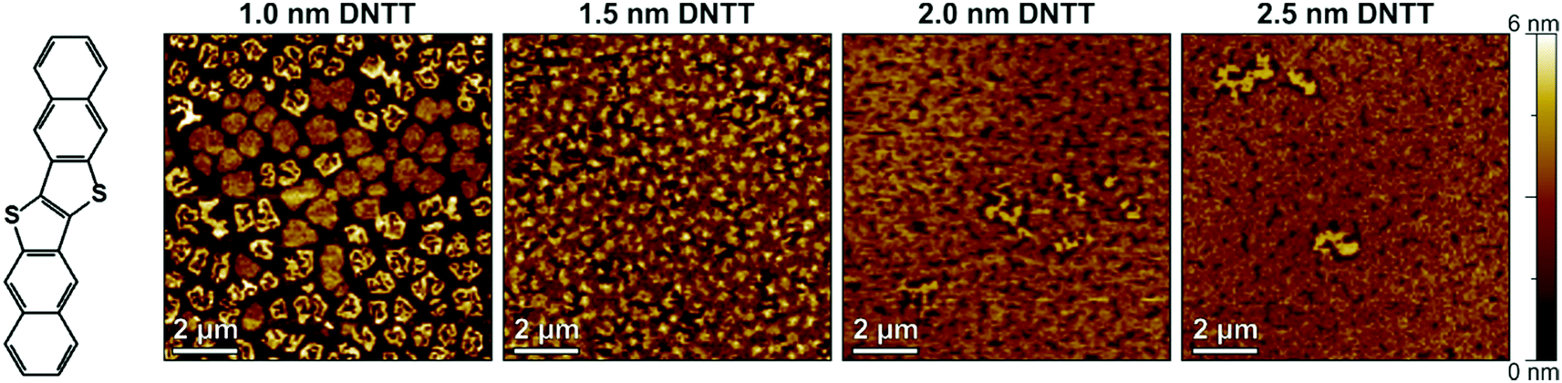 | ||
| Fig. 1 Chemical structure of DNTT and thin-film morphology of DNTT films with nominal thicknesses of 1.0, 1.5, 2.0 and 2.5 nm deposited by thermal sublimation in vacuum onto a hybrid AlOx/n-tetradecylphosphonic acid SAM dielectric, observed by AFM within 15 minutes after completion of the DNTT deposition. | ||
Based on these results, we chose 2.5 nm as the minimum nominal DNTT thickness for the experiments described below. Based on the fact that the DNTT molecules have a length of approximately 1.6 nm and stand approximately upright on the substrate surface (as confirmed by the height profile shown in Fig. S1, ESI†),31 a nominal thickness of 2.5 nm corresponds to less than two complete molecular monolayers. As the nominal DNTT thickness is increased from 1.0 to 2.5 nm, the RMS surface roughness decreases from 1.86 nm to 0.69 nm (see Table S1, ESI†), indicating a more planar and uniform film morphology with increasing nominal thickness.
Changes in the morphology of ultrathin DNTT films observed by AFM
Having determined the minimum nominal DNTT thickness required for functional TFTs to be 2.5 nm, we then monitored the time-dependent changes in the morphology of these films. For this purpose, AFM images were recorded on a nominally 2.5 nm-thick DNTT film in a quasi-continuous manner by repeatedly scanning the same area on the surface of the DNTT film over a period of 12 hours, making it possible to observe the process of the spontaneous structural reconfiguration essentially in real time. A time-lapse video is available in the ESI,† and Fig. 2 shows six snapshots obtained in intervals of three hours, with the first image taken within 15 minutes after completion of the DNTT deposition. To rule out that the morphological changes seen in these AFM images were caused by the force of the AFM tip, an identical substrate was prepared on which AFM images were taken only at 15 minutes after completion of the DNTT deposition and again at 12 hours after deposition, and these images indicate the same time-dependent changes in the morphology of the DNTT films.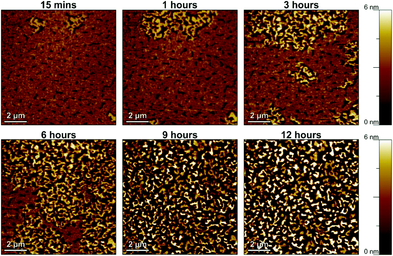 | ||
| Fig. 2 Spontaneously occurring morphological changes in a DNTT film with a nominal thickness of 2.5 nm deposited by thermal sublimation in vacuum onto a hybrid AlOx/n-tetradecylphosphonic acid SAM dielectric, observed by AFM over a period of 12 hours. A full-length video is available in the ESI,† and results for DNTT films deposited onto bare AlOx (without SAM) and onto AlOx covered with a SAM of either n-hexylphosphonic acid or n-octadecylphosphonic acid are shown in Fig. S2 (ESI†). | ||
The AFM images confirm the spontaneous rearrangement of the ultrathin DNTT films, as reported by Breuer et al.33 The maximum height of the DNTT film evolves from 3.18 nm (about 2 molecular monolayers) 15 minutes after deposition to 10.9 nm (about 6 to 7 molecular monolayers) 12 hours after deposition, while the root-mean-square surface roughness increases from 0.69 to 2.61 nm (see Table S1, ESI†). This increase in the maximum height and RMS surface roughness is accompanied by the appearance of tall, disconnected islands and by a substantial reduction of the surface coverage, i.e., by the appearance of larger and larger areas of the dielectric not covered with DNTT.
The measurements in Fig. 2 were performed on a DNTT film with a nominal thickness of 2.5 nm deposited onto an AlOx/n-tetradecylphosphonic acid SAM dielectric. Since morphological changes in ultrathin DNTT films were previously observed also on other dielectrics,33 we also performed AFM measurements on nominally 2.5 nm-thick DNTT films deposited onto bare AlOx (without SAM) and onto AlOx covered with a SAM of either n-hexylphosphonic acid or n-octadecylphosphonic acid.48 The results of these measurements are summarized in Fig. S2 (ESI†). Although there are some minor differences in the initial morphology of the ultrathin DNTT films on these surfaces, presumably due to differences in the surface energy and the packing density of the SAMs,48–51 the morphological changes in the ultrathin DNTT films are quite similar, suggesting that they are not significantly affected by the surface energy of the substrate. Results of X-ray diffraction measurements performed on DNTT films with a nominal thickness of 10 nm, summarized in Fig. S3 (ESI†), confirm that the DNTT molecules adopt an upright-standing molecular orientation.33
Influence of the changes in the DNTT thin-film morphology on the TFT characteristics
To investigate how the spontaneous morphological changes in the DNTT films described above affect the performance of TFTs in which such films serve as the semiconductor, we fabricated TFTs in the inverted coplanar (bottom-gate, bottom-contact) architecture. The TFTs were fabricated on oxidized silicon substrates to minimize the surface roughness. Aluminum gate electrodes with a root-mean-square surface roughness of less than 1 nm were deposited by thermal evaporation in vacuum.52 The gate dielectric consists of plasma-grown AlOx and an n-tetradecylphosphonic acid SAM.42 Gold source/drain contacts were deposited by thermal evaporation in vacuum and functionalized with a monolayer of pentafluorobenzenethiol (PFBT) to minimize the contact resistance.53 DNTT was deposited by vacuum sublimation with a rate of about 2 nm min−1.44 The deposition rate and the nominal thickness of the DNTT films were measured using a quartz-crystal microbalance positioned in close proximity to the substrate holder. TFTs with a nominal DNTT thickness of either 2.5 or 25 nm were fabricated. The current–voltage characteristics of the TFTs were measured on a probe station in ambient air at room temperature. The first measurement was performed within 15 minutes after the completion of the DNTT deposition, and the substrates were stored in ambient air at room temperature between measurements.The results are summarized in Fig. 3. The initial TFT characteristics are quite similar, with effective charge-carrier mobilities and threshold voltages of 0.4 cm2 V−1 s−1 and −1.5 V for a nominal DNTT thickness of 2.5 nm (Fig. 3a and Fig. S4a, ESI†) and 1 cm2 V−1 s−1 and −1.7 V for a nominal thickness of 25 nm (Fig. 3b and Fig. S4b, ESI†). This confirms that it is indeed possible to fabricate functional TFTs based on vacuum-deposited DNTT films with a nominal thickness of less than two molecular monolayers.
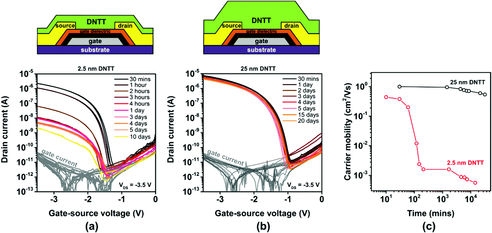 | ||
| Fig. 3 Influence of the nominal thickness of vacuum-deposited DNTT films on the evolution of the electrical characteristics of TFTs based on these films. (a) Measured transfer curves of TFTs with an ultrathin DNTT film (nominal thickness of 2.5 nm) measured repeatedly over a period of 10 days after TFT fabrication. (b) Transfer curves of TFTs with a thick DNTT film (nominal thickness of 25 nm) measured over a period of 20 days after fabrication. (c) Evolution of the effective charge-carrier mobility extracted from the measured transfer curves. All TFTs have a channel length of 20 μm and a channel width of 100 μm. | ||
However, the evolution of the effective charge-carrier mobility is dramatically different for the two nominal DNTT thicknesses. While the effective charge-carrier mobility of the TFTs with the thick DNTT film decreases by less than 20% over a period of 20 days, the effective carrier mobility of the TFTs with the ultrathin DNTT film decreases far more rapidly and far more dramatically, from initially 0.4 to 0.0007 cm2 V−1 s−1 (a 99.9% decrease) within five days (Fig. 3c). The rapid decrease of the effective carrier mobility of the TFTs with the ultrathin DNTT film seen in Fig. 3c is consistent with the rapid reduction of the surface coverage of the semiconductor and the degree of percolation through the ultrathin DNTT film during the spontaneous rearrangement of the initially closed (or at least connected) ultrathin film into disconnected islands seen in Fig. 2. Although the morphological changes commence immediately after the completion of the DNTT deposition, their cumulative impact on the surface coverage and the degree of percolation appears to be most pronounced during the period between about one hour and about six hours after the DNTT deposition, which explains the observation that the drop in the effective charge-carrier mobility is most prominent during this period. The results confirm the severe impact of the spontaneous morphological changes of ultrathin DNTT films reported by Breuer et al.33 on the effective charge-transport characteristics.
The thick DNTT films are far more stable than the ultrathin DNTT films, both in terms of the film morphology as observed by AFM (see Fig. S5, ESI†) and in terms of the electrical TFT characteristics (see Fig. 3b). This was already reported by Breuer et al.33 and indicates that the spontaneous disaggregation of the first molecular monolayer into disconnected islands seen in Fig. 2 is effectively prevented when this first molecular monolayer is covered with a sufficient amount of additional material.
Effect of cryogenic cooling of ultrathin DNTT films
To confirm that the spontaneously occurring mass transport within the ultrathin DNTT films that leads to the disaggregation of the initially closed monolayer is indeed thermally activated, we cooled a substrate with an ultrathin DNTT film to a temperature of 193 K in dry nitrogen immediately after completion of the DNTT deposition and stored it at this temperature for a duration of 18 days. After allowing the substrate to warm up to room temperature, we immediately recorded an AFM image. An identical substrate with an identical ultrathin DNTT film served as a reference on which an AFM image was recorded immediately after the DNTT deposition and which was kept in ambient air at room temperature for a period of two weeks, after which another AFM image was taken. The results are summarized in Fig. 4.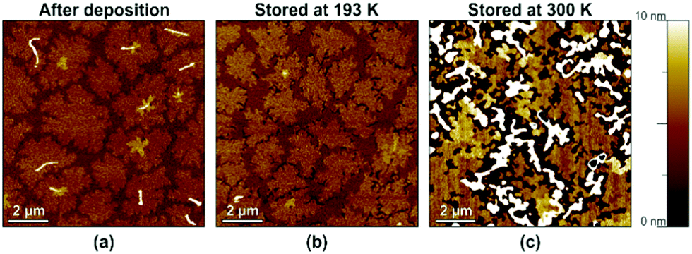 | ||
| Fig. 4 Effect of cryogenic cooling on the spontaneously occurring morphological changes in ultrathin DNTT films, observed by AFM at room temperature. (a) DNTT morphology immediately after completion of the DNTT deposition. (b) DNTT morphology after the substrate had been stored at a temperature of 193 K for 18 days. (c) DNTT morphology on a reference substrate stored at room temperature for two weeks. | ||
Fig. 4a shows the AFM image recorded immediately after the DNTT deposition, indicating the initial closed-monolayer morphology (with a second monolayer seen as yet-disconnected islands). Fig. 4b confirms that this closed-monolayer morphology is perfectly preserved during storage at cryogenic temperature for 18 days. For comparison, Fig. 4c shows the break-up of the initially closed DNTT monolayer into tall, disconnected islands observed on the reference substrate after it had been stored at room temperature for two weeks (and also observed on the substrate that had been stored at cryogenic temperature within less than a day after it had been returned to room temperature). These observations strongly support the hypothesis that these morphological changes in the ultrathin DNTT films are indeed thermally activated.35
In situ encapsulation of ultrathin DNTT films
As discussed in the Introduction, the morphological changes in the ultrathin DNTT films proceed by lateral and vertical mass transport that causes a rearrangement of the initially closed (or at least connected) single-monolayer-thick films into disconnected islands. While the results in Fig. 4 confirm that this mass transport is indeed thermally activated, the results in Fig. 3b show that it can be prevented by covering the ultrathin films with additional material (in the case of Fig. 3b with additional DNTT). In the following we explore the extent to which this can also be accomplished using other encapsulation materials. Our choice of these materials was dictated by the requirement to deposit the encapsulation immediately (within one to two minutes) following the completion of the deposition of the ultrathin DNTT film in the same vacuum-deposition system and without breaking the vacuum. This ruled out virtually all popular organic-TFT-encapsulation materials, such as Al2O3,45 Cytop46 and parylene,47 as none of these can be deposited in the vacuum-deposition system in which the DNTT films are deposited. The three materials we selected for the in situ encapsulation of ultrathin DNTT films are polytetrafluoroethylene (PTFE), C60 and titanyl phthalocyanine (TiOPc).Encapsulation using vacuum-deposited polytetrafluoroethylene (PTFE)
Polytetrafluoroethylene (PTFE) is a synthetic fluoropolymer available as a powder that can be deposited by thermal sublimation in vacuum. PTFE is an excellent electrical insulator and has been used previously to encapsulate pentacene TFTs.54 We deposited PTFE films with a nominal thickness of either 2.5 or 10 nm directly onto ultrathin DNTT films having a nominal thickness of 2.5 nm. The PTFE deposition was started within one to two minutes after completion of the DNTT deposition in the same vacuum-deposition system without breaking vacuum, by using one sublimation source for the DNTT deposition and another for the PTFE deposition. AFM images of a nominally 2.5 nm-thick PTFE film deposited onto a nominally 2.5 nm-thick DNTT film recorded within 15 minutes after the completion of the PTFE deposition and again after 72 hours are shown in Fig. S6b (ESI†). The AFM images indicate the occurrence of time-dependent morphological changes, but since it is not possible to distinguish the two materials in the AFM images, it is difficult to draw any useful conclusions from the images alone.The results of the TFT measurements are summarized in Fig. 5. As can be seen, the initial TFT characteristics are not significantly affected by the PTFE encapsulation, but the degradation of the charge-carrier mobility is notably decelerated by the PTFE encapsulation, especially for the larger PTFE thickness (10 nm). However, even with the nominally 10 nm-thick PTFE encapsulation, the charge-carrier mobility of the TFTs still decreases by approximately one order of magnitude (from 0.8 to 0.08 cm2 V−1 s−1) within two months. Analysis of thin PTFE films deposited onto other surfaces suggests that PTFE films also undergo morphological changes (as seen in Fig. S7 and S8, ESI†),55,56 and assuming these changes also occur in PTFE films deposited onto DNTT, this might explain the limited effectiveness of the PTFE encapsulation observed here. Nevertheless, as it is apparent that increasing the PTFE thickness from 2.5 to 10 nm increases the encapsulation effectiveness, we attempted the deposition of PTFE encapsulations with a nominal thickness of more than 10 nm, but this turned out to be quite challenging and prohibitively time-consuming in our deposition system, due to the unfavorable combination of the high vapor pressure of the PTFE powder and the limited throughput of the vacuum pump.
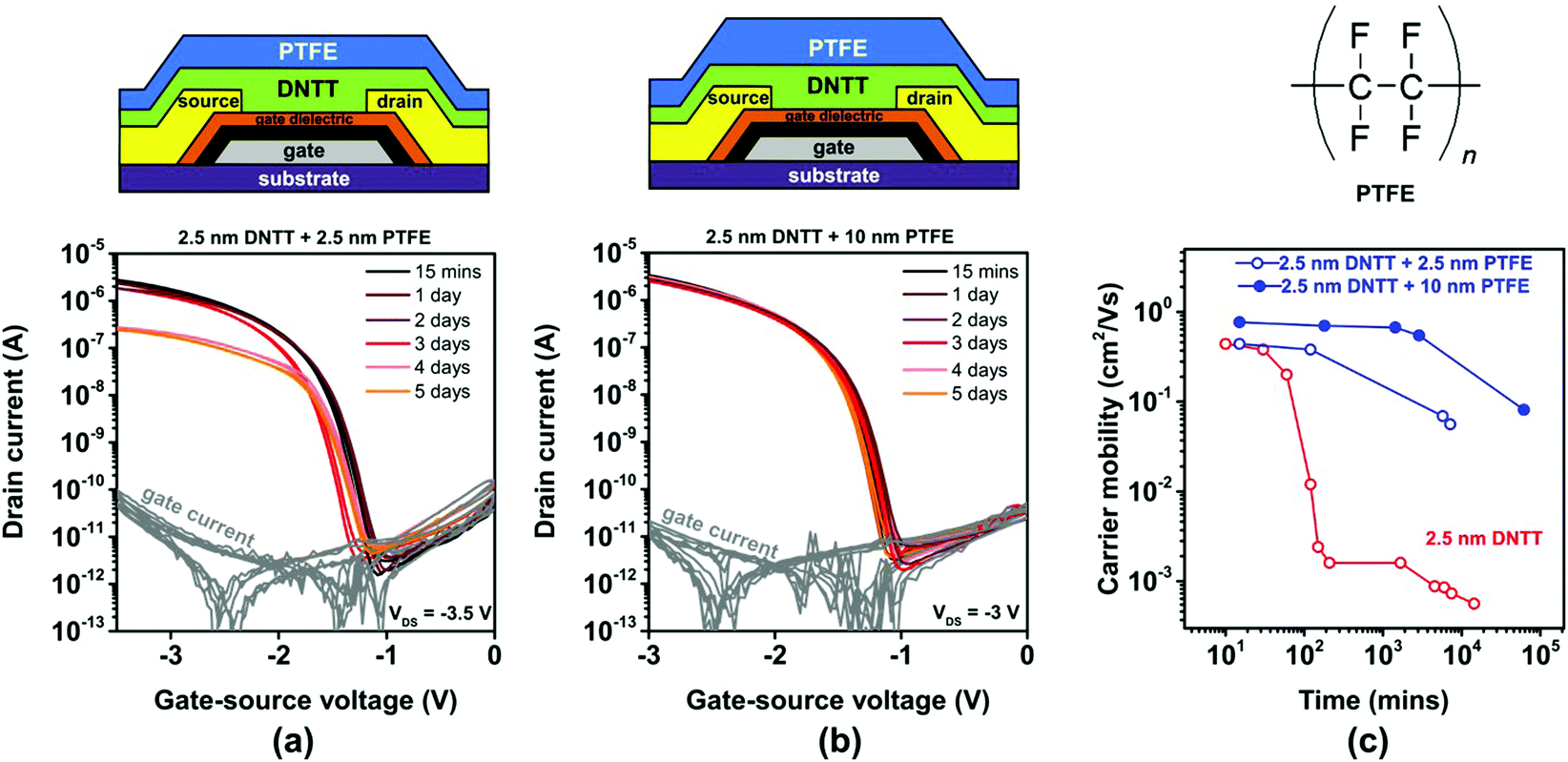 | ||
| Fig. 5 Effect of in situ encapsulation of ultrathin, vacuum-deposited DNTT films (having a nominal thickness of 2.5 nm) with vacuum-deposited PTFE on the evolution of the TFT characteristics. Transfer curves of TFTs encapsulated with a nominally (a) 2.5 nm-thick and (b) 10 nm-thick PTFE film, measured repeatedly over a period of 5 days after TFT fabrication. (c) Evolution of the effective charge-carrier mobility extracted from the measured transfer curves. | ||
Encapsulation using vacuum-deposited C60
As an alternative to PTFE, we tested C60 for the encapsulation of ultrathin DNTT films. The vapor pressure of C60 is substantially smaller than that of PTFE, so that thick C60 films can be easily deposited by sublimation in vacuum. Other potential benefits of C60 for the purpose of encapsulating ultrathin DNTT films are the superior thermal and mechanical stability of C60 films57 and the fact that C60 does not form undesirable Diels–Alder adducts with DNTT.58 A substantial drawback of C60 for this purpose is the fact that it is an electron-transporting semiconductor and thus expected to adversely affect the current–voltage characteristics of the DNTT TFTs, especially their off-state behavior, due to the uncontrollable flow of electrons from the drain contact through the C60 film to the source contact. We deposited C60 films with a nominal thickness of either 2.5 or 25 nm directly onto ultrathin DNTT films having a nominal thickness of 2.5 nm.The results are summarized in Fig. 6. As can be seen in Fig. 6b, the deposition of a nominally 25 nm-thick film of C60 indeed causes ambipolar transistor behavior, which is highly undesirable, as it increases the off-state leakage current of the TFTs and thus the static power consumption and the noise margins of logic circuits based on ambipolar TFTs. However, the degradation of the hole mobility in the ultrathin DNTT film is notably decelerated by the C60 encapsulation, which suggests that the morphology of the ultrathin DNTT film is indeed greatly stabilized by the C60 encapsulation.
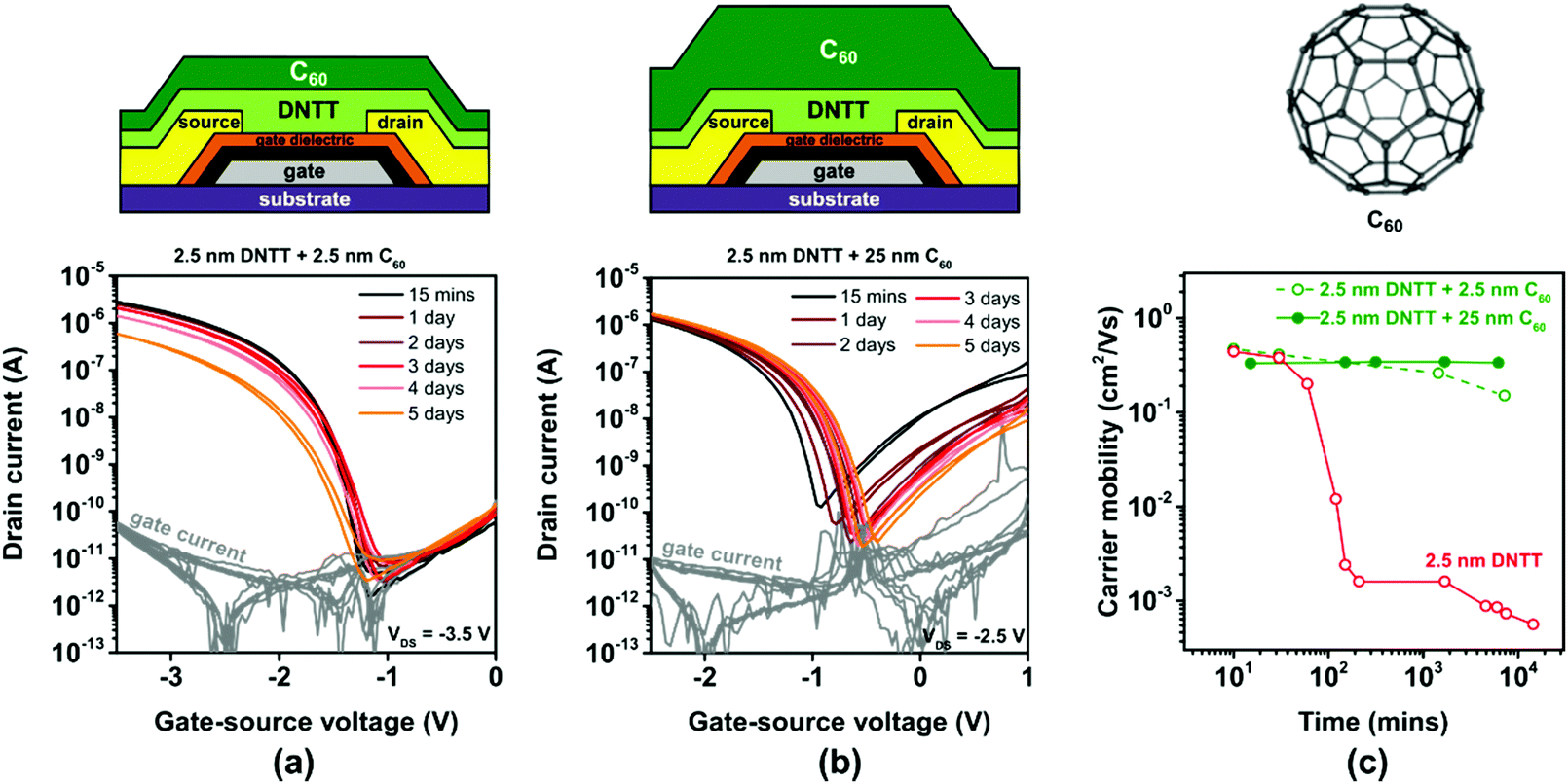 | ||
| Fig. 6 Effect of in situ encapsulation of ultrathin, vacuum-deposited DNTT films (having a nominal thickness of 2.5 nm) with vacuum-deposited C60 on the evolution of the TFT characteristics. Transfer curves of TFTs encapsulated with a nominally (a) 2.5 nm-thick and (b) 25 nm-thick C60 film, measured repeatedly over a period of 5 days after TFT fabrication. (c) Evolution of the effective charge-carrier mobility extracted from the measured transfer curves. | ||
A workable compromise between the beneficial effect of stabilizing the morphology of the ultrathin DNTT films and the drawback of increasing the leakage current is the use of a C60 encapsulation with a smaller thickness, as shown in Fig. 6a. With a nominally 2.5 nm-thick C60 encapsulation, the off-state drain current of the ultrathin-DNTT TFTs is approximately 10−10 A, which is similar to that of ultrathin-DNTT TFTs without encapsulation (Fig. 3a) or with an electrically insulating encapsulation (Fig. 5a). However, the suppression of the degradation of the hole mobility in the ultrathin DNTT film is not quite as pronounced as in the case of the nominally 25 nm-thick C60 encapsulation (Fig. 6c). This is mainly due to the fact that the deposition of nominally 2.5 nm-thick C60 does not lead to the formation of a closed C60 film on the surface of the ultrathin DNTT film, but rather to edge decoration, as seen in Fig. S6c (ESI†) (and as reported previously for C60 deposited onto pentacene59).
Encapsulation using vacuum-deposited titanyl phthalocyanine (TiOPc)
TiOPc is a hole-transporting small-molecule semiconductor.60 TiOPc molecules usually adopt a flat-lying orientation when deposited onto metals,61 but an upright-standing molecular orientation when deposited onto electrically insulating surfaces or organic-semiconductor films.62 A potential benefit of TiOPc for the purpose of encapsulating ultrathin DNTT films is its excellent chemical robustness and thermal stability. A drawback of TiOPc for this purpose is that we cannot rule out that the TiOPc film will transport a hole current in parallel to the ultrathin DNTT film, thus making it impossible to monitor the electrical behavior of the DNTT film exclusively. We deposited TiOPc films with a nominal thickness of either 2.5 or 25 nm directly onto ultrathin DNTT films.The results are summarized in Fig. 7. The first observation is that the current–voltage characteristics of the ultrathin-DNTT TFTs with the TiOPc encapsulation (Fig. 7a and b) are exactly the same as those of the ultrathin-DNTT TFTs without encapsulation (Fig. 3a). This suggests that the TiOPc film does not participate in the charge transport, which is in contradiction to the results reported previously for TFTs based on a heterostructure of ultrathin dihexyl-sexithiophene and TiOPc, but this may be due to the fact that the carrier mobility in DNTT is significantly larger than that in both TiOPc and dihexyl-sexithiophene.
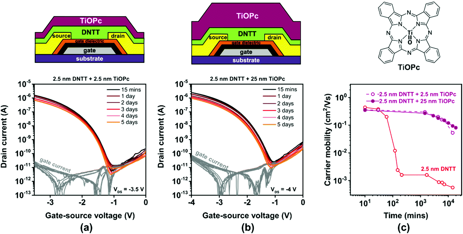 | ||
| Fig. 7 Effect of in situ encapsulation of ultrathin, vacuum-deposited DNTT films (having a nominal thickness of 2.5 nm) with vacuum-deposited TiOPc on the evolution of the TFT characteristics. Transfer curves of TFTs encapsulated with a nominally (a) 2.5 nm-thick and (b) 25 nm-thick TiOPc film, measured repeatedly over a period of 5 days after TFT fabrication. (c) Evolution of the effective charge-carrier mobility extracted from the measured transfer curves. | ||
The second observation is that the TiOPc encapsulation slows down the degradation of the charge-carrier mobility of the TFTs, similar to encapsulation with PTFE and C60. However, in stark contrast to PTFE (Fig. 5) and C60 (Fig. 6), this effect is virtually independent of the thickness of the TiOPc encapsulation. Nevertheless, the charge-carrier mobility of the TiOPc-encapsulated TFTs still decreases by approximately one order of magnitude within two weeks.
Summary of encapsulation results
The results from the encapsulation experiments are summarized in Fig. 8. The transfer curves of the TFTs with and without the various encapsulation films recorded within 30 minutes after the last deposition and the evolution of the subthreshold swings extracted from these transfer curves are summarized in Fig. S9 (ESI†). The TFTs with the thick DNTT films (nominal thickness 25 nm) initially have an effective carrier mobility of 1 cm2 V−1 s−1 (Fig. 8a), which is similar to previous reports of bottom-gate, bottom contact DNTT TFTs.13 The effective mobility of these TFTs degrades from 1 to 0.8 cm2 V−1 s−1 within 5 days and to 0.5 cm2 V−1 s−1 within 23 days (see also Fig. 3c). This degradation in effective mobility is notably more rapid than the mobility degradation in top-contact DNTT TFTs,63 but for the experiments described here, it was necessary to fabricate the TFTs in the bottom-contact architecture in order to minimize the delay between the completion of the DNTT deposition and the first measurement of the current–voltage characteristics. The long-term stability of bottom-contact DNTT TFTs has to our knowledge not been previously reported, and the reasons for the relatively rapid degradation of the effective mobility observed here is not known, but it may be related to a degradation of the interface between the source/drain contacts and the vacuum-deposited DNTT film.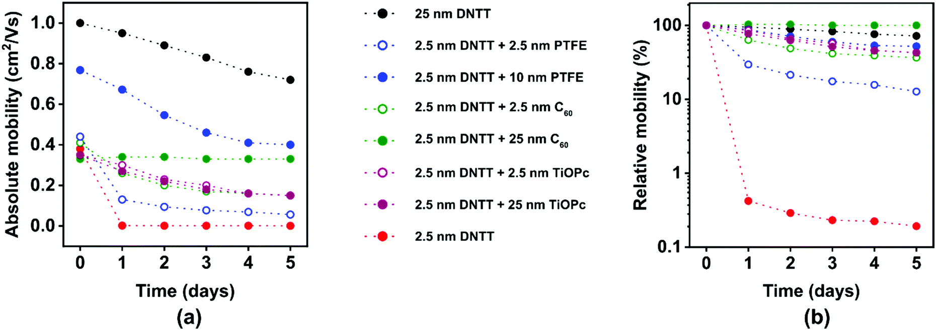 | ||
| Fig. 8 Evolution of the effective charge-carrier mobilities of TFTs based on vacuum-deposited DNTT films with nominal thicknesses of 2.5 and 25 nm with and without encapsulation with PTFE, C60 or TiOPc with various nominal thicknesses. (a) Absolute value of the effective carrier mobility. (b) Effective carrier mobility normalized to the mobility measured immediately after TFT fabrication. | ||
The TFTs with the ultrathin DNTT films (nominal thickness 2.5 nm) initially have effective carrier mobilities between 0.3 and 0.4 cm2 V−1 s−1, regardless of whether they were encapsulated or not and, if so, regardless of the encapsulation material (PTFE, C60, TiOPc) and the nominal thickness of the encapsulation film (Fig. 8a). The only exception is the TFT in which the ultrathin DNTT film was encapsulated with a nominally 10 nm-thick PTFE film, which has a somewhat larger initial mobility (0.7 cm2 V−1 s−1). The reason for this discrepancy is unknown, but it may be the result of unavoidable substrate-to-substrate variations in the fabrication process. The results confirm that it is indeed possible to fabricate functional TFTs based on vacuum-deposited DNTT films with a nominal thickness of less than two molecular monolayers.
Encapsulation of these films has a pronounced effect on their stability: while the effective mobility of unencapsulated ultrathin DNTT films decreases by two orders of magnitude within a day, the mobility of encapsulated films decreases by less than one order of magnitude within five days (Fig. 8b). The mechanism by which the encapsulation of the ultrathin DNTT films decelerates the degradation of the carrier mobility in these films is not by protecting the DNTT molecules from ambient air (given the outstanding chemical stability of DNTT during long-term exposure to air and humidity24), but by stabilizing the fragile morphology of the ultrathin DNTT films by burying it under a thick film of additional mass. Although we are unable to inspect the morphology of the aged ultrathin DNTT films buried underneath the thick encapsulation films by AFM measurements, we hypothesize that the deceleration of the mobility degradation observed here is a direct result of preventing mass transport within the ultrathin DNTT films by the encapsulation film. This hypothesis is supported by the observation that for two of the three encapsulation materials, thicker encapsulation films provide better stability (Fig. 8b). The interesting question for how long the encapsulation can delay the break-up of the initially closed DNTT monolayer is beyond the scope of the present study.
The choice of the encapsulation material is dictated by a number of considerations. Since the spontaneous structural reconfiguration of the ultrathin DNTT films commences immediately after the DNTT deposition, it is necessary to start the deposition of the encapsulation film immediately after the completion of the DNTT deposition. This limits the choice of encapsulation materials to such materials that can be deposited in the same high-vacuum system in which the ultrathin DNTT films are deposited, without breaking vacuum and without time-consuming substrate transfers. If the purpose of the experiments is an investigation of the charge transport in ultrathin DNTT films, the choice of encapsulation materials should be limited to materials that do not participate in the charge transport. Of the three materials we have tested here, this obviously eliminates C60 (and possibly also TiOPc, although Fig. 7 seems to indicate that the TiOPc films do not participate in charge transport). The observation that the stabilizing effect of the encapsulation increases with increasing thickness of the encapsulation film calls for materials that can be easily deposited as thick films. Unfortunately, this essentially eliminates PTFE, due to its unfavorably high vapor pressure.
Another aspect to be considered in the choice of the encapsulation material is the homogeneity and long-term morphological stability of the encapsulation film, which would likely benefit from choosing materials with a higher molecular weight and thus smaller diffusivity on the DNTT surface, and possibly also from performing the deposition of the encapsulation film at cryogenic temperatures to promote homogeneous coverage of the encapsulating material.59
Conclusions
We have monitored the spontaneously occurring changes in the thin-film morphology of vacuum-deposited ultrathin DNTT films by AFM and analyzed how this spontaneous structural reconfiguration affects the electric characteristics of TFTs based on such films. Our results confirm that the observed transition from an initially closed (or at least connected) monolayer to tall, isolated islands and the associated loss of percolation through the films cause a rapid and substantial degradation of the effective charge-carrier mobility of the TFTs. By showing that these morphological changes are prevented by keeping the substrates at cryogenic temperatures, we have confirmed that this structural reorganization is indeed thermally activated. We have also tested the extent to which encapsulation using three different materials, PTFE, C60, and TiOPc, is able to stabilize the morphology of the ultrathin DNTT films. Although we have not been able to stop the morphological changes entirely, we have found that encapsulation can slow the rate of degradation quite significantly. The ability to fabricate TFTs based on vacuum-deposited ultrathin organic–semiconductor films with sufficient long-term stability is potentially of interest for interface and charge-transport investigations.Experimental section
Film characterization
Samples for film characterization were prepared on silicon substrates. Silicon was chosen as the substrate to provide the smallest possible surface roughness. Aluminum with a thickness of 30 nm and a root-mean-square surface roughness of less than 1 nm was deposited by thermal evaporation in vacuum at a rate of 2 nm s−1.52 The aluminum surface was exposed to an RF oxygen plasma (oxygen flow rate: 30 sccm, oxygen partial pressure: 10 mTorr, RF power: 200 W, duration: 30 s) to increase the thickness of the native aluminum oxide (AlOx) to about 3.6 nm. On some substrates, ultrathin DNTT (Sigma-Aldrich) was deposited directly onto bare AlOx. On other substrates, a monolayer of n-tetradecylphosphonic acid, n-hexylphosphonic acid, or n-octadecylphosphonic acid (PCI Synthesis, Newburyport, MA, USA) was allowed to self-assemble on the AlOx surface by immersing the substrates into a 1 mM-solution of the phosphonic acid in 2-proponal for a duration of 12 hours, after which the substrates were rinsed with 2-proponal, dried with nitrogen and heated to a temperature of 80 °C for 10 minutes to stabilize the monolayer.64 DNTT was deposited by thermal sublimation in vacuum at a rate of 2 nm min−1 (without heating the substrate to avoid the unnecessary acceleration of the morphological changes). AFM images were acquired in tapping mode using a Bruker Nanoscope III MultiMode® or an Agilent SPM 5500 and cantilevers with resonance frequencies between 200 and 500 kHz and a typical tip radius of 8 nm. X-ray diffraction measurements were performed using a Bruker D8 Discovery diffractometer with monochromatized Cu Kα radiation (λ = 1.542 Å) and a sensitive one-dimensional LynxEye silicon strip detector. All AFM and XRD measurements were performed in ambient air at room temperature.TFT fabrication and characterization
TFTs were fabricated in the inverted coplanar (bottom-gate, bottom-contact) architecture on silicon substrates coated with 100 nm-thick thermally grown silicon dioxide. This device architecture was chosen to minimize the delay between the completion of the semiconductor deposition and the first measurement of the current–voltage characteristics. Aluminum gate electrodes with a thickness of 30 nm were deposited by thermal evaporation in vacuum at a rate of 2 nm s−1. The gate dielectric consists of a thin, oxygen-plasma-grown film of AlOx and a solution-processed n-tetradecylphosphonic acid SAM and has a capacitance of about 0.7 μF cm−2.42 For the source and drain contacts, titanium with a thickness of 0.2 nm (to improve adhesion) and gold with a thickness of 30 nm were sequentially deposited by thermal evaporation in vacuum. To minimize the contact resistance, the surface of the Au source/drain contacts was functionalized with a monolayer of pentafluorobenzenethiol (PFBT).53 DNTT was deposited by thermal sublimation in vacuum (base pressure 10−6 mbar; substrate temperature 20 °C) at a rate of 2 nm min−1. PTFE (Sigma-Aldrich, free-flowing powder, particle size <12 μm), C60 (Sigma-Aldrich) or TiOPc (Sigma-Aldrich) encapsulation films were deposited by thermal sublimation in vacuum within one to two minutes after completion of the DNTT deposition. Deposition rate and nominal thickness of all vacuum-deposited films were measured using a quartz-crystal microbalance positioned in close proximity to the substrate holder. Gate electrodes, source/drain contacts, organic semiconductor and encapsulation films were all patterned using polyimide shadow masks (CADiLAC Laser, Hilpoltstein, Germany). The TFTs have a channel length of 20 μm and a channel width of 100 μm. The electrical measurements were performed in ambient air at room temperature using a manual probe station and an Agilent 4156C Semiconductor Parameter Analyzer. The first measurement was performed within 15 minutes after the completion of the last vacuum deposition, and the substrates were stored in ambient air at room temperature between measurements.Conflicts of interest
There are no conflicts to declare.Acknowledgements
This work is partially funded by the German Research Foundation (DFG) under the Grants No. K. L. 2223/6-2 (SPP FFlexCom), K. L. 2223/7-1, INST 35/1429-1 (SFB 1249) and 223848855-SFB 1083 (TP A2). D. G. gratefully acknowledges financial support by the Cusanuswerk. Open Access funding provided by the Max Planck Society.Notes and references
- M. Noda, N. Kobayashi, M. Katsuhara, A. Yumoto, S. Ushikura, R. Yasuda, N. Hirai, G. Yukawa, I. Yagi, K. Nomoto and T. Urabe, J. Soc. Inf. Disp., 2011, 19, 316–322 CrossRef CAS.
- B. Peng, X. Ren, Z. Wang, X. Wang, R. C. Roberts and P. K. L. Chan, Sci. Rep., 2014, 4, 6430 CrossRef CAS.
- H. Fuketa, K. Yoshioka, Y. Shinozuka and K. Ishida, IEEE Trans. Biomed. Eng., 2014, 8, 824–833 Search PubMed.
- Y. Chu, X. Wu, J. Lu, D. Liu, J. Du, G. Zhang and J. Huang, Adv. Sci., 2016, 3, 1500435 CrossRef.
- M. Kaltenbrunner, T. Sekitani, J. Reeder, T. Yokota, K. Kuribara, T. Tokuhara, M. Drack, R. Schwödiauer, I. Graz, S. Bauer-Gogonea, S. Bauer and T. Someya, Nature, 2013, 499, 458–463 CrossRef CAS.
- S. Lee, A. Reuveny, J. Reeder, S. Lee, H. Jin, Q. Liu, T. Yokota, T. Sekitani, T. Isoyama, Y. Abe, Z. Suo and T. Someya, Nat. Nanotechnol., 2016, 11, 472–478 CrossRef CAS.
- W. Lee, D. Kim, J. Rivnay, N. Matsuhisa, T. Lonjaret, T. Yokota, H. Yawo, M. Sekino, G. G. Malliaras and T. Someya, Adv. Mater., 2016, 28, 9722–9728 CrossRef CAS.
- X. Ren, K. Pei, B. Peng, Z. Zhang, Z. Wang, X. Wang and P. K. L. Chan, Adv. Mater., 2016, 28, 4832–4838 CrossRef CAS.
- M. Kondo, M. Melzer, D. Karnaushenko, T. Uemura, S. Yoshimoto and M. Akiyama, Sci. Adv., 2020, 6, eaay6094 CrossRef CAS.
- F. Dinelli, M. Murgia, P. Levy, M. Cavallini, F. Biscarini and D. M. De Leeuw, Phys. Rev. Lett., 2004, 92, 90–93 CrossRef.
- F. J. Zhang, C. A. Di, N. Berdunov, Y. Hu, Y. Hu, X. Gao, Q. Meng, H. Sirringhaus and D. Zhu, Adv. Mater., 2013, 25, 1401–1407 CrossRef CAS.
- T. Someya, A. Dodabalapur, J. Huang, K. C. See and H. E. Katz, Adv. Mater., 2010, 22, 3799–3811 CrossRef CAS.
- Y. Fujisaki, Y. Nakajima, T. Takei, H. Fukagawa, T. Yamamoto and H. Fujikake, IEEE Trans. Electron Devices, 2012, 59, 3442–3449 CAS.
- K. Fukuda, T. Sekitani, U. Zschieschang, H. Klauk, K. Kuribara, T. Yokota, T. Sugino, K. Asaka, M. Ikeda, H. Kuwabara, T. Yamamoto, K. Takimiya, T. Fukushima, T. Aida, M. Takamiya, T. Sakurai and T. Someya, Adv. Funct. Mater., 2011, 21, 4019–4027 CrossRef CAS.
- J. Milvich, T. Zaki, M. Aghamohammadi, R. Rödel, U. Kraft, H. Klauk and J. N. Burghartz, Org. Electron., 2015, 20, 63–68 CrossRef CAS.
- S. Kim, H. Moon, H. Kwon, G. Lee, D. Yu, J. Choi, J. Park, S. J. Kim and S. Yoo, Adv. Mater. Technol., 2019, 4, 1800332 CrossRef.
- K. Ishida, T. C. Huang, K. Honda, Y. Shinozuka, H. Fuketa, T. Yokota, U. Zschieschang, H. Klauk, G. Tortissier, T. Sekitani, H. Toshiyoshi, M. Takamiya, T. Someya and T. Sakurai, IEEE J. Solid-State Circuits, 2013, 48, 255–264 Search PubMed.
- T. Sekitani, T. Yokota, K. Kuribara, M. Kaltenbrunner, T. Fukushima, Y. Inoue, M. Sekino, T. Isoyama, Y. Abe, H. Onodera and T. Someya, Nat. Commun., 2016, 7, 11425 CrossRef CAS.
- A. K. M. Mahfuzul Islam, M. Hamamatsu, T. Yokota, S. Lee, W. Yukita, M. Takamiya, T. Someya and T. Sakurai, IEEE J. Emerg. Sel. Top. Circuits Syst., 2017, 7, 81–91 Search PubMed.
- M. Elsobky, Y. Mahsereci, Z. Yu, H. Richter, J. N. Burghartz, J. Keck, H. Klauk and U. Zschieschang, Electron. Lett., 2018, 54, 338–340 CrossRef CAS.
- X. Zhao, H. Li, Q. Tang, Y. Tong and Y. Liu, J. Mater. Chem. C, 2019, 7, 3199–3205 RSC.
- U. Kraft, K. Takimiya, M. J. Kang, R. Rödel, F. Letzkus, J. N. Burghartz, E. Weber and H. Klauk, Org. Electronics, 2016, 35, 33–40 CrossRef CAS.
- E. D. Głowacki, S. Bauer, M. S. White, U. Monkowius, N. S. Sariciftci, M. Kaltenbrunner, L. Torsi, P. Mastrorilli, J. Gsiorowski, G. P. Suranna, T. Sekitani, G. Romanazzi, T. Someya and M. Irimia-Vladu, Adv. Mater., 2013, 25, 1563–1569 CrossRef.
- U. Zschieschang, F. Ante, D. Kälblein, T. Yamamoto, K. Takimiya, H. Kuwabara, M. Ikeda, T. Sekitani, T. Someya, J. B. Nimoth and H. Klauk, Org. Electronics, 2011, 12, 1370–1375 CrossRef CAS.
- Z. Ding, G. Abbas, H. E. Assender, J. J. Morrison, S. G. Yeates, E. R. Patchett and D. M. Taylor, ACS Appl. Mater. Interfaces, 2014, 6, 15224–15231 CrossRef CAS.
- S. Yogev, R. Matsubara, M. Nakamura, U. Zschieschang, H. Klauk and Y. Rosenwaks, Phys. Rev. Lett., 2013, 110, 036803 CrossRef CAS.
- H. S. Lee, D. H. Kim, J. H. Cho, M. Hwang, Y. Jang, K. Cho, H. S. Lee, D. H. Kim, J. H. Cho, M. Hwang and Y. Jang, J. Am. Chem. Soc., 2008, 130, 10556–10564 CrossRef CAS.
- J. A. Venables, G. D. T. Spiller and M. Hanbucken, Rep. Prog. Phys., 1984, 47, 399–459 CrossRef.
- M. C. Jung, M. R. Leyden, G. O. Nikiforov, M. V. Lee, H. K. Lee, T. J. Shin, K. Takimiya and Y. Qi, ACS Appl. Mater. Interfaces, 2015, 7, 1833–1840 CrossRef CAS.
- R. Ruiz, D. Choudhary, B. Nickel, T. Toccoli, K. C. Chang, A. C. Mayer, P. Clancy, J. M. Blakely, R. L. Headrick, S. Iannotta and G. G. Malliaras, Chem. Mater., 2004, 16, 4497–4508 CrossRef CAS.
- T. Yamamoto and K. Takimiya, J. Am. Chem. Soc., 2007, 129, 2224–2225 CrossRef CAS.
- W. Xie, K. Willa, Y. Wu, R. Häusermann, K. Takimiya, B. Batlogg and C. D. Frisbie, Adv. Mater., 2013, 25, 3478–3484 CrossRef CAS.
- T. Breuer, A. Karthäuser, H. Klemm, F. Genuzio, G. Peschel, A. Fuhrich, T. Schmidt and G. Witte, ACS Appl. Mater. Interfaces, 2017, 9, 8384–8392 CrossRef CAS.
- S. Herminghaus, K. Jacobs, K. Mecke, J. Bischof, A. Fery, M. Ibn-Elhaj and S. Schlagowski, Science, 1998, 282, 916–919 CrossRef.
- S. Rath and H. Port, Chem. Phys. Lett., 2006, 421, 152–156 CrossRef CAS.
- A. C. Dürr, F. Schreiber, K. A. Ritley, V. Kruppa, J. Krug, H. Dosch and B. Struth, Phys. Rev. Lett., 2003, 90, 016104 CrossRef.
- D. Käfer, C. Wöll and G. Witte, Appl. Phys. A: Mater. Sci. Process., 2009, 95, 273–284 CrossRef.
- A. Amassian, V. A. Pozdin, T. V. Desai, S. Hong, A. R. Woll, J. D. Ferguson, J. D. Brock, G. G. Malliaras and J. R. Engstrom, J. Mater. Chem., 2009, 19, 5580–5592 RSC.
- A. A. Virkar, S. Mannsfeld, Z. Bao and N. Stingelin, Adv. Mater., 2010, 22, 3857–3875 CrossRef CAS.
- H. Chen, M. Li, Z. Lu, X. Wang, J. Yang, Z. Wang, F. Zhang, C. Gu, W. Zhang, Y. Sun, J. Sun, W. Zhu and X. Guo, Nat. Commun., 2019, 10, 3872 CrossRef.
- S. Lee, Y. Inoue, D. Kim, A. Reuveny, K. Kuribara, T. Yokota, J. Reeder, M. Sekino, T. Sekitani, Y. Abe and T. Someya, Nat. Commun., 2014, 5, 5898 CrossRef CAS.
- U. Zschieschang and H. Klauk, Org. Electronics, 2015, 25, 340–344 CrossRef CAS.
- U. Kraft, T. Zaki, F. Letzkus, J. N. Burghartz, E. Weber, B. Murmann and H. Klauk, Adv. Electron. Mater., 2019, 5, 1800453 CrossRef.
- R. Acharya, B. Peng, P. K. L. Chan, G. Schmitz and H. Klauk, ACS Appl. Mater. Interfaces, 2019, 11, 27104–27111 CrossRef CAS.
- D. Yu, Y. Q. Yang, Z. Chen, Y. Tao and Y. F. Liu, Opt. Commun., 2016, 362, 43–49 CrossRef CAS.
- J. M. Kim, J. Oh, K. M. Jung, K. C. Park, J. H. Jeon and Y. S. Kim, Semicond. Sci. Technol., 2019, 34, 075015 CrossRef CAS.
- D. Feili, M. Schuettler, T. Doerge, S. Kammer and T. Stieglitz, Sens. Actuators, A, 2005, 120, 101–109 CrossRef CAS.
- O. Acton, G. G. Ting, P. J. Shamberger, F. S. Ohuchi, H. Ma and A. K. Y. Jen, ACS Appl. Mater. Interfaces, 2010, 2, 511–520 CrossRef CAS.
- K. Fukuda, T. Hamamoto, T. Yokota, T. Sekitani, U. Zschieschang, H. Klauk and T. Someya, Appl. Phys. Lett., 2009, 95, 203301 CrossRef.
- A. Jedaa, M. Burkhardt, U. Zschieschang, H. Klauk, D. Habich, G. Schmid and M. Halik, Org. Electronics, 2009, 10, 1442–1447 CrossRef CAS.
- D. M. Spori, N. V. Venkataraman, S. G. P. Tosatti, F. Durmaz, N. D. Spencer and S. Zürcher, Langmuir, 2007, 23, 8053–8060 CrossRef CAS.
- M. Geiger, R. Acharya, E. Reutter, T. Ferschke, U. Zschieschang, J. Weis, J. Pflaum, H. Klauk and R. T. Weitz, Adv. Mater. Interfaces, 2020, 7, 1902145 CrossRef CAS.
- J. W. Borchert, B. Peng, F. Letzkus, J. N. Burghartz, P. K. L. Chan, K. Zojer, S. Ludwigs and H. Klauk, Nat. Commun., 2019, 10, 1119 CrossRef.
- C. Pannemann, T. Diekmann, U. Hilleringmann, U. Schürmann, M. Scharnberg, V. Zaporojtchenko, R. Adelung and F. Faupel, Mater. Sci. Pol., 2007, 25, 95–101 CAS.
- J. Fresnais, L. Benyahia and F. Poncin-Epaillard, Surf. Interface Anal., 2006, 38, 144–149 CrossRef CAS.
- N. Selway, V. Chan and J. R. Stokes, Soft Matter, 2017, 13, 1702–1715 RSC.
- R. C. Haddon, A. S. Perel, R. C. Morris, T. T. M. Palstra, A. F. Hebard and R. M. Fleming, Appl. Phys. Lett., 1995, 67, 121 CrossRef CAS.
- T. Breuer, T. Geiger, H. F. Bettinger and G. Witte, J. Phys.: Condens. Matter, 2019, 31, 034003 CrossRef CAS.
- T. Breuer and G. Witte, ACS Appl. Mater. Interfaces, 2013, 5, 9740–9745 CrossRef CAS.
- O. A. Melville, B. H. Lessard and T. P. Bender, ACS Appl. Mater. Interfaces, 2015, 7, 13105–13118 CrossRef CAS.
- M. Kothe, F. Widdascheck and G. Witte, J. Phys. Chem. C, 2019, 123, 6097–6106 CrossRef CAS.
- Y. Fujinaka, R. Ye, K. Ohta, K. Nishidate and M. Baba, Mol. Cryst. Liq. Cryst., 2013, 580, 110–116 CrossRef CAS.
- U. Zschieschang, J. W. Borchert, M. Geiger, F. Letzkus, J. N. Burghartz and H. Klauk, Org. Electronics, 2018, 61, 65–69 CrossRef CAS.
- L. B. Goetting, T. Deng and G. M. Whitesides, Langmuir, 1999, 15, 1182–1191 CrossRef CAS.
Footnote |
| † Electronic supplementary information (ESI) available. See DOI: 10.1039/d0tc04554c |
| This journal is © The Royal Society of Chemistry 2021 |