
 Open Access Article
 This Open Access Article is licensed under a Creative Commons Attribution-Non Commercial 3.0 Unported Licence
Growth of {100}-oriented lead zirconate titanate thin films mediated by a safe solvent†
Nicolas
Godard
 *,
Patrick
Grysan
,
Emmanuel
Defay
* and
Sebastjan
Glinšek
*,
Patrick
Grysan
,
Emmanuel
Defay
* and
Sebastjan
Glinšek
Materials Research and Technology Department, Luxembourg Institute of Science and Technology, Rue du Brill 41, L-4422 Belvaux, Luxembourg. E-mail: nicolasgodard@live.be; emmanuel.defay@list.lu; Tel: +352 275 888 1
First published on 8th December 2020
Abstract
Chemical solution deposition (CSD) is a well-established process for the fabrication of metal oxide functional layers such as piezoelectric lead zirconate titanate (PZT) thin films. The latter exhibit an enhanced electromechanical response in the presence of {100} crystalline orientation with respect to the substrate surface. Lead titanate (PbTiO3) seed layers are commonly used to promote the growth of this orientation on platinized silicon, which otherwise usually affords the {111} orientation. In this work, we present a comparative study of two solvents used for the preparation of PZT and PbTiO3 solutions for CSD, i.e. the popular but highly carcinogenic and teratogenic solvent 2-methoxyethanol and the benign solvent 1-methoxy-2-propanol. In addition to tremendous health and safety benefits, we show that 1-methoxy-2-propanol-derived PbTiO3 seed layers promote the {100} orientation more efficiently than their 2-methoxyethanol-derived counterparts, owing to their nanocrystalline microstructure and strong orientation. This resulted in a noticeable enhancement of the electrical and piezoelectric properties, with Pr = 38 μC cm−2, Ec = 55 kV cm−1, εr = 1300, tan![[thin space (1/6-em)]](https://www.rsc.org/images/entities/char_2009.gif) δ = 0.04 and e31,f ≈ 14 C m−2.
δ = 0.04 and e31,f ≈ 14 C m−2.
1 Introduction
Chemical solution deposition (CSD) enables low-cost fabrication of metal oxide thin films for electronic,1 photovoltaic2 and piezoelectric3 applications. It consists in the deposition of a solution containing the metal precursors dispersed in a solvent onto a substrate and subsequent annealing steps to convert the solution into the functional solid oxide. In particular, silicon-based microelectromechanical systems (MEMS) can benefit from CSD-derived piezoelectric layers for their manufacture. Lead zirconate titanate (Pb(ZrxTi1−x)O3, PZT) thin films are commonly used for these applications owing to their outstanding electromechanical response. The latter can be strongly enhanced by fine tuning of the chemical homogeneity of the layers and the crystalline orientation with respect to the substrate plane. In 2003, Ledermann et al. showed that for the morphotropic phase boundary (MPB) composition of PZT (Zr/Ti = 53/47), the {100} orientation exhibits a piezoelectric coefficient that is twice as high as the {111} orientation.4 Control of crystalline orientation is therefore crucial for the fabrication of high-performance piezoelectric layers.Platinized silicon (bulk Si/SiO2/TiOx/Pt) is frequently used as a substrate for piezoelectric stacks, owing to the excellent stability and electrical conductivity of platinum. However, the growth of CSD-derived PZT layers directly on platinized silicon usually affords the {111} orientation, as the film adopts the texture of the underlying Pt(111) electrode.5 It is nevertheless possible to induce the growth of the {100} orientation of the PZT film via the use of seed layers deposited on the substrate. Both lead(II) oxide (PbO) and lead titanate (PbTiO3) seed layers were shown to promote the development of {100} texture in PZT.6 The use of seed layers is also a popular strategy for lowering processing temperatures, thus resulting in ecological and economic benefits associated with the reduced energy consumption, as well as technological integration on temperature-sensitive substrates.7
The seed layer can be also deposited by CSD. In the case of PbTiO3, the chemistry of the precursor solution can be essentially very similar to the one used for the fabrication of the PZT layer. A typical solution preparation route for PbTiO3 solutions involves lead(II) acetate and a titanium(IV) alkoxide dissolved in a polar solvent such as 2-methoxyethanol. However, as the seed layer is intended to be very thin (<20 nm), PbTiO3 solutions are usually more dilute. 2-Methoxyethanol is a popular solvent for CSD processing of PZT or PbTiO3 layers as it has excellent chelating properties which can stabilize water-sensitive alkoxides.8
Dekleva et al. studied the behavior of the PbTiO3 sol–gel system in 2-methoxyethanol and evidenced the formation of complex heterometallic structures in solution.9 Sengupta et al. investigated the local coordination environment of the metals in dried PbTiO3 gels and found that homocondensation of the metal species had occurred preferentially during the sol–gel transition and heat treatment.10 Another study by Arčon et al. evidenced the presence of Pb–O–Ti linkages in PbTiO3 precursor solutions based on 2-methoxyethanol.11 The solvent is therefore a key component of these chemical systems as it provides a homogeneous dispersion of the metal cations in solution and mediates the formation of the amorphous metal oxide network. Although stable solutions with a long shelf life can be prepared using 2-methoxyethanol, this solvent is highly carcinogenic and teratogenic. Nevertheless, it is still featured in a number of recent contributions for the processing of PZT thin films.12–14
1-Methoxy-2-propanol has a structure similar to that of 2-methoxyethanol as it possesses an identical backbone and only differs by a methyl substituent in alpha of the alcohol moiety (Table 1). However, unlike 2-methoxyethanol, its degradation in the body does not produce harmful by-products. Indeed, 2-methoxyethanol is successively oxidized to methoxyacetaldehyde and methoxyacetic acid, then integrated into the Krebs cycle, yielding 2-methoxycitrate. The latter interferes with the natural metabolite citrate, impacting important metabolic pathways involved in cell development, hence the adverse carcinogenic effects.15 Thanks to the methyl moiety, the oxidation of 1-methoxy-2-propanol after O-demethylation succesively yields lactaldehyde, lactate and pyruvate, which are natural metabolites.16 1-Methoxy-2-propanol can therefore be considered as a safe solvent and a potential candidate for the replacement of 2-methoxyethanol.
| Solvent |
|
|
|---|---|---|
| Molar mass (g mol−1) | 76.09 | 90.12 |
| Boiling point (°C) | 124 | 118 |
| Density (g cm−3) | 0.965 | 0.916 |
| Surface tension (mN m−1) | 30.84 | 27.7 |
| Viscosity (mPa s) | 1.72 | 1.7 |


Nevertheless, its use for both the deposition of PbTiO3 seed layers and subsequent growth PZT layers has not been investigated yet. Although it is known that the nature of the seed layer has an influence on orientation of the PZT film grown on top of it, it is not obvious whether the solvent used for processing also plays a role in this process. In the present work, we will present a comparative study between the hazardous solvent 2-methoxyethanol and the safe solvent 1-methoxy-2-propanol for the fabrication of CSD-derived PZT layers on platinized silicon.
2 Experimental procedures
2.1 Preparation of solutions
PZT solutions were prepared via a conventional synthesis route.17 All the chemicals used in this work were purchased from Sigma Aldrich, USA. Lead(II) acetate trihydrate, zirconium(IV) butoxide and titanium(IV) isopropoxide were used as metal precursors. The stoichiometry was Zr/Ti = 53/47 and lead was used with 10% excess to compensate lead losses due to the sublimation of PbO during processing. The solvent was either 2-methoxyethanol (2ME) or 1-methoxy-2-propanol (1M2P). The latter could not be purchased in anhydrous form, it was therefore dried over 3 Å zeolite molecular sieves prior to use. After separate dissolution of the alkoxides in the solvent, 2 mole equivalents of acetylacetone were added and reacted for 15 min. The solutions were combined and freeze-dried lead(II) acetate was added. After dissolution of the lead precursor at 80 °C, the mixture was refluxed for 2 h under inert atmosphere. A distillation of the by-products was performed and the resulting solution was diluted with the respective solvent such that CZr + CTi = 0.3 mol L−1 in the final PZT solution. PbTiO3 solutions were prepared via a similar route, with a Pb excess of 30% and CTi = 0.1 mol L−1 in the final solution.2.2 Deposition of PbTiO3 seed layers and PZT films
Platinized silicon substrates (Si [650 μm]/SiO2 [500 nm]/TiOx [20 nm]/Pt(111) [100 nm]) were purchased from SINTEF, Norway. The substrates were degassed on a hot plate at 350 °C for 5 min before deposition. Solutions were dispensed using syringes fitted with 0.2 μm PTFE filters. The PbTiO3 seed layers were fabricated by spin coating of the solution (3000 rpm, 30 s), subsequent drying (130 °C, 3 min), pyrolysis (350 °C, 3 min) and crystallization in a rapid thermal annealing (RTA) furnace under air atmosphere (700 °C, 1 min, 50 °C s−1). PZT films were deposited via a similar process: the deposition–drying–pyrolysis sequence was performed several times (five or four times in the case of 2ME-based and 1M2P-based solutions, respectively). Crystallization was carried out in air at 700 °C for 5 min (50 °C s−1). This whole sequence afforded 200 nm-thick layers and was repeated four more times to obtain micron-thick films.2.3 Characterization details
X-ray diffraction (XRD) patterns were recorded on a Bruker D8 and on a PANalytical X'Pert Pro diffractometer with Cu-Kα radiation (0.154 nm wavelength). Scanning electron microscopy (SEM) pictures were obtained on a FEI Helios NanoLab 650 microscope. The electrical and piezoelectric characterization was performed using an aixACCT TF Analyser 2000. Sputtered platinum top electrodes were patterned by lift-off photolithography and were reannealed at 400 °C for 10 min prior to characterization. The electrical characterization was performed with 100 μm-diameter top electrodes. Polarization–electric field loops were recorded at 100 Hz up to ±500 kV cm−1, whereas relative permittivity–electric field loops were recorded at 1 kHz up to ±500 kV cm−1 with a small-signal amplitude VAC of 500 mV. Dedicated test samples with 10 × 2 mm2 top electrodes were fabricated for the piezoelectric characterization, as described by Prume et al.18 The electromechanical characterization was performed via the four-point bending (4BP) or direct method, where charges across the electrodes are monitored as function of sample bending in order to extract the effective transverse piezoelectric coefficient e31,f. A 10 Hz bipolar mechanical excitation was applied to the sample under a bias DC field up to ±200 kV cm−1. The converse method was also used for the measurement of butterfly loops (displacement as function of electric field) and extraction of e31,f.19 For these measurements, a 20 Hz bipolar electrical excitation up to ±200 kV cm−1 was used. All the measurements were performed at room temperature on initially unpoled samples.3 Results & discussion
3.1 Film thickness
The aim of the present work is to compare 2-methoxyethanol and 1-methoxy-2-propanol as solvents for CSD processing of PZT thin films. In order to provide a meaningful comparison, we first studied the effect of the nature of the solvent on the thickness of the resulting layers. Indeed, the thickness of spin-coated films both depends on the spinning rate and the physical properties of the deposited liquid. As a starting point, we compared the obtained thickness under the same deposition conditions, i.e. via the standard processing route for 2ME-based solutions, as illustrated in Fig. 1a. As can be seen on the cross sections shown in Fig. 1b, five spin coating–drying–pyrolysis sequences followed by crystallization afford 200 nm and 260 nm-thick PZT films, using respectively the 2ME and 1M2P-based solutions. In order to study layers of similar thickness, we decided to perform five spin coating–drying–pyrolysis sequences with 2ME-based solutions and only four when using 1M2P-based solutions. Using this adapted procedure, we deposited the 950 nm-thick PZT films whose cross sections are illustrated in Fig. 1c. Both 2ME and 1M2P-derived PZT layers are dense and exhibit similar columnar microstructure. | ||
| Fig. 1 (a) Process workflow for the deposition of PZT thin films via spin coating. (b) SEM cross sections of PZT films obtained by the conventional deposition procedure (m = 5 and n = 1) for solutions based on 2ME and 1M2P. In (c), the number of steps was adapted in order to grow films of similar thickness, namely 950 nm. | ||
3.2 Film orientation
The micron-thick PZT films were then analyzed by X-ray diffraction (XRD) in θ–2θ configuration. As can be seen in the diffraction patterns shown and compared in Fig. 2, both samples exhibit a strong {100} texture (the {110} to {100} intensity ratio in a randomly oriented sample is approximately 4.5 to 1). Surprisingly, the PZT films obtained via the 1M2P-based solutions displayed a stronger {100} orientation than their 2ME-derived counterparts. In addition, the recorded intensities of the reflections were significantly higher for the PZT films obtained from solutions prepared using 1M2P.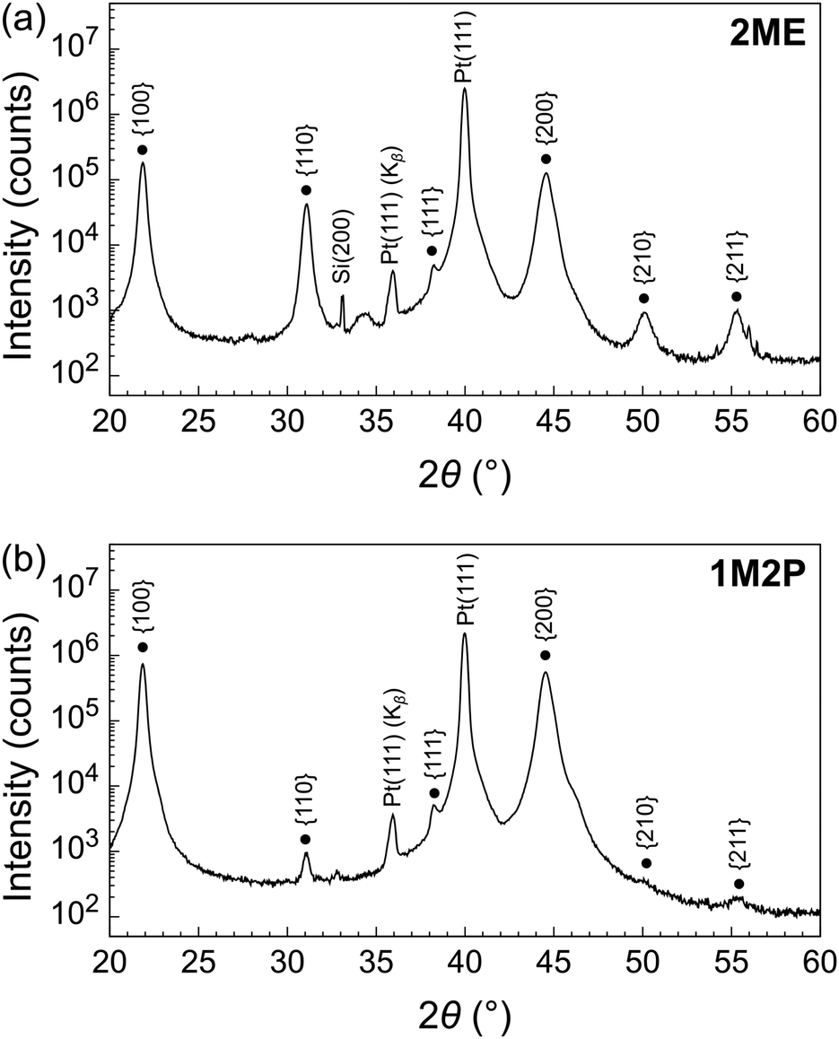 | ||
| Fig. 2 XRD patterns of micron-thick PZT thin films deposited on platinized silicon using (a) 2ME and (b) 1M2P-based solutions (PbTiO3 seed layer and PZT film). Note that the absolute scale is identical for both XRD patterns. A linear scale representation of these XRD patterns is shown in Fig. S2 (ESI†). | ||
The difference in the quality of the PZT orientation likely resides in the crystallization mechanism of the PZT layer, which is mediated by the PbTiO3 seed layer. To confirm that the seed layer induces the observed orientation effect, we performed a cross-check experiment by making a matrix of both layers deposited from different solvents, as illustrated in Fig. S1 in the ESI.† From the XRD patterns of 200 nm-thick PZT films spin-coated on PbTiO3 seed layers, it appears that the 1M2P-derived seed layer is indeed responsible for the strong {100} orientation in PZT, regardless of the solvent used for the deposition of the latter layer. We therefore proceeded with a closer examination of the microstructure of 2ME and 1M2P-derived seed layers in order to gain a deeper understanding of the solvent influence.
XRD patterns and surface SEM micrographs are shown in Fig. 3. The XRD peaks recorded in θ–2θ geometry and associated with the PbTiO3 phase have relatively low intensities as the seed layer is very thin. Substrate-related parasitic peaks are also present in the XRD patterns. However, it clearly appears that 1M2P-derived PbTiO3 seed layers exhibit a strong (100) orientation with a striking (100)/(001) peak splitting compared to the 2ME-derived ones. A marked difference also appears upon observation of the top surface by SEM. On the one hand, 2ME-derived seed layers consist of nanoislands, where individual PbTiO3 grains adopt irregular shapes. On the other hand, the use of 1M2P promotes the growth of PbTiO3 nanocrystal clusters with well-defined facets. Despite the apparent random orientation of these nanocrystals, it is clear from the XRD analysis that the (100)/(001) orientation prevails statistically. The 2:1 intensity ratio between the (100) and (001) peaks could be explained by stress relaxation of the stand-alone grains, in contrast with the 2ME-derived layers, where the (001) contribution is more pronounced. Indeed, PbTiO3 generally exhibits a negative coefficient of thermal expansion in the ferroelectric phase due to a strong decrease of the out-of-plane lattice parameter with increasing temperature.20,21 This in turn induces a compressive thermoelastic stress in PbTiO3 at room temperature, which favors the (001) orientation. The SEM top views together with the AFM measurements (respectively Fig. 3c and Fig. S5d, ESI†) show that the well-defined grains in 1M2P-derived PbTiO3 are well separated from each other (thus inducing stress relaxation) contrary to 2ME-derived PbTiO3. Out-of-plane piezoresponse force microscopy (PFM) analysis of the PbTiO3 seed layers was performed and results are shown in Fig. S5 (ESI†). In both cases PFM signal is present across the whole surface, proving that both layers are continuous.
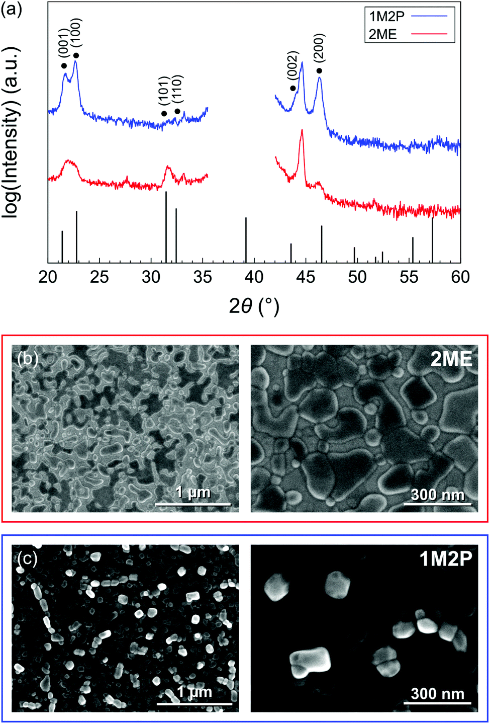 | ||
| Fig. 3 (a) XRD patterns of PbTiO3 seed layers deposited using 2ME and 1M2P-based solutions. The peak at ∼44.5° can be attributed to the substrate (see Fig. S3, ESI†), while the low-intensity peak at ∼28° could be associated to the (110) reflection of rutile (TiO2). A linear scale representation of these XRD patterns is shown in Fig. S4 (ESI†). SEM top views reveal the presence of (b) PbTiO3 nanoislands in the case of the 2ME-derived seed layer and (c) nanocrystals for the 1M2P-derived seed layer. | ||
Several explanations could be invoked to explain the differences in microstructures and orientations. First, it could be hypothesized that the amount of precursor material deposited on the substrate by spin coating could influence the growth of the crystalline phase. Due to the difference in rheological properties, we have determined in previous experiments that 1M2P-derived layers are approximately 5/4 times thicker than 2ME-derived films processed in the same conditions. We can estimate that the average thicknesses are ∼13 nm and ∼16 nm in the case of 2ME and 1M2P-derived seed layers, respectively. Assuming that the expected thickness of the liquid film is proportional to  (where ω is the angular velocity of spinning), we investigated the influence of the spinning rate (therefore amount of deposited material) on the microstructure of the seed layers. The results are presented in Fig. S6 (ESI†). It appears that adjusting the spinning rate such to deposit a similar amount of material does not have a significant influence on microstructure development. Interestingly, when the 1M2P-based PbTiO3 solution is spun at 4700 rpm, a greater amount of well-defined isolated nanocrystals can be seen on the surface (Fig. S6e, ESI†). In these conditions, the development of such different microstructures could be ascribed to different wetting interactions between the precursor solution and the substrate.
Another possible explanation could reside in solution chemistry. The different structures of 2ME and 1M2P likely result in different reactivities towards metal precursors. As a consequence, the species formed in solution upon mixing and refluxing presumably have different structures and distributions of the metal cations. According to Muralt, in the case of sputter-deposited PbTiO3 seed layers, crystallization of the (100) orientation was ascribed to a high partial pressure of PbO in the system.22 In the present case, we could hypothesize that the metal species obtained upon reaction with 1M2P possess lead-rich clusters that could in turn provide a lead-rich environment during crystallization, thus favoring the growth of the (100) orientation.
We also performed an experiment to study the influence of acetylacetone, which is added as a chelating agent for the stabilization of titanium(IV) isopropoxide. As can be seen in Fig. S7 (ESI†), the nanocrystal microstructure of the seed layer is only obtained upon combined use of 1M2P and acetylacetone. We can therefore conclude that the highly oriented seed layers result from a synergistic effect between 1-methoxy-2-propanol and acetylacetone.
In order to gain additional insights, we performed thermogravimetric analysis (TGA) coupled with differential thermal analysis (DTA) of powders obtained by drying the acetylacetone-based PbTiO3 solutions. The results presented in Fig. S8 (ESI†) reveal that the crystallization of the 2ME-derived PbTiO3 powder occurs at higher temperatures than its 1M2P-derived counterpart and follows a different crystallization path, as shown by exothermic contributions to the DTA signal. The decomposition of 2ME-derived powders and conversion into perovskite phase could proceed via carbonate species, which are undesired intermediates as they persist up to high temperatures (∼600 °C).23 The nature of the solvent participating as a metal ligand could influence the formation of carbonates. Indeed, the primary alcohol in 2ME could be oxidized to a carboxylic acid and undergo decarboxylation, which in turn would generate carbonates. The presence of a secondary alcohol in 1M2P could prevent this phenomenon. Further investigations would be required to verify this hypothesis and provide a better understanding of the crystallization mechanism.
3.3 Electrical and piezoelectric characterization
We then proceeded with the electrical and piezoelectric characterization of our 950 nm-thick PZT layers in order to study the influence of the solvent used in the process on the properties of the final layers. The polarization–electric field loops measured at 100 Hz are shown in Fig. 4a. Under normal measurement conditions (progressive increase of the maximum electric field), both samples exhibited similar properties with a remanent polarization Pr = 18 μC cm−2 and coercive field Ec = 35 kV cm−1. Interestingly, the prior application of higher electric fields (in the 0.7–1 MV cm−1 range) occasionally resulted in a wake-up effect of the ferroelectric capacitors, for which a remanent polarization as high as 30 and 37 μC cm−2 was measured for 2ME and 1M2P-derived films, respectively. The latter are also characterized by square-shaped loops, reminiscent of those of single crystals. Relative permittivity–electric field loops at 1 kHz are shown in Fig. 4b. The relative permittivity at zero bias reaches a value of εr = 1300, with losses tanδ remaining at 0.04, regardless of the solvent used.
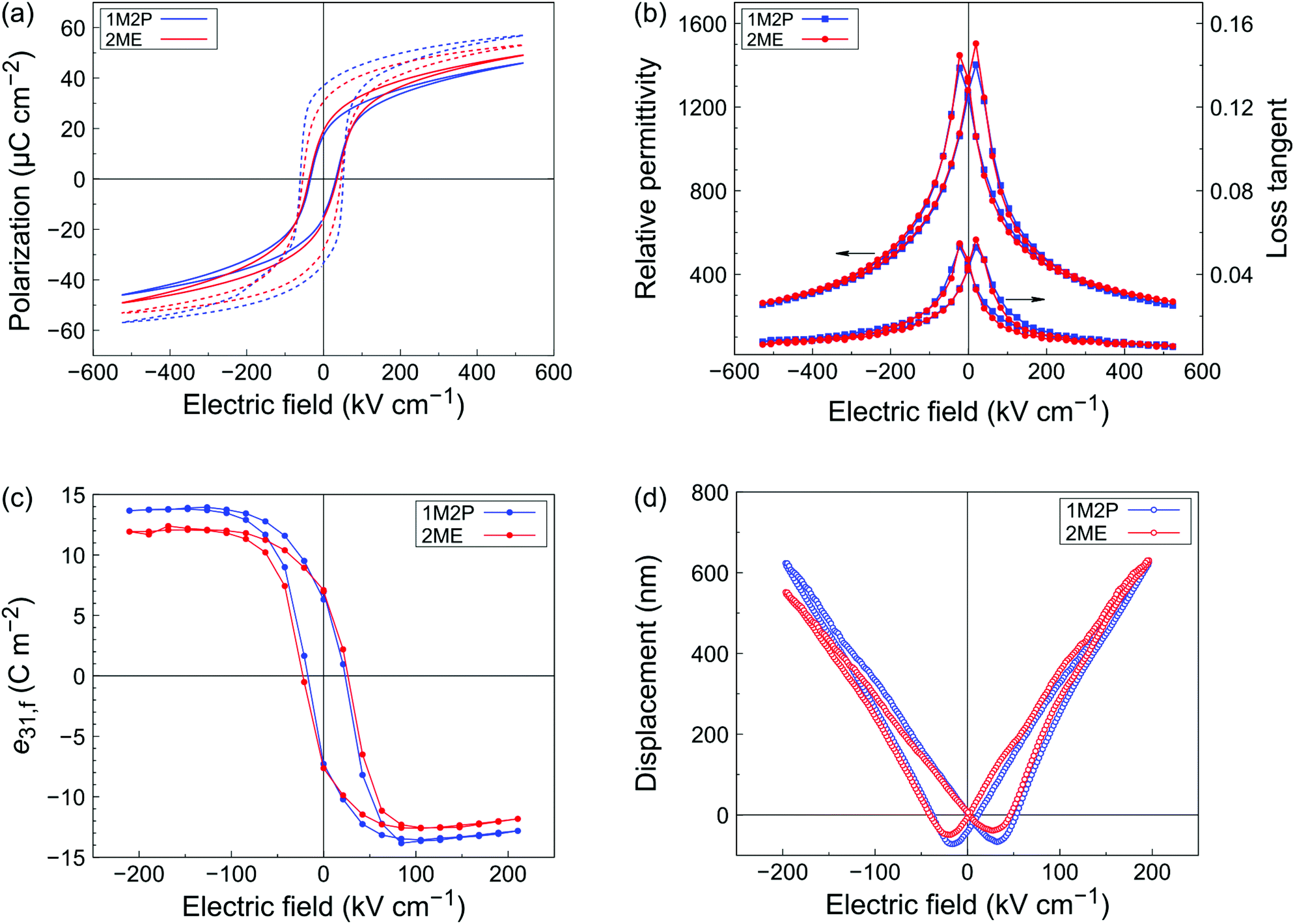 | ||
| Fig. 4 Electrical and piezoelectric characterization of spin-coated micron-thick PZT films obtained from 2ME and 1M2P-based precursor solutions. (a) Polarization–electric field loops at 100 Hz. The dashed lines show the polarization loops measured as a result of the wake-up effect. (b) Relative permittivity–electric field loops at 1 kHz (VAC = 500 mV). (c) e31,f coefficients as function of DC bias field measured via the 4PB method (10 Hz mechanical excitation) and (d) displacement–electric field butterfly loops (20 Hz electrical excitation). | ||
The effective transverse piezoelectric coefficient e31,f was evaluated via the four-point bending method.18Fig. 4c shows the evolution of the e31,f with a bias electric field. Films derived from 2ME and 1M2P-based solutions both exhibit a remanent piezoelectric coefficient close to 7 C m−2. However, the maximum values of the piezoelectric coefficient were noticeably higher for the 1M2P-derived sample, with ±13.8 C m−2, as compared to −12.6 C m−2 and 12.1 C m−2 for the 2ME-derived sample. A similar trend was observed when performing piezoelectric characterization via the converse method, where a 20 Hz electrical excitation was applied to the sample and the displacement was monitored as function of the electric field. The characteristic butterfly loops are shown in Fig. 4d. By performing a linear fitting in the −100 to 0 kV cm−1 range and using the formula from Mazzalai et al.19 we extracted values of −13.9 and −14.6 C m−2 for the 2ME and 1M2P-derived samples, respectively. An improvement of the electromechanical response up to 15% in the case of the sample fabricated through the 1M2P route could be ascribed to the improvement of the {100} orientation provided by the solvent. The e31,f values that we report are consistent with the ones obtained for typical CSD-derived {100}-textured PZT layers that feature a chemical gradient (see Fig. S9, ESI†).4,24 Note that the chemical gradient is quantitatively similar for both 2ME and 1M2P-derived layers, but more pronounced in the vicinity of the substrate for the 1M2P-derived PZT film, as shown in Fig. S10 (ESI†).
This last observation could account for the moderate improvement of the piezoelectric response, which results from the competition between orientation and chemical gradient. We speculate that a strong enhancement of the piezoelectric response could be achieved through multi-layered deposition of solutions with varying Zr/Ti ratios to counteract the development of the chemical gradient, as originally proposed by Calame and Muralt.24 However, this investigation is beyond the scope of the present study.
We can therefore conclude that 1-methoxy-2-propanol provides a suitable replacement to 2-methoxyethanol for the processing of PZT films, as the latter exhibit an enhanced electromechanical response that could be attributed to the strong {100} orientation induced by 1-methoxy-2-propanol-derived PbTiO3 seed layers. Moreover, 1M2P is a safe solvent, whereas 2ME is highly carcinogenic and teratogenic and therefore banned in industry.
4 Conclusions
In this work, we studied the influence of the solvent on the processing and ferro- and piezoelectric properties of PZT thin films. 2-Methoxyethanol and 1-methoxy-2-propanol were selected for the study, as 2-methoxyethanol is a popular though carcinogenic solvent for PZT processing and 1-methoxy-2-propanol has a similar structure, while none of the harmful effects. We discovered that the use of 1-methoxy-2-propanol enables the deposition of high-quality PZT layers whose electrical and piezoelectric properties are improved when compared those of layers obtained via the 2-methoxyethanol route and processed in similar conditions. The improvement could be ascribed to the high {100} orientation induced in the PZT films thanks to a highly oriented PbTiO3 seed layer derived for a 1-methoxy-2-propanol-based solution. We found that a synergistic effect between 1-methoxy-2-propanol and acetylacetone was responsible for the crystallization of PbTiO3 seed layers into a highly (100)/(001)-oriented nanocrystalline microstructure. Consequently, we believe that 1M2P could advantageously replace 2ME in PZT thin films processing because on the one hand, it is a safe solvent contrary to 2ME and on the second hand, PZT films processed this way exhibit better piezoelectric properties.Conflicts of interest
Processing details disclosed in the present contribution are protected by a patent filed in June 2020 (N. Godard, S. Glinšek, A. Blázquez Martínez, E. Defay, patent LU101884, 2020).Acknowledgements
The authors acknowledge financial support from the Luxembourg National Research Fund (FNR) under projects CO-FERMAT (FNR/P12/4853155/Kreisel) and HARVESTORE (FNR/INTER/ANR/18/12618689/Defay), and internal funding by the Luxembourg Institute of Science and Technology (LIST) under project SF_MRT-CSDFO. The authors wish to thank Stéphanie Girod and Aymen Mahjoub for the deposition and patterning of platinum top electrodes, Tony Schenk for XRD measurements, Nathalie Valle and Brahime El Adib for D-SIMS analyses, as well as Benoît Marcolini and Régis Vaudemont for thermal analyses.References
- E. Fortunato, P. Barquinha and R. Martins, Adv. Mater., 2012, 24, 2945–2986 CrossRef CAS.
- M. Jung, S.-G. Ji, G. Kim and S. I. Seok, Chem. Soc. Rev., 2019, 48, 2011–2038 RSC.
- P. Muralt, J. Micromech. Microeng., 2000, 10, 136–146 CrossRef CAS.
- N. Ledermann, P. Muralt, J. Baborowski, S. Gentil, K. Mukati, M. Cantoni, A. Seifert and N. Setter, Sens. Actuators, A, 2003, 105, 162–170 CrossRef CAS.
- N. Bassiri-Gharb, Y. Bastani and A. Bernal, Chem. Soc. Rev., 2014, 43, 2125–2140 RSC.
- S. Trolier-McKinstry and P. Muralt, J. Electroceram., 2004, 12, 7–17 CrossRef CAS.
- B. Malič and H. Suzuki, J. Ceram. Soc. Jpn., 2014, 122, 1–8 CrossRef.
- R. W. Schwartz, T. Schneller and R. Waser, C. R. Chim, 2004, 7, 433–461 CrossRef CAS.
- T. W. Dekleva, J. M. Hayes, L. E. Cross and G. L. Geoffroy, J. Am. Ceram. Soc., 1988, 71, 280–282 CrossRef.
- S. S. Sengupta, L. Ma, D. L. Adler and D. A. Payne, J. Mater. Res., 1995, 10, 1345–1348 CrossRef CAS.
- I. Arčon, B. Malič, M. Kosec and A. Kodre, J. Sol-Gel Sci. Technol., 1998, 13, 861–864 CrossRef.
- Z. Duan, X. Shi, Y. Cui, Y. Wan, Z. Lu and G. Zhao, J. Alloys Compd., 2017, 698, 276–283 CrossRef CAS.
- P. T. Tue, T. Shimoda and Y. Takamura, APL Mater., 2020, 8, 021112 CrossRef CAS.
- Y. Yao, A. B. Naden, F. Zhang, D. Edwards, P. Joshi, B. J. Rodriguez, A. Kumar and N. Bassiri-Gharb, J. Eur. Ceram. Soc., 2020, 40, 5369–5375 CrossRef CAS.
- Institut National de Recherche et de Sécurité (INRS), 2-Méthoxyéthanol (fiche toxicologique no. 103), 2014, http://www.inrs.fr/publications/bdd/fichetox/fiche.html?refINRS=FICHETOX_103.
- Institut National de Recherche et de Sécurité (INRS), 1-Méthoxy-2-propanol et son acétate (fiche toxicologique no. 221), 2010, http://www.inrs.fr/publications/bdd/fichetox/fiche.html?refINRS=FICHETOX_221.
- N. Godard, M. A. Mahjoub, S. Girod, T. Schenk, S. Glinšek and E. Defay, J. Mater. Chem. C, 2020, 8, 3740–3747 RSC.
- K. Prume, P. Muralt, F. Calame, T. Schmitz-Kempen and S. Tiedke, IEEE Trans. Ultrason. Eng., 2007, 54, 8–14 Search PubMed.
- A. Mazzalai, D. Balma, N. Chidambaram, R. Matloub and P. Muralt, J. Microelectromech. Syst., 2015, 24, 831–838 CAS.
- J. Chen, K. Nittala, J. S. Forrester, J. L. Jones, J. Deng, R. Yu and X. Xing, J. Am. Chem. Soc., 2011, 133, 11114–11117 CrossRef CAS.
- F. Wang, Y. Xie, J. Chen, H. Fu and X. Xing, Appl. Phys. Lett., 2013, 103, 221901 CrossRef.
- P. Muralt, J. Appl. Phys., 2006, 100, 051605 CrossRef.
- P. R. Coffman, C. K. Barlingay, A. Gupta and S. K. Dey, J. Sol-Gel Sci. Technol., 1996, 6, 83–106 CrossRef CAS.
- F. Calame and P. Muralt, Appl. Phys. Lett., 2007, 90, 062907 CrossRef.
Footnote |
| † Electronic supplementary information (ESI) available. See DOI: 10.1039/d0tc04066e |
| This journal is © The Royal Society of Chemistry 2021 |