
 Open Access Article
 This Open Access Article is licensed under a Creative Commons Attribution-Non Commercial 3.0 Unported Licence
Facile synthesis of copper selenides with different stoichiometric compositions and their thermoelectric performance at a low temperature range†
Longbin Lia,
Yifang Zhao a,
Chaosheng Shia,
Wei Zeng*a,
Bing Liaob,
Mingqiu Zhangc and
Xiaoming Taod
a,
Chaosheng Shia,
Wei Zeng*a,
Bing Liaob,
Mingqiu Zhangc and
Xiaoming Taod
aGuangdong Key Laboratory of Industrial Surfactant, Institute of Chemical Engineering, Guangdong Academy of Sciences, Guangzhou 510665, China. E-mail: zengwei@gdcri.com
bGuangdong Academy of Sciences, Guangzhou 510665, China
cKey Laboratory for Polymeric Composite and Functional Materials of Ministry of Education, GD HPPC Lab, School of Chemistry and Chemical Engineering, Sun Yat-Sen University, Guangzhou 510275, P. R. China
dResearch Centre for Smart Wearable Systems, Institute of Textiles and Clothing, The Hong Kong Polytechnic University, Hong Kong
First published on 28th July 2021
Abstract
Copper selenide is widely considered to be a promising candidate for high-performance flexible thermoelectrics; however, most of the reported ZT values of copper selenides are unsatisfactory at a relatively low temperature range. Herein, we utilized some wet chemical methods to synthesize a series of copper selenides. XRD, SEM and TEM characterizations revealed that CuSe, Cu3Se2 and Cu2−xSe were prepared successfully and possessed different morphologies and sizes. Based on the analysis of their thermoelectric properties, Cu2−xSe exhibited the highest Seebeck coefficient and lowest thermal conductivity among the three samples owing to its unique crystal structure. After being sintered at 400 °C under N2 atmosphere, the electrical conductivity of Cu2−xSe enhanced considerable, resulting in a significant improvement of its ZT values from 0.096 to 0.458 at 30 to 150 °C. This result is remarkable for copper selenide-based thermoelectric materials at a relatively low temperature range, indicating its brilliant potential in the field of flexible thermoelectric devices.
Introduction
In recent years, wearable and implantable electronic devices have been receiving increasing attention and further development for their multiple applications in various fields relating to human bodies, such as cardiac pacemakers, cochlear implants, gastric stimulators, physiological sensors, smart watches, and smart glasses.1 For the sake of extending the usage time of such devices effectively, researchers have proposed two main strategies: one is expanding the capacity of the power source used in the wearable devices, and the other is harvesting energy from the human body or the surrounding environment to fabricate the so-called self-powered devices.2 For the second construction method, the flexible thermoelectric (FTE) materials are considered promising candidates that meet the requirement well. The advantages of FTE materials in manufacturing such self-powered devices include: (a) they can operate well within physiological temperatures,3,4 and (b) their light weight allows the conformable attachment onto human skin or other organs to utilize the body heat maximally.5,6 Thus, FTE materials are convinced to play an increasingly important role in self-powered devices in the near future, and relevant researches are flourishing.Among the different types of inorganic thermoelectric (TE) materials, tellurides such as Bi2Te3 and PbTe are the most commonly studied and used nowadays.7–9 However, these tellurides contain rare-earth and toxic elements, thus driving researchers to develop alternative economical and eco-friendly TE materials with satisfactory TE properties.7 Compared with tellurium, selenium has a much higher earth abundance and is relatively less toxic. Hence, numerous selenides such as Cu2Se,10 SnSe,11,12 PbSe,13 In4Se3,14 Ag9GaSe6,15 and Cu3SbSe4 (ref. 16) have been introduced into TE application researches in recent years, and many of them have exhibited excellent TE performance. Cu2Se or Cu2−xSe is one of the most remarkable selenides in TE researches due to its unique crystal structure. In the high-temperature β-phase of Cu2−xSe, the Se atoms form a rigid crystalline sublattice while the copper ions are highly dispersed around the Se skeletons disorderly with liquid-like mobility.10 Such crystalline structure corresponds to the ideal phonon-glass electron-crystal model for high-efficiency TE materials. Besides, numerous types of synthesis methods have been applied in building copper selenide-based TE materials,17–30 some of which were even constructed as FTE devices.25,26 The morphology and TE performance of these copper selenides differ from each other to a certain degree under different synthesis conditions. To date, the highest ZT value of copper selenide-based TE materials has reached as high as 2.7,24 which is comparatively among the highest ZT values of all types of TE materials. However, many of the high ZT values of copper selenides are attained at very high temperatures, such as in the range of 800–1000 K. For FTE applications, it is usually supposed that the FTE devices should operate well near room temperature (RT) or at relatively low-temperature range. Nowadays, many of the reported ZT values of pure copper selenides are still less than 0.3 near RT.30 Thus, the TE performance of copper selenides needs further improvement at the relatively low-temperature range.
In this study, we utilized facile wet chemical methods for the synthesis of a series of copper selenide nanomaterials. The as-prepared copper selenide samples were first characterized by XRD, SEM and TEM tests. The results show that copper selenides with different stoichiometric compositions such as CuSe, Cu3Se2 and Cu2−xSe were successfully obtained via separate synthetic processes, and they possessed different morphologies and particle sizes. Further, TE performance tests were conducted between 30 and 150 °C, and the Cu2−xSe sample exhibited the highest Seebeck coefficient and the lowest thermal conductivity values among the three samples. After being sintered at 400 °C under an N2 atmosphere, the electrical conductivity of the Cu2−xSe sample significantly improved, and the highest ZT value reached about 0.46 at 150 °C, which is an impressive result for copper selenides at a relatively low temperature range.
Experimental section
Preparation of the copper selenides
Sample 1 (S1, CuSe): 0.33 g SeO2 and 1.5 g CuSO4·5H2O were first dissolved in 50 mL DI water. Then, 1.26 g Na2SO3 was added to the solution and stirred for 5 min. Then, the mixture was poured into a 100 mL stainless steel autoclave and heated to 80 °C for 12 h. After the hydrothermal reaction was completed, the obtained precipitates were rinsed with DI water and ethanol, followed by drying at 60 °C.Sample 2 (S2, Cu3Se2): 0.32 g Se and 1.26 g Na2SO3 were first mixed in 50 mL water and stirred for 1 h at 80 °C. After cooling down to RT, the mixture was filtered, and the supernatant was poured into a 50 mL solution containing 2 g CuSO4·5H2O. Then, the mixture was further stirred at RT for 2 h. After the reaction finished, the precipitates were rinsed with DI water and ethanol and dried at 60 °C.
Sample 3 (S3, Cu2−xSe): 0.33 g SeO2 and 1.5 g CuSO4·5H2O were first dissolved in 50 mL DI water, and then 2.0 g sodium ascorbate was dissolved in 30 mL DI water. After all the chemicals were completely dissolved, the sodium ascorbate solution was poured into the SeO2 and CuSO4 mixture solution, and the mixed solution was kept stirring for 2 h at RT. The mixture was allowed to rest for a few hours after stirring, and then the precipitates were washed with DI water and ethanol successively, and finally dried at 60 °C.
Sample 4 (S4, s-Cu2−xSe): S3 was placed into a tube furnace and sintered at 400 °C under an N2 atmosphere for 1 h. The heating rate was 10 °C min−1, and the N2 was flowing during both the heating and cooling processes.
Characterization and measurements of the copper selenide samples
The crystal structure of the samples was characterized by X-ray diffractometry (XRD, Rigaku9000, Rigaku Corporation, Japan). The morphology of the as-prepared powders was examined by field emission scanning electron microscopy (FE-SEM, SU8220, Hitachi, Japan). Further structural and phase identification were performed by transmission electron microscopy and high-resolution transmission electron microscopy (TEM and HRTEM, Talos F200s, FEI, USA).Seebeck coefficient and electrical conductivity of the samples were tested by Seebeck coefficient measurement (LSR-3, Linseis, Germany) at the range of 30 to 150 °C. The as-prepared powders were pressed into 1.3 cm wide disks for the test. The applied pressure was 10 MPa and lasted for 5 min. Thermal conductivity was directly measured by a thermal conductivity analyzer (TPS 2500S, Hot Disk, Sweden) at the range between 30 and 150 °C.
A temperature controller (TLTP-TEC2415D, TLT, China) was used to provide temperature difference, and an electrochemical workstation (CHI810D, Chenghua, China) was used to record and analyze the stimulated electric signals. The as-prepared powders were pressed into a 1.5 cm wide and 2.0 cm long rectangle-shaped bulk for the output voltage test, whereby the applied pressure was 10 MPa and lasted for 5 min.
Results and discussion
After being rinsed and dried, the as-prepared samples were characterized by XRD, and the results are shown in Fig. 1. Fig. 1(a) shows the XRD pattern of S1 (CuSe), and the red vertical lines reflect the standard diffraction peaks of mineral klockmannite CuSe (JCPDS card no. 34-0171). One can notice that the corresponding XRD peaks of CuSe tally with the standard peaks. Fig. 1(b) is the XRD pattern of S2 (Cu3Se2), and the standard diffraction peaks of mineral umangite Cu3Se2 (JCPDS card no. 47-1745) are also shown. Most of the corresponding XRD peaks can be identified as that of Cu3Se2, and the weak peak at about 39° probably belongs to Se (JCPDS card no. 27-0603). Fig. 1(c) and (d) show the XRD patterns of S3 (Cu2−xSe) and S4 (the sintered-Cu2−xSe), which matched well with the standard diffraction pattern of cubic mineral berzelianite Cu2−xSe (JCPDS card no. 06-0680). It is worth noting that s-Cu2−xSe maintained the phase consistency with Cu2−xSe, and its steep diffraction peaks indicate the improved crystallinity after the calcination treatment.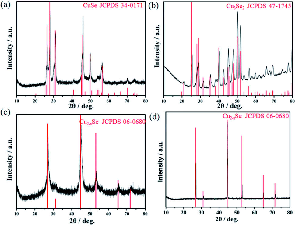 | ||
| Fig. 1 XRD patterns of the as-synthesized samples S1–S4 (a–d). | ||
Furthermore, the morphology and phase composition of the as-prepared copper selenide samples were characterized by SEM and TEM. Fig. 2(a) displays the SEM images of CuSe with different resolutions. It can be seen that the CuSe sample exhibits two types of morphologies, namely sphere-like and sheet-like morphologies. Thereinto, the particle sizes of the sheets are relatively large and their diameters are approximately from 2 to more than 5 μm. Respectively, the spheres are relatively smaller, with diameters ranging from about 200 to 700 nm. Different from CuSe, the particles of Cu3Se2 (Fig. 2(b)) are much smaller (diameters are less than 100 nm), and many of them can be recognized as wedge-like shapes, as shown in the zoomed image. Fig. 2(c) displays the SEM images of Cu2−xSe. It can be seen that Cu2−xSe also consists of nanoparticles with diameters less than 100 nm, but they are mostly round shapes seen from the zoomed image. However, the particle size and morphology of Cu2−xSe turn out to be quite different after calcination, as shown in Fig. 2(d). Clearly, all the nanoparticles disappeared and fused into a large bulk structure. The nanoparticles fused so well that no apparent cracks can be seen in the zoomed image.
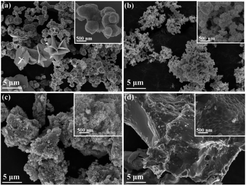 | ||
| Fig. 2 SEM images of (a) CuSe, (b) Cu3Se2, (c) Cu2−xSe, and (d) s-Cu2−xSe. | ||
More morphological information has been provided based on the TEM characterization. Fig. 3(a) and (d) show the TEM and HRTEM images of CuSe, respectively. Clearly, larger-sized sheets and smaller-sized spherical bulks can be seen in Fig. 3(a), which is consistent with the SEM result, as shown in Fig. 2(a). HRTEM images were obtained on both the sheets and the spherical bulks, and it is interesting to note that both structures share the same lattice distance of about 0.33 nm, as shown in Fig. 3(d). This lattice distance can be identified as the lattice spacing of the (101) plane in hexagonal klockmannite CuSe,31 indicating that the sample consists of pure CuSe with two different morphologies. TEM and HRTEM images of Cu3Se2 are shown in Fig. 3(b) and (e), respectively. The diameters of the nanoparticles of Cu3Se2 can be estimated more precisely to be about 15–30 nm from Fig. 3(b). Also, the wedge-like shapes of the nanoparticles can be recognized more clearly. Fig. 3(e) exhibits the HRTEM image of Cu3Se2, whereby the interplanar spacing is about 0.35 nm, which agrees well with the (101) planes of tetragonal umangite Cu3Se2.32 It can be seen in Fig. 3(c) and (f) that the diameters of the nanoparticles of Cu2−xSe were estimated at about 10–20 nm and its interplanar spacing is about 0.33 nm, which corresponds to the (111) planes of the cubic β-phase berzelianite of Cu2−xSe. Though our Cu2−xSe sample was synthesized at RT, it is confirmed to have a high-temperature β-phase structure instead of a low-temperature α-phase structure, whose interplanar spacing of the (111) planes should be doubled (about 0.66 nm) than that of the β-phase structure.10 This can be explained by the low α–β transition temperature of Cu2−xSe (about 340–400 K), which is very close to RT. Moreover, the nano-sized β-phase structure Cu2−xSe is considered to be more thermodynamically stable and commonly fabricated below 400 K.33 The imperfection of crystallinity of Cu2−xSe can also be seen in HRTEM in another resolution, as shown in the ESI (Fig. S1†).
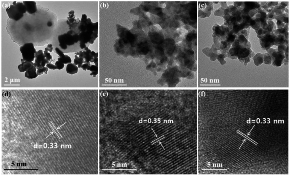 | ||
| Fig. 3 TEM and HRTEM images of CuSe (a and d), Cu3Se2 (b and e) and Cu2−xSe (c and f), respectively. | ||
The TE properties of the copper selenide samples, including Seebeck coefficient, electrical conductivity, and thermal conductivity, were then examined in the temperature range of 30–150 °C (about 303 to 423 K), and the ZT values were calculated based on these tests. The actual photos, surface SEM images, and EDX analysis results of the pressed samples are shown in the ESI (Fig. S2–S4†). First, the temperature dependencies of Seebeck coefficients of the samples, are shown in Fig. 4(a). Clearly, all the as-synthesized samples possessed positive Seebeck coefficients, indicating that they are all p-type TE materials. For the as-prepared CuSe, Cu3Se2 and Cu2−xSe samples, their Seebeck coefficients are in the range of 15.3–23.3 μV K−1, 17.2–29.1 μV K−1 and 25.8–46.6 μV K−1, respectively. It can be noticed that the order of Seebeck coefficients from high to low was Cu2−xSe > Cu3Se2 > CuSe. The differences in the Seebeck coefficients resulted from different crystal structures, thus giving rise to different electron band structures and electron scattering. Moreover, the Seebeck coefficient of the sintered Cu2−xSe (s-Cu2−xSe) has a slight increase compared to that of the original one, particularly above 360 K. The highest Seebeck coefficient value shown by s-Cu2−xSe was about 52.5 μV K−1 near 423 K.
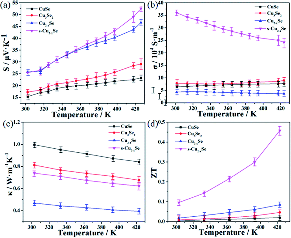 | ||
| Fig. 4 Temperature dependence of Seebeck coefficients (a), electrical conductivity (b), thermal conductivity (c) and ZT value (d) of the samples. | ||
Fig. 4(b) exhibits the electrical conductivity of these samples. The σ values of the three as-prepared copper selenide samples are close with each other in the measured temperature range, CuSe is about (6.1–7.6) × 104 S m−1, Cu3Se2 was (7.9–8.8) × 104 S m−1 and Cu2−xSe was (3.64.3) × 104 S m−1, respectively. However, after sintering, the σ value of s-Cu2−xSe significantly increased to about (24.4–36.3) × 104 S m−1, which was almost 10 times higher than that of the untreated Cu2−xSe sample. Sintering is widely utilized for accelerating the TE performance of the materials constructed by wet-chemistry methods as the crystallinity of Cu2−xSe can be effectively improved after sintering.18,21,31 This improvement can be verified by the XRD patterns, as shown in Fig. 1(c) and (d) in our study. In addition, based on the SEM images shown in Fig. 2(c) and (d), the Cu2−xSe nanoparticles fused densely into bulks after sintering, which leads to better electronic transportation pathways inside the material and further increase the electrical conductivity.
Thermal conductivity was examined at 303, 333, 363, 393 and 423 K, and the results are shown in Fig. 4(c). It can be seen that all the κ values of the samples are below 1.00 W m−1 K−1 in the measured temperature range, and they decrease with an increase in the temperature. The order of κ values of the three as-prepared samples from high to low is CuSe > Cu3Se2 > Cu2−xSe; CuSe is about 0.84–0.99 W m−1 K−1, Cu3Se2 is 0.68–0.81 W m−1 K−1, and Cu2−xSe is 0.39–0.47 W m−1 K−1. Among them, the κ value of Cu2−xSe is less than half of the other two samples. This result indicates that Cu2−xSe is the best TE material candidate among the three copper selenides with different stoichiometric compositions, which agrees with the results reported by other researchers focusing on copper selenides. The relatively low thermal conductivity of Cu2−xSe can be due to its unique crystal phonon-glass electron-crystal structure. In the cubic β-phase structure, the Cu ions are superionic and kinetically disordered throughout the phase structure, which can enhance the scattering of phonons and finally decrease the thermal conductivity.10 Conversely, neither CuSe, Cu3Se2 nor the α-phase Cu2−xSe is convinced to have such liquid-like Cu ions. Besides, the imperfection of crystallinity of the as-prepared Cu2−xSe sample, which can be seen from the XRD (Fig. 1(c)) and HR-TEM (Fig. 3(f)) tests, also leads to its relatively low thermal conductivity. Though sintering is beneficial for obtaining better Seebeck coefficient and electrical conductivity results for the as-prepared Cu2−xSe sample, the κ value of s-Cu2−xSe unfavorably increases to about 0.62–0.74 W m−1 K−1 compared to that of the untreated one, and the TE performance is affected simultaneously. This may be ascribed to the bulk structure evolved from the nanoparticles after sintering, which is beneficial to promote the transportation of not only the electrons but also the phonons and result in an increase in both electrical and thermal conductivity.
The eventual calculated ZT values of the samples are shown in Fig. 4(d). All the ZT values of the samples increase with the increase in temperature. The ZT values of CuSe and Cu3Se2 are about 0.004–0.021 and 0.009–0.046, respectively. Owing to the higher Seebeck coefficient and lower thermal conductivity, the ZT values of the as-prepared Cu2−xSe increased slightly to 0.018–0.085 compared to that of the other two samples. After sintering, the ZT values of s-Cu2−xSe significantly increased to about 0.096–0.458. Undoubtedly, this is mainly by virtue of the enormous improvement of its electrical conductivity. This ZT value of s-Cu2−xSe is also impressive for pure copper selenide TE materials at the relatively low temperature range. The EDX analysis results (shown in Fig. S3†) reveal that the x values of Cu2−xSe and s-Cu2−xSe are 0.22 and 0.16, respectively. The x value of Cu2−xSe is slightly larger than the reported range (0.15 ≤ x ≤ 0.2),34 which indicates more amounts of Cu vacancies and limits the improvement of TE performance.30 To further improve the ZT values, nanostructure engineering and elemental doping are considered to be the effective strategies.35–37
The output voltage test of the sintered-Cu2−xSe sample was then investigated at 303 K. Fig. 5(a) shows the voltage–time curve of the sintered sample during heating. In the heating test, T1 was set as the cold side and stayed at 303 K. In contrast, T2 was set as the hot side and initially set at 303 K, followed by a successive increase of 10 K every 5 minutes with the temperature difference from 0 to 110 K. As shown in Fig. 5(a), the voltage–time curve of s-Cu2−xSe exhibited a well-defined step-shape, and the corresponding platforms for each temperature differences were relatively flat and stable. This result shows that the generated voltage as a function of temperature difference also exhibited excellent linearity, which is consistent with the Seebeck coefficient test and is beneficial for application in self-powered temperature sensors.38,39
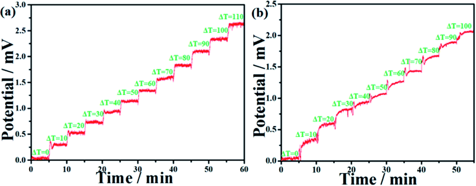 | ||
| Fig. 5 V–T curves of the s-Cu2−xSe sample under heating (a) and cooling (b) processes, respectively. | ||
At the cooling test of the output voltage, T1 and T2 were initially set at 353 K. Then, the hot side (T2) stayed at 353 K while the cold side (T1) successively decreased by 10 K every 5 min and eventually reached 253 K. As shown in Fig. 5(b), the cooling curve is also step-shape and increases with the increase in the temperature difference. However, the platforms are not so flat and stable compared with that of the heating curve, and the values of generated voltages are lower than that in the heating process under the same temperature difference. It may be due to the relatively slow response of the bulk sample while cooling.40
In addition, compared with some commonly used high-temperature synthesis methods for copper selenides which usually conduct as high as 1000 K and last about several days,10,17,19,20 the wet chemical methods are evidently much more time- and energy-saving. It is also worth noting that the reductant sodium ascorbate for the fabrication of Cu2−xSe, which we used here, is relatively environment-friendly and less toxic compared with other reductants such as NaBH4 and N2H4·2H2O that are used in other reported wet chemical methods.18,21 Hence, herein, we provided a facile, safe and environment-friendly way to fabricate Cu2−xSe materials with high TE performance at a relatively low temperature range.
Conclusion
In summary, facile wet-chemistry methods were applied to the synthesis of copper selenides. XRD, SEM and TEM measurements demonstrate that copper selenides with different stoichiometric compositions, such as CuSe, Cu3Se2 and Cu2−xSe, were obtained, and they differed in morphologies and sizes with each other. Among the three samples, Cu2−xSe exhibited the highest Seebeck coefficient and the lowest thermal conductivity, which can be attributed to its unique phonon-glass electron-crystal structure. After sintering, the Cu2−xSe sample attained better crystallinity and effective electronic transportation pathways, leading to a slight enhancement of the Seebeck coefficient and an enormous improvement in electrical conductivity. Though the thermal conductivity of sintered-Cu2−xSe rises as well, the eventual calculated ZT values of sintered-Cu2−xSe are much higher than that of the Cu2−xSe sample without sintering. The highest ZT value of sintered-Cu2−xSe is about 0.46 at 150 °C, which is a remarkable result for copper selenides-based TE material at a relatively low temperature range.Conflicts of interest
There are no conflicts of interest to declare.Acknowledgements
This work has been partially supported by the National Natural Science Foundation of China (Grant No. 52073066), the GDAS Project of Science and Technology Development (No. 2020GDASYL-20200102028, No. 2020GDASYL-20200103130, No. 2020GDASYL-20200102029 and No. 2018GDASCX-0116), and the Science and Technology Program of Guangdong Province (No. 2020B0101340005).References
- Y. Wang, L. Yang, X. Shi, X. Shi, L. Chen, M. S. Dargusch, J. Zou and Z. Chen, Adv. Mater., 2019, 31, 1807916 CrossRef PubMed.
- D. Jiang, B. Shi, H. Ouyang, Y. Fan, Z. L. Wang and Z. Li, ACS Nano, 2020, 14, 6436–6448 CrossRef CAS PubMed.
- C. Li, F. Jiang, C. Liu, P. Liu and J. Xu, Appl. Mater. Today, 2019, 15, 543–557 CrossRef.
- Q. Yao, Q. Wang, L. Wang and L. Chen, Energy Environ. Sci., 2014, 7, 3801–3807 RSC.
- C. S. Kim, G. S. Lee, H. Choi, Y. J. Kim, H. M. Yang, S. H. Lim, S. G. Lee and B. J. Cho, Appl. Energy, 2018, 214, 131–138 CrossRef.
- P. Zong, R. Hanus, M. Dylla, Y. Tang, J. Liao, Q. Zhang, G. J. Snyder and L. Chen, Energy Environ. Sci., 2017, 10, 183–191 RSC.
- W. Liu, L. Yang, Z. Chen and J. Zou, Adv. Mater., 2020, 32, 1905703 CrossRef CAS PubMed.
- C. Gayner and K. K. Kar, Prog. Mater. Sci., 2016, 83, 330–382 CrossRef CAS.
- T. Wei, C. Wu, F. Li and J. Li, J. Materiomics, 2018, 4, 304–320 CrossRef.
- H. Liu, X. Shi, F. Xu, L. Zhang, W. Zhang, L. Chen, Q. Li, C. Uher, T. Day and G. J. Snyder, Nat. Mater., 2012, 11, 422–425 CrossRef CAS PubMed.
- L. Zhao, S. Lo, Y. Zhang, H. Sun, G. Tan, C. Uher, C. Wolverton, V. P. Dravid and M. G. Kanatzidis, Nature, 2014, 508, 373–377 CrossRef CAS PubMed.
- J. Fan, X. Huang, F. Liu, L. Deng and G. Chen, Compos. Commun., 2021, 24, 100612 CrossRef.
- L. Zhao, S. Hao, S. Lo, C. Wu, X. Zhou, Y. Lee, H. Li, K. Biswas, T. P. Hogan, C. Uher, C. Wolverton, V. P. Dravid and M. G. Kanatzidis, J. Am. Chem. Soc., 2013, 135, 7364–7370 CrossRef CAS PubMed.
- J. Rhyee, K. H. Lee, S. M. Lee, E. Cho, S. I. Kim, E. Lee, Y. S. Kwon, J. H. Shim and G. Kotliar, Nature, 2009, 459, 965–968 CrossRef CAS PubMed.
- S. Lin, W. Li, S. Li, X. Zhang, Z. Chen, Y. Xu, Y. Chen and Y. Pei, Joule, 2017, 1, 816–830 CrossRef CAS.
- Y. Liu, G. García, S. Ortega, D. Cadavid, P. Palacios, J. Lu, M. Ibáñez, L. Xi, J. D. Roo, A. M. López, S. Martí-Sánchez, I. Cabezas, M. de la Mata, Z. Luo, C. Dun, O. Dobrozhan, D. L. Carroll, W. Zhang, J. Martins, M. V. Kovalenko, J. Arbiol, G. Noriega, J. Song, P. Wahnón and A. Cabot, J. Mater. Chem. A, 2017, 5, 2592–2602 RSC.
- H. Liu, X. Yuan, P. Lu, X. Shi, F. Xu, Y. He, Y. Tang, S. Bai, W. Zhang, L. Chen, Y. Lin, L. Shi, H. Lin, X. Gao, X. Zhang, H. Chi and C. Uher, Adv. Mater., 2013, 25, 6607–6612 CrossRef CAS PubMed.
- D. Li, X. Y. Qin, Y. F. Liu, C. J. Song, L. Wang, J. Zhang, H. X. Xin, G. L. Guo, T. H. Zou, G. L. Sun, B. J. Ren and X. G. Zhu, RSC Adv., 2014, 4, 8638–8644 RSC.
- A. A. Olvera, N. A. Moroza, P. Sahoo, P. Ren, T. P. Bailey, A. A. Page, C. Uher and P. F. P. Poudeu, Energy Environ. Sci., 2017, 10, 1668–1676 RSC.
- S. Butt, M. U. Farooq, W. Mahmood, S. Salam, M. Sultan, M. A. Basit, J. Ma, Y. Lin and C. Nan, J. Alloys Compd., 2019, 786, 557–564 CrossRef CAS.
- Q. Hu, Z. Zhu, Y. Zhang, X. Li, H. Song and Y. Zhang, J. Mater. Chem. A, 2018, 6, 23417–23424 RSC.
- W. Liao, L. Yang, J. Chen, D. Zhou, X. Qu, K. Zheng, G. Han, J. Zhou, M. Hong and Z. Chen, Chem. Eng. J., 2019, 371, 593–599 CrossRef CAS.
- J. Lei, Z. Ma, D. Zhang, Y. Chen, C. Wang, X. Yang, Z. Cheng and Y. Wang, J. Mater. Chem. A, 2019, 7, 7006–7014 RSC.
- D. Yang, X. Su, J. Li, H. Bai, S. Wang, Z. Li, H. Tang, K. Tang, T. Luo, Y. Yan, J. Wu, J. Yang, Q. Zhang, C. Uher, M. G. Kanatzidis and X. Tang, Adv. Mater., 2020, 32, 2003730 CrossRef CAS PubMed.
- Z. Lin, C. Hollar, J. S. Kang, A. Yin, Y. Wang, H. Shiu, Y. Huang, Y. Hu, Y. Zhang and X. Duan, Adv. Mater., 2017, 29, 1606662 CrossRef PubMed.
- Y. Lu, Y. Ding, Y. Qiu, K. Cai, Q. Yao, H. Song, L. Tong, J. He and L. Chen, ACS Appl. Mater. Interfaces, 2019, 11, 12819–12829 CrossRef CAS PubMed.
- S. Ballikaya, H. Chi, J. R. Salvadorc and C. Uher, J. Mater. Chem. A, 2013, 1, 12478–12484 RSC.
- T. Zhang, Y. Song, X. Zhang, X. He and J. Jiang, Mater. Lett., 2019, 250, 189–192 CrossRef CAS.
- L. Yang, J. Wei, Y. Qin, L. Wei, P. Song, M. Zhang, F. Yang and X. Wang, Materials, 2021, 14, 2075 CrossRef PubMed.
- J. Tak, W. H. Nam, C. Lee, S. Kim, Y. S. Lim, K. Ko, S. Lee, W. Seo, H. K. Cho, J. Shim and C. Park, Chem. Mater., 2018, 30, 3276–3284 CrossRef CAS.
- X. Liu, X. Duan, P. Peng and W. Zheng, Nanoscale, 2011, 3, 5090–5095 RSC.
- Q. Wang, Mater. Lett., 2009, 63, 1493–1495 CrossRef CAS.
- F. Gao, S. L. Leng, Z. Zhu, X. J. Li, X. Hu and H. Z. Song, J. Electron. Mater., 2018, 47, 2454–2460 CrossRef CAS.
- V. M. Garcia, P. K. Nair and M. T. S. Nair, J. Cryst. Growth, 1999, 203, 113–124 CrossRef CAS.
- Z. Zhu, Y. Zhang, H. Song and X. Li, Appl. Phys. A, 2019, 125, 572 CrossRef CAS.
- Z. Zhu, Y. Zhang, H. Song and X. Li, Appl. Phys. A, 2018, 124, 871 CrossRef.
- Y. Qin, L. Yang, J. Wei, S. Yang, M. Zhang, X. Wang and F. Yang, Materials, 2020, 13, 5704 CrossRef CAS PubMed.
- X. Chen, Z. Ren, H. Guo, X. Cheng and H. Zhang, Appl. Phys. Lett., 2020, 116, 043902 CrossRef CAS.
- M. Li, J. Chen, W. Zhong, M. Luo, W. Wang, X. Qing, Y. Lu, Q. Liu, K. Liu, Y. Wang and D. Wang, ACS Sens., 2020, 5, 2545–2554 CrossRef CAS PubMed.
- W. Zeng, X. Tao, S. Lin, C. Lee, D. Shi, K. Lam, B. Huang, Q. Wang and Y. Zhao, Nano Energy, 2018, 54, 163–174 CrossRef CAS.
Footnote |
| † Electronic supplementary information (ESI) available. See DOI: 10.1039/d1ra04626h |
| This journal is © The Royal Society of Chemistry 2021 |