
 Open Access Article
 This Open Access Article is licensed under a Creative Commons Attribution-Non Commercial 3.0 Unported Licence
A novel and facile synthesis strategy for highly stable cesium lead halide nanowires†
Ranran Zhoua,
Chi-An Chengc,
Siying Qiua,
Jiayi Chena,
Kun Nie *a,
Mengyun Wua,
Panlong Lina,
Hua Wang*a,
Luoxin Wanga and
Lefu Meib
*a,
Mengyun Wua,
Panlong Lina,
Hua Wang*a,
Luoxin Wanga and
Lefu Meib
aSchool of Materials Science and Engineering, Key Laboratory of Polyphenylene Sulfide Fiber and Application in Textile Industry, State Key Laboratory of New Textile Materials & Advanced Processing Technology and Key Laboratory of Textile Fiber and Products (Ministry of Education), Wuhan Textile University, 430200 Wuhan, P. R. China. E-mail: nkniekun@126.com; huawangabc@163.com
bBeijing Key Laboratory of Materials Utilization of Nonmetallic Minerals and Solid Wastes, National Laboratory of Mineral Materials, School of Materials Science and Technology, China University of Geosciences (Beijing), 100083 Beijing, P. R. China
cDepartment of Bioengineering, University of California Los Angeles, Los Angeles, California, USA
First published on 25th August 2021
Abstract
As promising low-dimensional semiconductor materials, cesium lead halide (CsPbX3, X = Cl, Br, I) perovskite-like nanowires (NWs) can be widely applied to the field of semiconductor devices and integrated optoelectronics. Therefore, developing a facile and efficient synthesis method of cesium lead halide perovskite-like NWs can bring both fundamental and practical impacts to the field of optoelectronics. Here, we developed a synthesis strategy of all-inorganic cesium lead halide CsPbI3 perovskite-like NWs under catalyst-free, solution-phase, and low-temperature conditions. The synthesis strategy was designed such that no inert gas is required and thus enables the synthesis to be carried out in air, which significantly reduces temperature, steps, time, and cost required for the reaction. The as-synthesized NWs were 7 μm in length and 80–100 nm in diameter with ideal morphology. Most of the CsPbI3 NWs were crystallized in orthorhombic phases that were arranged orderly with a uniform growth direction. In addition, the CsPbI3 NWs showed a photoluminescence peak near 610 nm and the fluorescence lifetime was 7.34 ns. The photoluminescence mechanism of CsPbI3 NWs involves the self-trapping behaviour in the radiative recombination process. The composition of CsPbI3 NWs is highly related to the synthesis temperature. The facile synthesis strategy has opened up a novel path for the synthesis of perovskite-like NWs, laying the foundation for the application of nano-optoelectronic devices, fluorescent anti-counterfeiting, and fluorescent composite materials.
1. Introduction
Metal halide perovskite-like materials with ABX3 structure (A = Rb, Cs; B = Ge, Sn, Pb; X = Cl, Br, I) have been widely used in solar cells,1–4 light-emitting diodes (LEDs),5–8 photodetectors,9–13 lasers14–17 and other fields because of their excellent optical and electrical properties, low cost preparation, and simple solution processing, and thus have attracted widespread attention in recent years.18 Compared to traditional semiconductor nanocrystals or nano-structured metal halide perovskite-like materials, all-inorganic lead halide perovskite-like materials (APbX3 (X = Cl, Br, I)) have better optical properties, including photoluminescence effect and a narrow emission peak width. In addition, the emission spectra can be adjusted to the entire visible region simply by modulating chemical components or changing the luminescence band size. Cesium lead iodide perovskite-like (CsPbI3), specifically, has a suitable band gap with fluorescent properties that achieve high luminescence efficiency and performance.19 The excellent physical properties of CsPbI3 have also prompted researchers to explore its use in high-performance optoelectronic applications.Various methods to synthesize CsPbX3 (X = Cl, Br, I) nanocrystals have been reported. Protesescu et al. first utilized a hot injection method to synthesize CsPbX3.20 Different nanostructures of CsPbX3 nanocrystals, including nanocubes (NCs), nanosheets (NSs), nanoplates (NPLs), quantum dots (QDs),21,22 and nanowires (NWs),23–25 have been synthesized by varying ligands26 and ratio, reaction time, or reaction temperature. The common synthesis method of CsPbX3 nanocrystals involves using a standard anaerobic Schlenk line device at high temperatures (140–200 °C), with the use of inert gas and vacuum drying environment.27 However, this common method does not apply well to all nanostructures of CsPbX3 nanocrystals. For example, although the NWs synthesized by the common method have excellent luminescence properties, the synthesis process is complex and costly. Moreover, the synthesis of CsPbI3 NWs requires higher temperature (most requires higher than 180 °C) than that required for CsPbBr3 NWs and CsPbCl3 NWs.28 Therefore, it is important to develop a facile and low-temperature synthesis method for CsPbI3 NWs.
Here, a novel and facile synthesis strategy for highly stable cesium lead halide nanowires (CsPbX3, X = Cl, Br, I) is reported. Compared with the conventional synthesis technique, our synthesis strategy uses a lower reaction temperature and does not require inert gas, vacuuming, and degassing processes. Our synthesis strategy with simplified reaction steps not only reduces the cost and time, but also improves the efficiency of the CsPbX3 synthesis. The as-synthesized CsPbI3 NWs using our strategy are formed as single crystals that crystallize in an orthorhombic phase and uniform growth directions. Also, the CsPbI3 NWs were demonstrated to have superior optical properties. In sum, this novel and facile synthesis method is ideal to study the structure–function relationship, which is highly important for the applications and development of nano-optoelectronics and semiconductor devices.29
2. Results and discussion
The preparation of CsPbI3 NWs was performed under air-free conditions. The preparation process did not require the participation of an inert gas, and the vacuuming and drying processes were omitted in the experiment. The scheme of the CsPbI3 NW preparation is shown in Fig. 1. Basically, the reaction was carried out by reacting Cs-oleic acid (Cs-OA) with lead halide (PbI2) in the presence of OA and oleylamine (OAm) in octadecene (ODE). Different reaction temperatures were first tested and optimized at 155 °C based on the diameter of the CsPbI3 NWs. Then, different reaction times at this temperature were tested and the reacted solution was cooled to room temperature on an ice-water bath. The as-synthesized nanocrystalline was obtained via centrifugation and purification and its morphology was examined via X-ray diffraction (XRD) and scanning electron microscopy (SEM).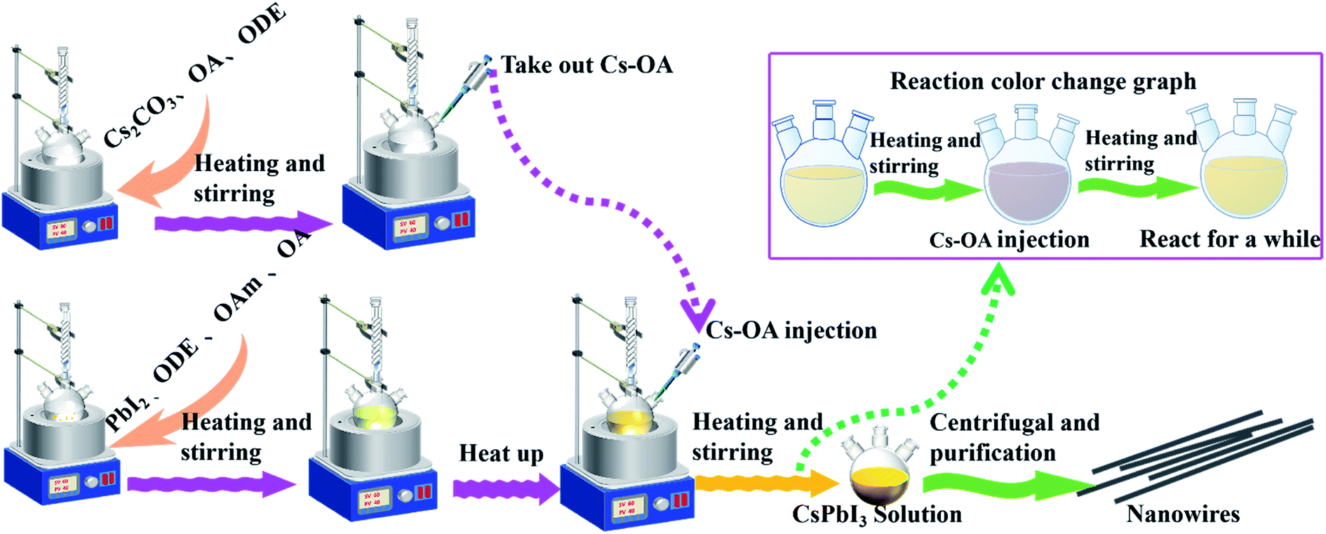 | ||
| Fig. 1 Scheme of CsPbI3 NWs preparation. | ||
The dynamics of CsPbI3 NW formation was studied via SEM. In the initial reaction stage (t < 10 min), the major morphology of the nanocrystalline was nanocube with the size ranging from 3 nm to 9 nm. After 10 min, a few CsPbI3 NWs with diameters around 100 nm and the length of about 3 μm were observed (Fig. 2(a)). After a longer reaction time (15–30 min), an increasing number of CsPbI3 NWs were formed with a longer length of about 7 μm (Fig. 2(b) and (c)), and the formed CsPbI3 NWs arranged more orderly (Fig. 2(d)). However, when the reaction time reached 30 min, the length of the CsPbI3 NWs began to shorten gradually while maintaining the ordered arrangement (Fig. 2(e) and (f)). Accordingly, the optimized reaction temperature of 155–160 °C and the optimized reaction time of 15–30 min will be used for the synthesis of all-inorganic CsPbI3 NWs, which leads to ideal morphology, ordered arrangement, and high crystallinity. Compared with CsPbI3 NWs with diameters ranging from tens to hundreds of nanometers,28 the CsPbI3 NWs synthesized here were more stable with a controllable diameter to about 100 nm. The HR-TEM images (ESI, Fig. S5†) show that the CsPbI3 NWs are single-crystalline.
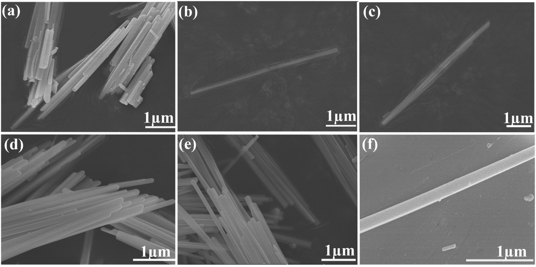 | ||
| Fig. 2 Synthesis of CsPbI3 NWs. (a) The reaction time is 10 min. (b–d) The reaction time is set as 15, 20 and 25 min, respectively. (e and f) The reaction time is 30 min. The images represent the morphological characterization of CsPbI3 NWs. Scale bar, 1 μm. | ||
The SEM image (ESI, Fig. S4†) and Fig. 3 show the evolution of CsPbI3 NWs. In the initial stage of the reaction, nanowires mainly exist in the form of nanocubes. Simultaneously, some nanocubes began to evolve. Fig. 4 shows that intermediates precursors similar to nanowires are derived from the interior of the nanocube. In addition, from Fig. 2, it is suggested that the derivatives of nanocubes are embryonic nanowires. As the reaction progresses, the NWs fall off from the inside of the nanocubes, and as the reaction time increases, the morphology of NWs is complete. No discrete reaction intermediates of CsPbI3 NWs were formed at a specific reaction time, as observed from the above experiments. Different intermediates coexisted with the product at a given reaction time. The growth and shape control of perovskite-like nanoparticles is a kinetically-controlled process, related to the binding of ligands and the temperature-dependent dynamic of surface ligands. The formation of perovskite-like nanoparticles is mainly divided into two steps. The first step involves a seed-mediated nucleation, and the second step involves further growth through self-assembly30 and the directed attachment. The lead component helps stabilize the nucleation of the perovskite-like structure. In addition, the aging of the precursor solution could promote the generation of CsPbI3 NWs.31
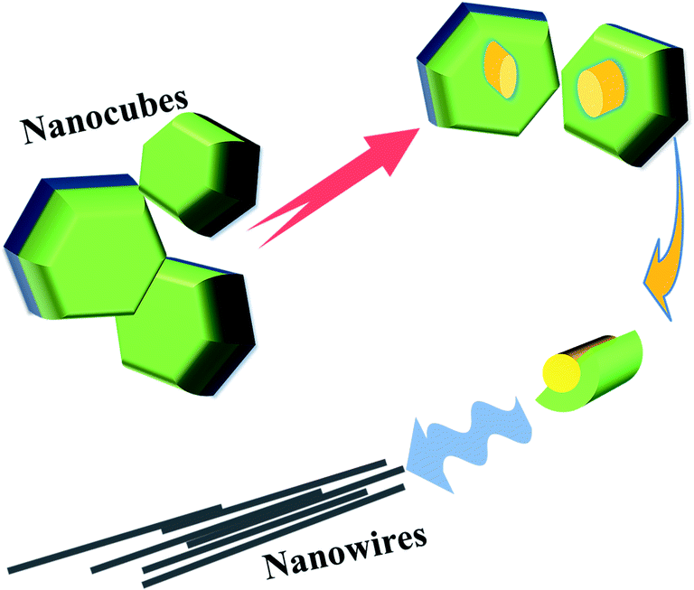 | ||
| Fig. 3 The evolution of CsPbI3 NWs. | ||
Another characteristic of the synthesis of CsPbI3 is the colour change during the synthesis. As the Cs-OA solution was added to the PbI2 precursor solution, the colour of the solution instantly turned reddish black, and then gradually changed to yellow with the increase in the reaction time and stayed yellow (Fig. 4(a)). The synthesized CsPbI3 NWs with simplified experimental steps show higher intensity of diffraction peaks in the XRD pattern, where the peaks correspond to the peaks in the spectrum of standard orthorhombic CsPbI3 (PDF # 741970) materials. In addition, the intensity of the diffraction peaks of CsPbI3 NWs gradually increased with time, which can be attributed to increase in time and coordination of anions and cations in the reaction solution,32 thereby promoting the growth and crystallinity of perovskite-like crystals. The results suggested that even if the experimental steps are simplified, the crystallinity of CsPbI3 NWs is still excellent and belongs to the orthorhombic phase. In addition, with the colour changed from reddish black to yellow in the reaction solution, CsPbI3 NWs were shown to undergo a phase transition33,34 from cubic phase to orthorhombic phase during the formation process. The characterization further supports that the synthesized CsPbI3 NWs have good morphology and completed crystal morphology.
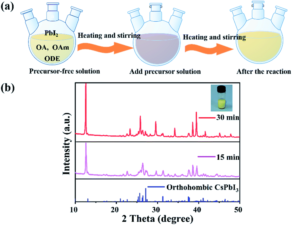 | ||
| Fig. 4 (a) Colour change of solution after adding precursor. (b) Standard XRD patterns (bottom) of orthorhombic CsPbI3, and experimental XRD patterns (top two) of CsPbI3 NWs. The pink colour is the reaction time of 15 min, the red colour is the reaction time of 30 min, respectively. Inset: CsPbI3 NWs distributed in hexane solution, showing yellow colour. | ||
Perovskite-like nanocrystals emit luminescence through the radiative recombination process of which the capture of a free electron by an ion occurs and an excess energy is radiated as photons.35,36 Defect states of traditional nanocrystals have energy levels in between the conduction band and the valence band and thus reduces the luminescence efficiency. In contrast, the energy levels of defect states of perovskite-like CsPbX3 nanoparticles are only formed inside the valence band and conduction band, avoiding the generation of intermediate state defects, thereby improving the luminescence efficiency.37,38 Therefore, compared with traditional luminescent materials, perovskite-like materials possess the advantages of narrow and symmetrical emission spectrum, controllable emission wavelength, high luminescence efficiency, and stable luminescence performance, making it an ideal luminescent material.
We further examined the optical properties of the experimentally synthesized CsPbI3 NWs. The photoluminescence spectra and fluorescence lifetime spectrum of the CsPbI3 NWs were measured at the optimized temperature during synthesis. Fig. 5(a) shows how the photoluminescence emission (PL) spectra of CsPbI3 NWs changed at 15 min, 20 min, and 25 min of reaction times. The formation of the NWs morphology was complete, as suggested by the single peak in the spectra. PL spectra (λex = 305 nm) of CsPbI3 NWs show broad bands from 400 to 750 nm. The fluorescence intensity increased with the increase in the reaction time. As time rises from 15 to 25 min, the peak in the PL spectra red-shifted from 603 nm to 609 nm, suggesting that the nanoparticles became larger as the time increased. The red-shift phenomenon can be attributed to the effects of the local state energy level on the emission of the CsPbI3 NWs, thereby affecting the quantum confinement.39,40 In addition, the emission peak is symmetrically distributed and narrow, which indicates that the size distribution of the CsPbI3 NWs is uniform and thus the NWs are mono-dispersed. The photoluminescence excitation (PLE) spectra (λem = 606 nm) in Fig. 5(b) shows the excitation bands peaked around 305 nm. The peak of 25 min was stronger than the peak of 15 min, and the peak intensity also increased over time, further indicating that the size of nanoparticles increased. Furthermore, at the same temperature, the fluorescence intensity of reaction for 15 min, 30 min, and 45 min is also measured. From the PL spectra (Fig S1a†) and PLE spectra (Fig S1b†), it can be seen that the fluorescence peak of the NWs reacted for 45 min blue-shifted relative to the fluorescence peaks of the 20 and 30 min. It is most likely due to the reduction in the size of the nanocrystals. The results further prove that the CsPbI3 nanowires synthesized within 15–30 min are more desirable. Fig. 6(a) shows the fluorescence lifetime spectrum of CsPbI3 NWs synthesized at 155 °C for 15 min; the fluorescence lifetime was 7.34 ns. As time increased, the fluorescence intensity first increased and decreased afterwards. The result implies that the luminescence emission not only resulted from the radiative recombination of excitons, but is also affected by other factors such as luminescence from defects as well as electron and exciton recombination, and particle size and structure. The fluorescence decay curve can be fitted by a biexponential equation and the fluorescence lifetime can be calculated as follows:20,41,42
I(t) = A1![[thin space (1/6-em)]](https://www.rsc.org/images/entities/char_2009.gif) exp(−t/τ1) + A2exp(−t/τ2) exp(−t/τ1) + A2exp(−t/τ2) |
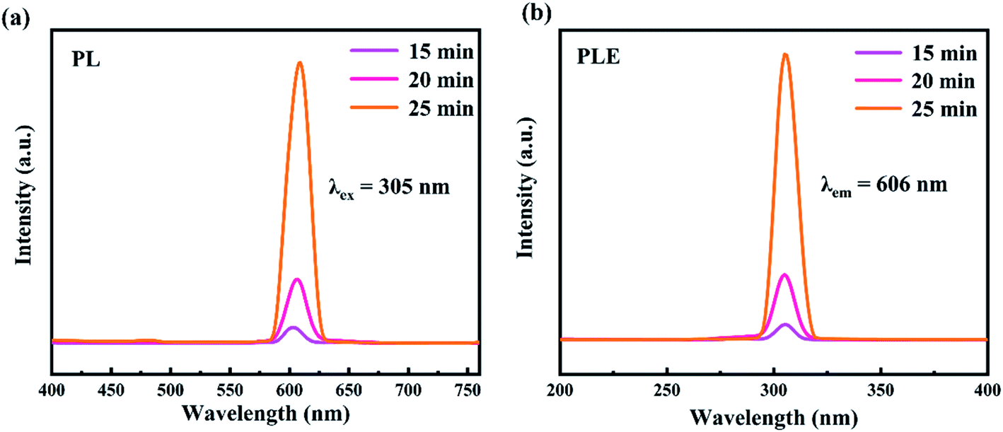 | ||
| Fig. 5 Photoluminescence spectra of CsPbI3 NWs (a) PL (λex = 305 nm) and (b) PLE (λem = 606 nm) spectra. Both are researches on CsPbI3 NWs products that have reacted for 15 min, 20 min and 25 min. | ||
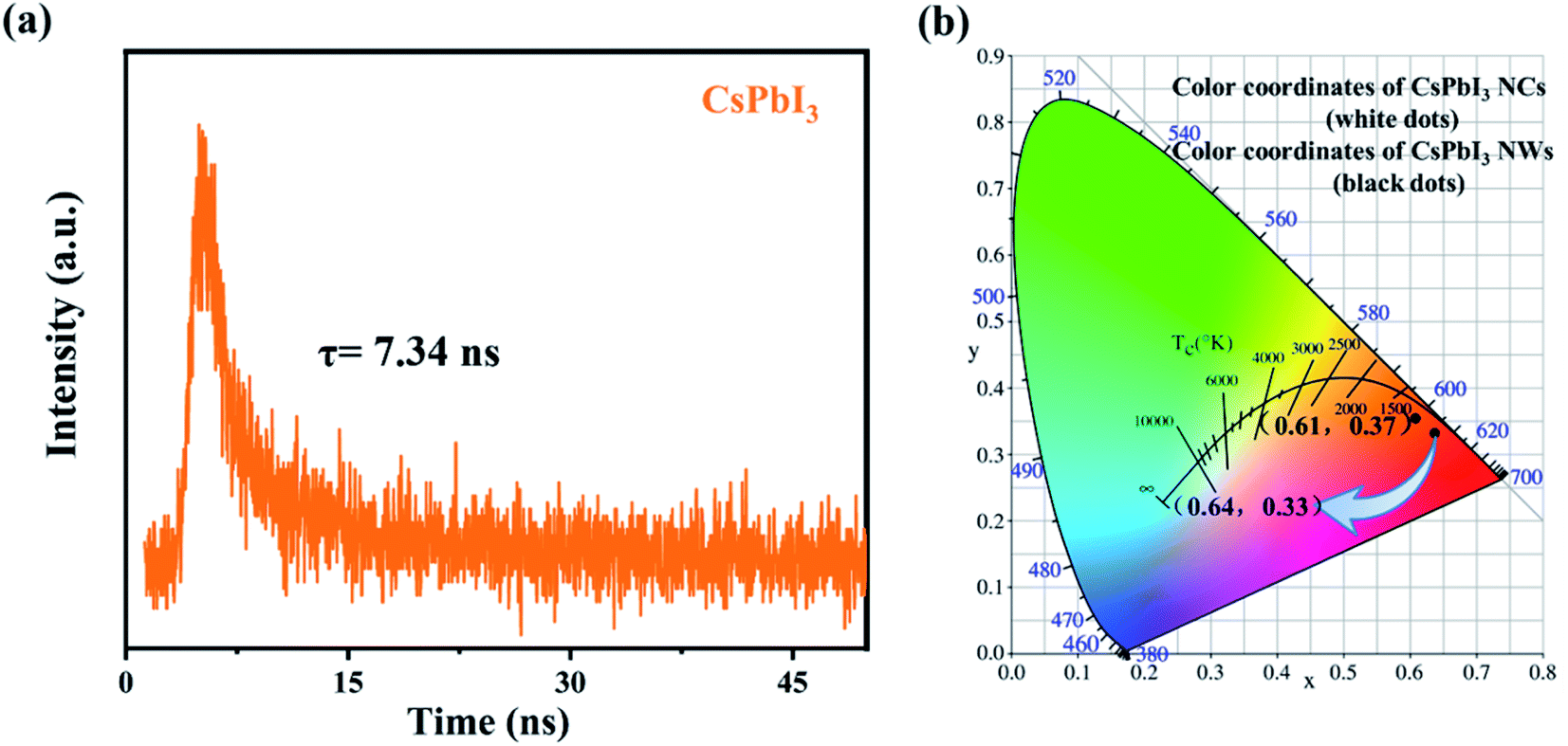 | ||
| Fig. 6 (a) Fluorescence decay curve of CsPbI3 NWs reacted at 155 °C for 15 min. (b) Colour coordinates of CsPbI3 NCs and CsPbI3 NWs. | ||
| Sample | A1 (%) | τ1 (ns) | A2 (%) | τ2 (ns) | tavg (ns) |
|---|---|---|---|---|---|
| CsPbI3 NWs | 52.71 | 1.72 | 11.64 | 11.24 | 7.34 |
Fig. 6(b) shows the chromaticity coordinates of CsPbI3 nanocubes (NCs) and CsPbI3 NWs under excitation at a wavelength of 305 nm. The colour coordinates of CsPbI3 nanocubes (NCs) and NWs are (0.61, 0.37) and (0.64, 0.33), respectively. The coordinate values gradually red-shifted with the increase in time, which correspond to the PL spectrum at the same time. Moreover, we did a stability test on the CsPbI3 NWs. It was found that the experimentally synthesized CsPbI3 NWs may exhibit fluorescence decay phenomenon under UV irradiation (Fig. S3a†). Next, we performed modified experiments on the synthesized CsPbI3 NWs. The same fluorescence test showed a negligible fluorescence intensity change of the NWs (Fig. S3b†), suggesting that the stability can still be improved through modified experiments. The results further proved that the experimental synthesis steps are simple and effective. The study will be continued to further improve the stability of CsPbI3 NWs.
3. Conclusion
In summary, we have developed a novel and facile synthesis strategy for all-inorganic CsPbI3 NWs, of which no inert gas protection during the entire process is required. Also, the synthesis strategy was optimized with reduced reaction steps, time, cost and temperature without the need of catalysts. From the material characterization, the as-synthesized CsPbI3 NWs were crystallized as a single crystal in an orthogonal phase that was arranged orderly with an uniform growth direction. The nanocrystals underwent phase transition from a cubic phase to an orthorhombic phase in a short time during the reaction process and finally remained in the orthorhombic phase. In addition, the CsPbI3 NWs showed a photoluminescence peak at 610 nm and the fluorescence lifetime was 7.34 ns. To summarize, the synthesis strategy reported here simplifies the traditional synthesis method and opens up a new synthesis route for applications in the fields of optoelectronics, semiconductor devices and fluorescent anticorrosion.4. Experimental section
4.1 Materials
Cesium carbonate (Cs2CO3, 99.99%), 1-octadecene (ODE, >90%, GC), lead iodide (PbI2, 99.9%), oleylamine (OAm, 80–90%), and oleic acid (OA, AR), n-hexane (>99%, GC). All chemicals were purchased from Aladdin and used as received without further purification.4.2 Synthesis of CsPbI3 NWs
PbI2 (1.392 g), ODE (80 mL), OAm (8.8 mL), and OA (16 mL) were added into a 250 mL three-neck flask and stirred at 120 °C for 1 h to completely dissolve PbI2. The temperature was then raised to 155–160 °C, and then 2.4 mL of the pre-prepared and preheated Cs-OA solution was quickly injected into the PbI2 solution. After stirring for 15–25 min, the reaction mixture with the synthesized CsPbI3 NWs was cooled in an ice-water bath for the purification process.4.3 Isolation and purification of CsPbI3 NWs
A centrifugation process was performed at 6000 rpm for 5 min to separate the CsPbI3 NWs from the crude solution. After discarding the supernatant, hexane was added to dissolve the precipitate. The centrifugation process was repeated several times to obtain the purified final product of CsPbI3 NWs.4.4 Characterization
Photoluminescence and photoluminescence excitation spectra were recorded at room temperature by Edinburgh FLS1000 with a xenon lamp as the excitation source. Moreover, an Edinburgh steady/transient fluorescence spectrometer FLS1000 was used for testing the decay of PL. Scanning electron microscopy (SEM) images were recorded using a SU8010 (Hitachi Company of Japan) operated at 10 kV. Transmission Electron Microscopy (TEM) images were obtained on a JEOL JEM-F200 electron microscope. Powder X-ray diffraction (XRD) patterns of the obtained products were measured on a PANayltical Empyrean power X-ray diffractometer using monochromatic Cu Kα radiation. The sample powder to be measured was spread on the glass substrate.Author contributions
Kun Nie, Ranran Zhou, and Hua Wang conceived the concept and idea of the present paper, worked on the study design strategy and selected the topics to be discussed. Ranran Zhou completed the main experiment and paper writing, Kun Nie, and Hua Wang were responsible for guidance and supervision work, and at the same time, guided and revised the final paper writing. Chi-An Cheng provided writing assistance and article revisions. Siying Qiu, and Jiayi Chen conducted literature searches, and abstracted the data from the eligible full text articles. Mengyun Wu, and Panlong Lin provided experimental guidance and experimental tests. Luoxin Wang, and Lefu Mei supervised the study. All of the authors discussed the results and commented on the manuscript.Conflicts of interest
The authors declare no competing financial interest.Acknowledgements
This research is supported by the National Natural Science Foundation of China (51672257, 51872269), the Open Project Program of High-Tech and National Project Cultivation Plan of Wuhan Textile University that are greatly acknowledged.Notes and references
- H. Wang, H. Li, W. Cai, P. Zhang, S. Cao, Z. Chen and Z. Zang, Nanoscale, 2020, 12, 14369–14404 RSC.
- J. Burschka, N. Pellet, S. J. Moon, R. Humphry-Baker, P. Gao, M. K. Nazeeruddin and M. Gratzel, Nature, 2013, 499, 316–319 CrossRef CAS PubMed.
- M. Liu, M. B. Johnston and H. J. Snaith, Nature, 2013, 501, 395–398 CrossRef CAS.
- H. Tsai, W. Nie, J. C. Blancon, C. C. Stoumpos, R. Asadpour, B. Harutyunyan, A. J. Neukirch, R. Verduzco, J. J. Crochet, S. Tretiak, L. Pedesseau, J. Even, M. A. Alam, G. Gupta, J. Lou, P. M. Ajayan, M. J. Bedzyk and M. G. Kanatzidis, Nature, 2016, 536, 312–316 CrossRef CAS PubMed.
- H. Guan, S. Zhao, H. Wang, D. Yan, M. Wang and Z. Zang, Nano Energy, 2020, 67, 104279 CrossRef CAS.
- Z. K. Tan, R. S. Moghaddam, M. L. Lai, P. Docampo, R. Higler, F. Deschler, M. Price, A. Sadhanala, L. M. Pazos, D. Credgington, F. Hanusch, T. Bein, H. J. Snaith and R. H. Friend, Nat. Nanotechnol., 2014, 9, 687–692 CrossRef CAS PubMed.
- M. Yuan, L. N. Quan, R. Comin, G. Walters, R. Sabatini, O. Voznyy, S. Hoogland, Y. Zhao, E. M. Beauregard, P. Kanjanaboos, Z. Lu, D. H. Kim and E. H. Sargent, Nat. Nanotechnol., 2016, 11, 872–877 CrossRef CAS PubMed.
- X. Huang, Q. Sun and B. Devakumar, J. Lumin., 2020, 225, 117373 CrossRef CAS.
- H. Wang, P. Zhang and Z. Zang, Appl. Phys. Lett., 2020, 116, 162103 CrossRef CAS.
- L. Dou, Y. M. Yang, J. You, Z. Hong, W. H. Chang, G. Li and Y. Yang, Nat. Commun., 2014, 5, 5404 CrossRef CAS PubMed.
- Z. L. Wang and J. Song, Science, 2006, 312, 242–246 CrossRef CAS PubMed.
- H. Li, W. Lin, L. Ma, Y. Liu, Y. Wang, A. Li, X. Jin and L. Xiong, RSC Adv., 2021, 11, 11663–11671 RSC.
- W. Zhai, J. Lin, C. Li, S. Hu, Y. Huang, C. Yu, Z. Wen, Z. Liu, Y. Fang and C. Tang, Nanoscale, 2018, 10, 21451–21458 RSC.
- Z. Hu, Z. Liu, Z. Zhan, T. Shi, J. Du, X. Tang and Y. Leng, Adv. Photonics, 2021, 3, 034002 CAS.
- G. Xing, N. Mathews, S. S. Lim, N. Yantara, X. Liu, D. Sabba, M. Gratzel, S. Mhaisalkar and T. C. Sum, Nat. Mater., 2014, 13, 476–480 CrossRef CAS.
- H. Zhu, Y. Fu, F. Meng, X. Wu, Z. Gong, Q. Ding, M. V. Gustafsson, M. T. Trinh, S. Jin and X. Y. Zhu, Nat. Mater., 2015, 14, 636–642 CrossRef CAS PubMed.
- X. Tang, Z. Hu, W. Yuan, W. Hu, H. Shao, D. Han, J. Zheng, J. Hao, Z. Zang, J. Du, Y. Leng, L. Fang and M. Zhou, Adv. Opt. Mater., 2017, 5, 1600788 CrossRef.
- X. Bao, M. Li, J. Zhao and Z. Xia, J. Mater. Chem. C, 2020, 8, 12302–12307 RSC.
- Y. Tang, A. Lesage and P. Schall, J. Mater. Chem. C, 2020, 8, 17139–17156 RSC.
- L. Protesescu, S. Yakunin, M. I. Bodnarchuk, F. Krieg, R. Caputo, C. H. Hendon, R. X Yang, A. Walsh and M. V. Kovalenko, Nano Lett., 2015, 15, 3692–3696 CrossRef CAS PubMed.
- S. Zhao, Y. Zhang and Z. Zang, Chem. Commun., 2020, 56, 5811–5814 RSC.
- D. Yan, T. Shi, Z. Zang, T. Zhou, Z. Liu, Z. Zhang, J. Du, Y. Leng and X. Tang, Small, 2019, 1901173 CrossRef PubMed.
- S. Sun, D. Yuan, Y. Xu, A. Wang and Z. Deng, ACS Nano, 2016, 10, 3648–3657 CrossRef CAS PubMed.
- A. Swarnkar, R. Chulliyil, V. K. Ravi, M. Irfanullah, A. Chowdhury and A. Nag, Angew. Chem., Int. Ed., 2015, 54, 15424–15428 CrossRef CAS PubMed.
- S. W. Eaton, M. Lai, N. A. Gibson, A. B. Wong, L. Dou, J. Ma, L. W. Wang, S. R. Leone and P. Yang, Proc. Natl. Acad. Sci. U. S. A., 2016, 113, 1993–1998 CrossRef CAS PubMed.
- Y. Luo, T. Tan, S. Wang, R. Pang, L. Jiang, D. Li, J. Feng, H. Zhang, S. Zhang and C. Li, Nanoscale, 2021, 13, 4899–4910 RSC.
- Y. Li, H. Zhang, P. Liu, Y. Wang, H. Yang, Y. Li and H. Zhao, Electrochem. Commun., 2015, 51, 6–10 CrossRef.
- D. Zhang, S. W. Eaton, Y. Yu, L. Dou and P. Yang, J. Am. Chem. Soc., 2015, 137, 9230–9233 CrossRef CAS PubMed.
- K. Nie, Q. An and Y. Zhang, Nanoscale, 2016, 8, 8791–8797 RSC.
- Y. Bekenstein, B. A. Koscher, S. W. Eaton, P. Yang and A. P. Alivisatos, J. Am. Chem. Soc., 2015, 137, 16008–16011 CrossRef CAS.
- T. Udayabhaskararao, M. Kazes, L. Houben, H. Lin and D. Oron, Chem. Mater., 2017, 29, 1302–1308 CrossRef CAS.
- B. A. Koscher, J. K. Swabeck, N. D. Bronstein and A. P. Alivisatos, J. Am. Chem. Soc., 2017, 139, 6566–6569 CrossRef CAS PubMed.
- J. A. Steele, H. Jin, I. Dovgaliuk, R. F. Berger, T. Braeckevelt, H. Yuan, C. Martin, E. Solano, K. Lejaeghere, S. M. J. Rogge, C. Notebaert, W. Vandezande, K. P. F. Janssen, B. Goderis, E. Debroye, Y.-K. Wang, Y. Dong, D. Ma, M. Saidaminov, H. Tan, Z. Lu, V. Dyadkin, D. Chernyshov, V. Van Speybroeck, E. H. Sargent, J. Hofkens and M. B. J. Roeffaers, Science, 2019, 365, 679–684 CrossRef CAS PubMed.
- D. M. Trots and S. V. Myagkota, J. Phys. Chem. Solids, 2008, 69, 2520–2526 CrossRef CAS.
- X. Tang, X. Hou, D. Shu and P. Zhai, Sci. China: Technol. Sci., 2015, 58, 1712–1716 CrossRef CAS.
- Y. L. Lai, C.-P. Liu and Z.-Q. Chen, Appl. Phys. Lett., 2005, 86, 121915 CrossRef.
- H. Huang, M. I. Bodnarchuk, S. V. Kershaw, M. V. Kovalenko and A. L. Rogach, ACS Energy Lett., 2017, 2, 2071–2083 CrossRef CAS PubMed.
- J. M. Ball and A. Petrozza, Nat. Energy, 2016, 1, 16149 CrossRef CAS.
- X. Shen, S. Wang, C. Geng, L. Li, E. Zhao, J. Sun, W. Wu, L. An and K. Pan, J. Phys. Chem. C, 2021, 125, 5278–5287 CrossRef CAS.
- D. Chen, Y. Liu, C. Yang, J. Zhong, S. Zhou, J. Chen and H. Huang, Nanoscale, 2019, 11, 17216–17221 RSC.
- P. Li, W. Xie, W. Mao, Y. Tian, F. Huang, S. Xu and J. Zhang, J. Alloys Compd., 2020, 817, 153338 CrossRef CAS.
- X. Bao, M. Li, J. Zhao and Z. Xia, J. Mater. Chem. C, 2020, 8, 12302–12307 RSC.
Footnote |
| † Electronic supplementary information (ESI) available. See DOI: 10.1039/d1ra04429j |
| This journal is © The Royal Society of Chemistry 2021 |