
 Open Access Article
 This Open Access Article is licensed under a Creative Commons Attribution-Non Commercial 3.0 Unported Licence
Single wall carbon nanotube based optical rectenna
Lina Tizani ac,
Yawar Abbasb,
Ahmed Mahdy Yassinac,
Baker Mohammadac and
Moh’d Rezeq*bc
ac,
Yawar Abbasb,
Ahmed Mahdy Yassinac,
Baker Mohammadac and
Moh’d Rezeq*bc
aDepartment of Electrical Engineering and Computer Science, Khalifa University, Abu Dhabi, 127788, UAE
bDepartment of Physics, Khalifa University, Abu Dhabi, 127788, UAE. E-mail: mohd.rezeq@ku.ac.ae
cSystem on Chip Center, Khalifa University, Abu Dhabi, 127788, UAE
First published on 8th July 2021
Abstract
We present an optical rectenna by engineering a rectifying diode at the interface between a metal probe of an atomic force microscope (AFM) and a single wall carbon nanotube (SWCNT) that acts as a nano-antenna. Individual SWCNT electrical and optical characteristics have been investigated using a conductive AFM nano-probe in contact with two device structures, one with a SWCNT placed on a CuO/Cu substrate and the other one with a SWCNT on a SiO2/Si substrate. The I–V measurements performed for both designs have exhibited an explicit rectification behavior and the sensitivity of carbon nanotube (CNT)-based rectenna to light. The measured output current at a set voltage value demonstrates the significant effect of the light irradiation on the current signal generated between the Au nano-probe and CNT interface. This effect is more prominent in the case of the CuO/Cu substrate. Detailed analysis of the system, including the energy band diagram, materials characterization and finite element simulation, is included to explain the experimental observations. This work will pave the way for more investigations and potential applications of CNTs as nano-rectennas in optical communication and energy harvesting systems.
Introduction
Optical antennas represent an optical detector similar to radio-frequency antennas but operating in the optical regime. Nowadays, optical antennas are attracting a lot of attention due to their potential for wide applications in nano-scale optical microscopy, spectroscopy, solar energy conversion, integrated optical nano-circuitry, molecular sensing, etc.1 This increased focus on nano-antennas is due to the progress in nano-manufacturing technologies, which makes it possible to utilize sub-wavelength plasmonic structures in different shapes and sizes.2 One essential synthesis process required for the realization of nano-antennas at a small scale (nano scale) is utilizing a nano-probe that relies on ultra-sharp tips3,4 in making physical contact with individual CNTs. Moreover, this has been integrated with a new approach used for modeling and fabrication of a tunneling-based nano-Schottky diode rectifier.5CNTs' outstanding electrical, mechanical, and physical properties make them ideal candidates for many potential applications including transistors,6–8 gas sensors,9,10 optical sensors,11 light emitters12,13 and for MEMS/NEMS applications.14 Also, CNTs make exemplary antenna elements as they absorb electromagnetic energy in a broad spectrum.15,16 Since the 1D growth technique is rapidly developing, CNTs will not only substitute materials in many areas, but also will introduce new devices with improved performances. The nano-scale size will introduce unique properties for CNT-based photo-detectors that can reduce dark current due to the small size of CNTs.17 In addition, the high surface to volume ratio of the CNT can improve the sensitivity of the photo-detectors. More interestingly, in addition to their high conductivity single wall carbon nanotubes (SWCNTs) which can be obtained by geometrically rolling a graphene sheet, have showed a band gap structure with a band gap that varies from 0 to 2 eV.18 Several major techniques have been used to synthesize CNT's: arc discharge, laser ablation, and chemical vapor deposition (CVD).19
Classical rectenna is formed from an antenna and a diode connected. The rectenna at optical frequency encounter several fundamental challenges related to the rectifier operating at high frequency as well as the antenna having a low RC time constant. Several types of diodes have been explored Metal/Insulator/Metal (MIM) and Metal/Insulator/Insulator/Metal (MIIM) diodes, diodes that combine multiple dielectrics show better performance than single insulator diodes through more control of electron tunneling.20 A new approach has been demonstrated using CNT in the rectenna design. This has been demonstrated and fabricated for the first time using multi wall CNT vertically aligned as metal electrode in MIM diode. These rectenna devices show increased nonlinearity when illuminated.21 Another rectenna using multi insulator along with CNT as metal electrode has been fabricated and used in order to model the photon assisted tunneling mechanism. This rectenna shows excellent rectification behavior in the optical regime.22
In this work, we have investigated the opto-electrical behavior of SWCNTs as nano-rectennas. However, isolating an individual carbon nanotube is an essential requirement for testing light detection characteristics of SWCNT-based nano-rectenna. Pristine CNTs as synthesized are bundled. They are hard to disperse due to the strong van der Waals forces and their high aspect ratios. Various solvents have been reported to successfully debundle CNTs as well as obtaining stable and dispersed nanotubes.4,23–33 N-Methylpyrrolidone (NMP) has been a highly effective solvent for dispersing and debundling SWCNTs.23–26
Here we show that an efficient optical rectenna can be constructed by using individually dispersed SWCNT on metal oxide or silicon oxide substrates. The optical characteristics of rectenna are demonstrated using conductive mode atomic force microscope (C-AFM). This demonstration is based on the field enhancement at the carbon nanotube interface with the metal nano-probe of C-AFM. Using C-AFM equipped with a white light source, we measured the electrical characteristics of the nano-diode and the effect of the adsorption of the optical light by the CNT. The results agree with the rectenna theory21,34 where our devices show a clear field rectification from the antenna.
Experimental measurements
Dispersing single wall CNTs (SWCNTs)
Materials used in this experiment: SWCNTs powder with the chirality (7,6), ≥77% carbon as SWCNT and 2–3 nm diameter in average from Sigma-Aldrich. N-Methyl-2-pyrrolidone (NMP) used for dispersion of these SWCNTs from the powder. 1.0 mg of SWCNT powder was mixed with 15 ml of NMP, the resulting mixture of SWCNT was tip sonicated for 2.0 minutes. This initial dispersion was serially diluted in order to produce a range of solutions with different concentrations from 0.066 mg ml−1 to 0.0093 mg ml−1. After each dilution, the solution was sonicated by tip for 2.0 minutes. The resulting mixture was bath sonicated for 4 h followed by 1 minute tip sonication. This sonication process is considered the most essential step in the dispersion process where most nanotubes de-bundle.33 A small volume was drop-casted on a clean substrate at room temperature and dried in a vacuum oven at 120 °C for 4 hours as shown Fig. 1(a). The substrate was cleaned using a bath sonication in acetone followed by isopropanol and distilled water. Two substrates were used in our experiments: the first substrate is n-Si with 2.31 nm SiO2 layer on the top. Fig. 1(b) shows the schematic of SiO2/n-Si substrate and the thickness of SiO2 was measured using spectroscopic ellipsometry. The second substrate is a copper sheet with a thickness of 625 μm. The substrate is cleaned using a bath sonication in acetone followed by isopropanol and distilled water. Oxidation at temperatures lower than 400 °C leads to the growth of a thin copper oxide layer (CuO) over the Cu surface.35 For our device, a thin layer of copper oxide of 3.69 nm, measured by spectroscopic ellipsometry, is formed by thermal oxidation of Cu by heating at 150 °C for 1 h prior to the deposition of CNT, as shown Fig. 1c. In our work, the concentration of 0.0093 mg ml−1 of SWCNTs was used to prepare our samples, since no aggregates have been reported to be present below 0.02 mg ml−1 that is considered as nanotube dispersion limit in NMP.26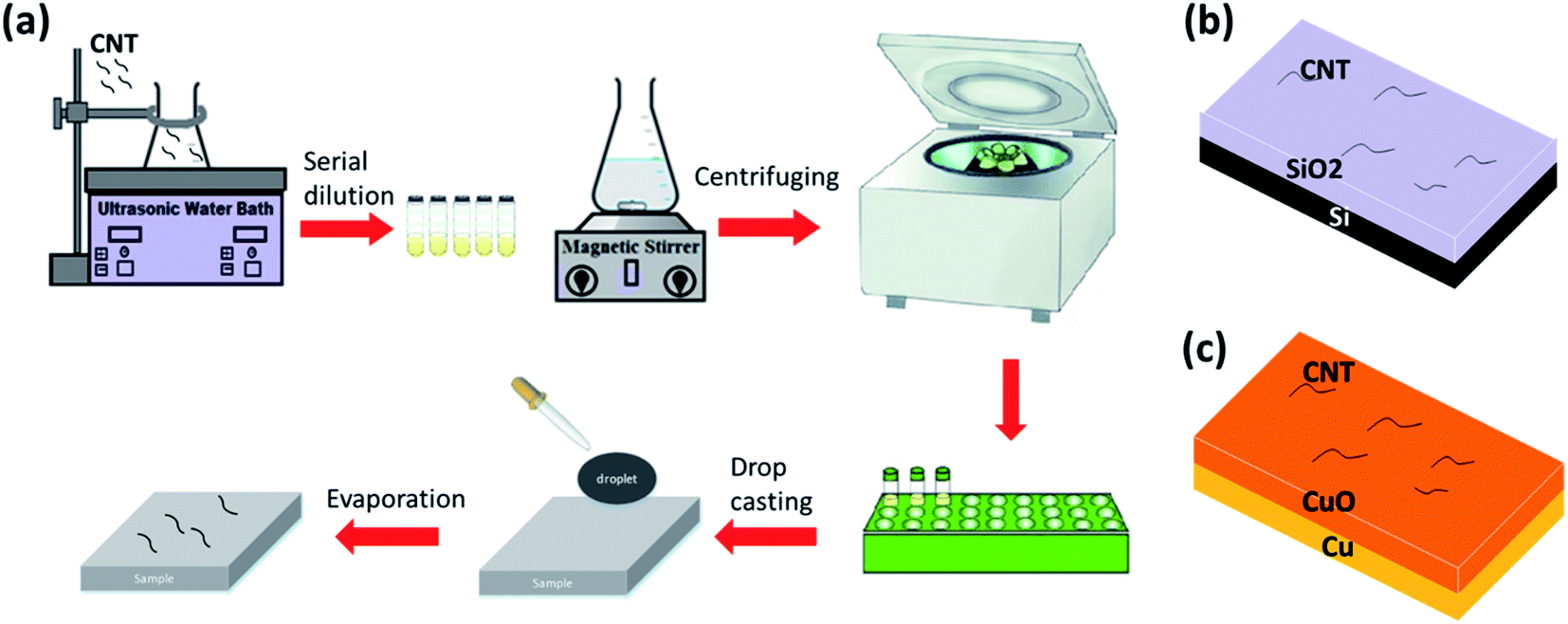 | ||
| Fig. 1 (a) Steps for the dispersion of CNT powder and sample preparation, (b) schematic of the first device using Si as a substrate with a thin SiO2 layer of 2.31 nm, (c) schematic of the second device using Cu sheet as the substrate with a thin CuO layer of 3.69 nm. | ||
Measurement methodology and CNT characterization
Conductive mode atomic force microscope (C-AFM) has been used as a powerful tool to investigate the photo detection and rectification behavior at the nano-scale metal-semiconductor (MS) junctions.36–39 Using C-AFM we can determine the topography and the electrical properties simultaneously with the help of a conductive tip, while a bias voltage is applied on the sample and the tip is kept at ground as shown in Fig. 2(a). During the acquisition of the I–V curves, the tip is brought into contact with the CNT of interest. To assess the light and dark condition of CNT nano-rectenna, the I–V measurements were performed using the AFM system that is placed in a closed chamber by switching the light source on and off with 0.1 Hz (10 s), which is guided via and optical fiber to the junction between the probe and the sample. In our experiment, the light source is broadband, halogen dimming light source with a power of 50 W and a wavelength spectrum between 500 nm and 1000 nm, with more intensity concentrated between 650 nm and 950 nm. The highest power is observed at 730 nm. We have tested two structures of CNT-based rectennas using Au AFM tip, for performance comparison and optimization. In one design, the SWCNTs are dispersed on SiO2/Si substrate, and in the second structure the SWCNTs is dispersed on CuO/Cu substrate, as shown in Fig. 1(b) and (c) respectively. A scanning electron microscope (SEM) imaging of the tip has been performed, Fig. 2(b), and Energy Dispersive X-ray analysis (EDX) to confirm the sharpness and the conductive material of the tip. The topography and material of the CNT has also been explored in tapping mode AFM, Fig. 2(c), SEM, Fig. 2(d) and TEM, Fig. 2(f), showing the diameter of CNT is 3.5 nm. Raman spectroscopy of SWCNT shown in Fig. 2(e) shows a well defined G (1586.11 cm−1) and G′ (2634.56 cm−1) peak with a high intensity for the G peak which confirms that the material is a SWCNT with a fewer defect determined by the intensity of D peak (1327.31 cm−1).40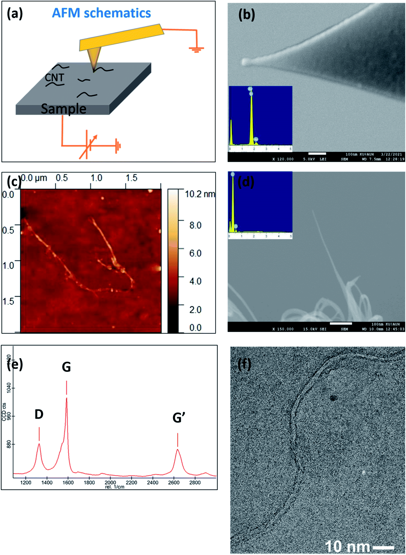 | ||
| Fig. 2 (a) The schematic illustration of the electrical measurement carried out by conductive atomic force microscope, (b) SEM image of the Au tip of 37 nm radius, inset EDX showing the conductive material of the nano probe, (c) AFM topography of single carbon nanotube on top of SiO2/Si substrate, (d) SEM image of SWCNT with approximate diameter of 2–3 nm, inset EDX showing carbon element in the single wall carbon nanotubes, (e) Raman spectra for a SWCNT showing D band, G band and G′ band at 1327.31 cm−1, 1586.11 cm−1 and 2634.56 cm−1 respectively, (f) TEM image of SWCNT. | ||
For further characterization of the shape of SWCNTs, AFM topographical images of several samples revealed that the average diameter of the nanotube after dispersion is approximately 3 nm, Fig. 3, which corresponds to an energy band gap of 0.246 eV.41
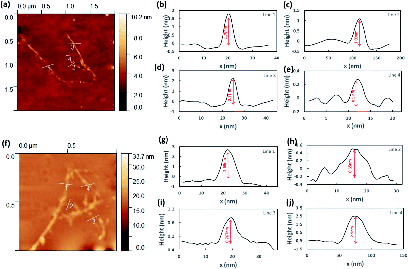 | ||
| Fig. 3 (a) AFM topography image and the corresponding diameter distribution along: (b) line 1, (c) line 2, (d) line 3, (e) line 4, (f) AFM topography image and the corresponding diameter distribution along: (g) line 1, (h) line 2, (i) line 3, (j) line 4. The average diameter of SWCNT is 2.2 nm. | ||
Results and discussion
Photoelectric response of CNT devices
To assess the response and reproducibility of the CNT-based rectifier, measurements have been repeated on several samples and on random single CNTs chosen at the surface of both substrates. Due to the nanometer size of the tip, the I–V curves reflect the effect of the electric field enhancement at the nano-tip/CNT interface as well as the light effect on this junction. A voltage sweep between −1.0 V to 1.0 V is applied on the substrate while the AFM gold coated tip is grounded. The I–V characteristics of Au–CNT–SiO2–Si and Au–CNT–CuO–Cu structures with and without white light illumination have been measured as shown in Fig. 4(a) and (b) respectively. The effect of light illumination without a deposited CNT on the surface of the substrate has also been explored using the same bias condition. To confirm the repeatability of the electrical characteristics, the measurements have been repeated several times and at the same voltage sweeps with and without light illumination. For the first sample with CNTs on SiO2, Fig. 4(a), the I–V curves show clearly the diode rectification behavior with a high current in the forward (negative bias) after a turning-on voltage around (−0.65 V). However, after switching the light on the forward current increased significantly at a lower turning-on voltage (−0.5 V). These measurements have been repeated several times with the light on and off, as shown in the overlapping curves in Fig. 4(a). Moreover, the current has been measured at a fixed applied voltage in the forward bias, namely −1.0 V, when the probe is placed on the CNT/SiO2/Si stack and while the light is turned on/off for 10 seconds. The light effect is evident from the rectangular profile in Fig. 4(c), where a higher current is measured for 10 s when the light is on versus a negligible current when light is off. To confirm the rectification behavior of CNTs and their sensitivity to the light, the same measurements where performed on the second sample of SWCNTs placed on a CuO/Cu substrate, as in Fig. 4(b). The I–V data when the light is off showed the current increases rapidly after a turn-on voltage in the forward bias around −0.15 V (solid black line). In the reverse bias situation, electron tunneling occurs through the oxide layer at around 0.26 V. Interestingly, when the light is on (red line), the turn-on voltage decreases to around −0.10 V, and the current increase even faster afterward. In the reverse bias the tunneling current is not affected by the light, and the curves overlap when the light is on and off. For further confirmation, the probe was placed on the CuO surfaces where there is no CNTs. The I–V data, as shown with a blue curve in Fig. 4(b), exhibits a very small current in the forward bias and a tunneling current in the reverse bias at a relatively higher voltage, higher than ∼0.40 V, and the light has no effect on this I–V curve. The current is also taken at a fixed voltage −0.3 V with light is on and off for 10 seconds and exhibited a prominent effect as shown in Fig. 4(d). | ||
| Fig. 4 (a) Electrical characteristics of Au/CNT/SiO2/Si device and reproducibility of photo detection phenomenon, inset is an AFM topography of single CNT and point of test, (b) electrical characteristics of Au/CNT/CuO/Cu device and reproducibility of photo detection phenomenon, inset is an AFM topography of single CNT at point A; electrical characteristics of Au/CuO/Cu device, test at point B, (c) light response of Au/CNT/SiO2/Si device at a reading voltage value of (−1.0 V), (d) light response of Au/CNT/CuO/Cu device at a reading voltage value of (−0.30 V). | ||
The difference between the current values with and without illumination is evident in devices where the CNT is present in the forward bias condition for the two different devices characterized. The typical on/off current ratio is 38 for CNT on SiO2/Si substrate, at a reading voltage value of (−1.0 V), and 43 for CNT on CuO/Cu substrate at a reading voltage of (−0.30 V). The relatively higher on/off current ratio in the latter case at a much lower voltage (−0.30 V) indicates much higher sensitivity of SWCNT on CuO/Cu substrate. When the devices are illuminated, electrons oscillation is produced inside the antenna. This oscillation causes a modulation of the Fermi level at the barrier of the diode. Similarly to photon assisted tunneling (PAT) in rectennas based on multi-wall CNT,22 an electron absorbs or emits a certain number of photons and this will be reflected as a shift in the (I–V) curve.
To investigate the antenna's behavior of SWCNT, we have also tested the light effect on devices with different CNT lengths by reading the light current I (light) at a given voltage value of (−1.0 V), as a feasible approach. For short length device with CNT length L = 0.4 μm, a relatively high current I (light) is measured. The 0.4 μm length of CNT antenna corresponds to a wavelength of light of approximately 800 nm. As mentioned previously, the halogen source used in our experiment has a spectrum with the highest power intensity between 650 nm and 900 nm. Thus for our measurements the 0.4 μm CNT length antenna is correlated to the highest intensity of the light which explains the highest current measured at this value. This light current decreases with increasing the length of the CNT, as shown in Fig. 5, which indicates the direct dependence of the light absorption on the SWCNT antennas dimensions. The variation in photocurrent is totally antenna effect that depends on the wavelength as in optical antennas. When the light interacts with optical antennas with specific dimensions, surface plasmons are generated and only at resonant frequency, light will be absorbed and irradiated.42 This dependence of the device current on the length of the CNT provide potential design opportunities for antennas at a different wavelength. Moreover, for our source, the photon energy lies in the range 1.24 eV and 2.48 eV. This means that some effect from the photon tunneling have also contributed to the response of our device. For this reason, the behavior is a combination of both drift and tunneling currents.
 | ||
| Fig. 5 Variation of the light current at a reading voltage of (−1 V) for Au/CNT/SiO2/Si device as a function of CNT length extracted from AFM topography images. | ||
Data analysis and physical models
The properties of the Schottky barrier, including barrier height and depletion width are determined by the energy level alignment of the metal and CNT. Understanding the CNT Schottky barrier based on the energy band diagram can guide to an optimized CNT rectenna design. The measured I–V characteristics of SWCNT on both metal oxide and semiconductor oxide samples can be readily understood by visualizing these interfaces' energy band diagram structures. We start with the case of SWCNT placed on CuO/Cu substrate. At the beginning, we analyze the energy band structure when the gold nano-probe is placed on the surface without CNTs. Fig. 6(a) shows the energy band diagram of Au, CuO and Cu just before the physical contact and during the contact case at zero bias. At thermal equilibrium, the Fermi levels in the stack of materials (Au/CuO/Cu) are aligned. When a positive bias is applied on the Cu substrate, the current was negligible until a threshold voltage was reached. Here the conduction band of CuO is brought at a lower level than the Au Fermi level. Due to the enhancement of the electric field at the nano-probe, the electric field on the probe is quite relatively high at this threshold voltage. This results in a thin tunneling barrier,43 which allows electrons to tunnel through the CuO into Cu bulk, as shown the Fig. 6(b) and evident in the experimental data in Fig. 4(b) (blue line) at an applied voltage around 0.40 V. However, when the applied voltage polarity is reversed an additional applied voltage is needed to overcome the built-in potential due to Fermi levels alignment between Au/CuO/Cu interfaces as in shown in Fig. 6(a), in addition to relatively lower electric field on the flat Cu plate, unlike the case when a CNT is present. Therefore, within the same range of the applied voltage sweep the barrier is still thick and blocking electrons to tunnel to the Au nano probe side, as in the schematic in Fig. 6(c). This explains the small current (blue line) in Fig. 4(b) at a negative bias less than −1.0 V. When the Au nano-probe is placed on SWCNT, Fig. 6(d) shows the energy band diagram of Au/CNT/CuO/stack before and after contact. The highly conductive SWCNT with the small diameter size (∼2.0 nm) in addition to the close Fermi levels value between SWCNT and Cu determine the stack electronic structure. At the positive bias the electric field is enhanced due to the small CNT radius, thus narrower tunneling barrier is created (Fig. 6(e)), and the tunneling takes place at a lower threshold voltage as evident in Fig. 4(b) (red curve) at around +0.27 V. On the other hand, when the polarity of the applied voltage is reversed the electron field enhancement at CNT/CuO interface allows the electron to tunnel from Cu bulk into the conduction band of SWCNT. These electrons will in turn continue to flow over the conduction band of CNT and to the Au nano-probe with a lower Fermi level under the forward bias, as in the schematic in Fig. 6(f). This is in accordance with the experimental data in Fig. 4(b) (black curve) at negative bias, around −0.15 V. When the light is shed on the sample, CNT tubes whose length lies within the range of the optical light spectrum would resonate with the light waves. More energetic electrons will flow over the conduction band to the Au nano-probe, hence more current at a relatively lower threshold voltage (−0.10 V) will be observed. This photo effect is only observed in the forward (negative bias) as electrons can move easier over to the conduction band to the lower Fermi level of Au nano-probe. | ||
| Fig. 6 Schematics of the energy band diagrams for CuO/Cu sample. The Fermi level is denoted EF, ϕ is the metal work function, Ec and Ev is the conduction and valence band respectively and Ea electron affinity. (a), (b), and (c) correspond to Au/CuO/Cu stack after contact, in reverse bias and forward bias respectively. The upper blue dotted lines show CuO conduction band and Cu Fermi level before contact. (d), (e) and (f) correspond to Au/CNT/CuO/Cu device stack after contact, at 0 bias, in reverse bias, and forward bias respectively. | ||
For further analysis of the electric field at the interfaces, we performed finite element simulation using COMSOL software for both cases, when the Au probe is placed on CuO/Cu and when it is placed directly on CNT/CuO/Cu stack. Fig. 7(a) shows the simulation model of Au nano-probe on CuO/Cu substrate. The electric field distribution and electric field profile at the Au/CuO interfaces are shown in Fig. 7(b) and (c), respectively. Fig. 7(c) shows the maximum field at Au/CuO interface at different voltages. For instance, at a threshold voltage 0.40 V, as in Fig. 4(b), the interface maximum electric field is around 1.2 × 10⁸ V m−1, which is high enough for electron tunneling through CuO thin layer. Fig. 7(d), (e), and (f) show the simulation model, electric field distribution and electric field profile respectively for Au/CNT/CuO/Cu stack. Fig. 7(f) shows the electric field profiles, at the interface between CNT/CuO, at different applied voltages. We can readily see that a similar electric field (∼1.2 × 10⁸ V m−1) is obtained at a voltage around ∼0.26 V, which is consistent with the threshold tunneling voltage in Fig. 4(b), in CNT/CuO case. This explains the lower threshold voltage in the reverse (positive) bias in Fig. 4(b), when the probe is placed directly on the CNT.
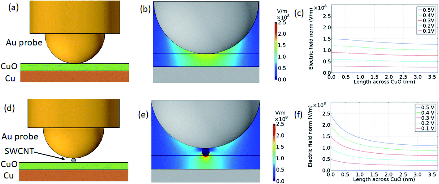 | ||
| Fig. 7 (a) COMSOL simulation model for Au probe on CuO/Cu sample. (b) The electric field distribution at the interface. (c) The electric field profile along a vertical middle line a cross CuO layer, at different applied voltages. (d) COMSOL simulation model for Au probe on CNT/CuO/Cu sample. (e) The electric field distribution at the interface. (f) The electric field profile along a vertical middle line a cross CuO layer, at different applied voltages. | ||
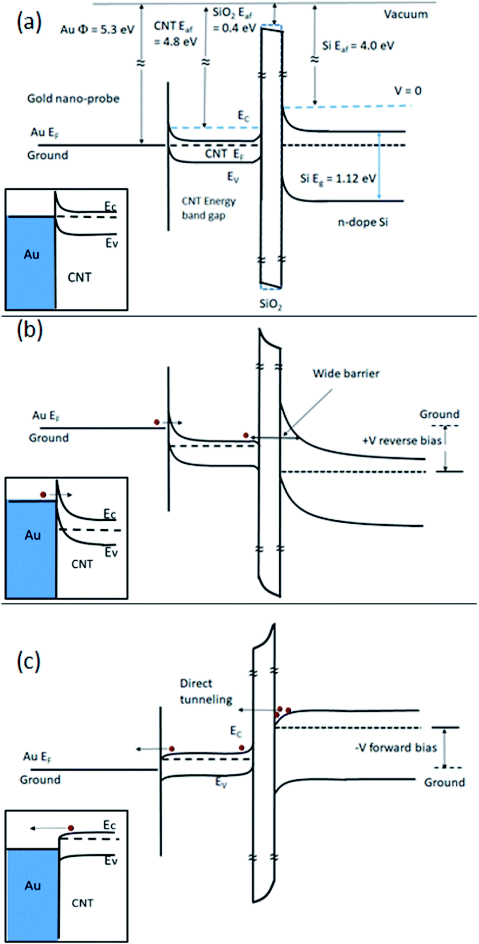
For the other device structure, when SWCNTs are dispersed on SiO2, the energy band diagram for Au/CNT/SiO2/Si is shown in the schematic in Fig. 8(a), before and after contact. When a positive voltage is applied on the Si substrate this shifts the conductions bands of Si, SiO2 and CNT down, as shown in Fig. 8(b). Although the tunneling barrier at Au/CNT interface is thin electrons at CNT conduction band encounter a much wider barrier at CNT/SiO2/Si interface due to depletion region in Si bulk, as shown in the schematic in Fig. 8(b). This explains the minimal current in the reverse bias, as in experimental data in Fig. 4(a) (red curve). On the other hand, in the forward bias (negative applied voltage), as shown in the schematic in Fig. 8(c), the conduction band of Si is lifted up, and electrons can undergo direct tunneling through the very thin (∼2.0 nm) SiO2 layer44,45 to the conduction band of CNT, and then electrons will drift smoothly to the lower Au Fermi level in the nano-probe, Fig. 8(c). This is evident from the experimental data in Fig. 4(a) (red curve). When the light is shed on the sample and optical EM waves are absorbed by the CNT more energetic electrons will flow over the conduction band of the SWCNT to the probe, and thus more current is observed as in Fig. 4(a) (red curve). However, in the reverse bias electrons will encounter a wide barrier at CNT/SiO2/Si junction (50–200 nm), therefore, the light effect is not observed.
 | ||
| Fig. 8 Schematics of the energy band diagram of Au/CNT/SiO2/Si. (a) At zero bias. (b) Reverse (positive) bias. (c) Forward (negative) bias. With inset showing a simplified nano Schottky junction between Au and CNT. | ||
Conclusion
In conclusion, we have investigated the electrical characteristics of single wall carbon nanotubes (SWCNTs) and their response to the optical light towards developing CNTs based nano rectenna devices. Two types of device structures have been explored by dispersing CNTs on CuO/Cu substrate and the other by dispersing SWCNTs on SiO2/Si. The measurements data showed a clear and sensitive response of SWCNT to light by placing the probe directly on the CNT. To eliminate the substrate effect, the electrical measurements are carried out directly on the surfaces of SiO2/Si and CuO/Cu and no light impact is observed. The formation of nano Schottky junction between the CNT and the metal provides a perfect rectification behavior. The response of SWCNTs to light was also found to be dependent on their length. These unique characteristics of SWCNTs present them as a potential candidate for applications in optical communication systems and solar energy harvesting with CuO/Cu as a preferable substrate option for nano-rectenna fabrication.Author contributions
M. Rezeq conceived the idea and supervised the experimental work and paper writing. L. Tizani and Y. Abbas performed the sample preparation, electrical and physical characterization. A. Yassin performed the simulation. L. Tizani performed the manuscript drafting. B. Mohammad contributed to data analysis, manuscript editing, and secured funding. All authors reviewed the manuscript.Conflicts of interest
There are no conflicts to declare.Acknowledgements
This publication is based upon work supported by Khalifa University of Science and Technology under award no. 8474000134.References
- P. Biagioni, J.-S. Huang and B. Hecht, Nanoantennas for visible and infrared radiation, Rep. Prog. Phys., 2012, 75(2), 024402 CrossRef.
- F. B. Zarrabi, M. Naser-Moghadasi, S. Heydari, M. Maleki and A. S. Arezomand, Cross-slot nano-antenna with graphene coat for bio-sensing application, Opt. Commun., 2016, 371, 34–39 CrossRef CAS.
- M. d. Rezeq, A. Ali and H. Barada, Fabrication of nano ion–electron sources and nano-probes by local electron bombardment, Appl. Surf. Sci., 2015, 333, 104–109 CrossRef CAS.
- M. d. Rezeq, Finite element simulation and analytical analysis for nano field emission sources that terminate with a single atom: A new perspective on nanotips, Appl. Surf. Sci., 2011, 258(5), 1750–1755 CrossRef CAS.
- Y. Abbas, A. Rezk, S. Anwer, I. Saadat, A. Nayfeh and M. d. Rezeq, Improved figures of merit of nano-Schottky diode by embedding and characterizing individual gold nanoparticles on n-Si substrates, Nanotechnology, 2020, 31(12), 125708 CrossRef CAS PubMed.
- R. Martel, T. Schmidt, H. Shea, T. Hertel and P. Avouris, Single-and multi-wall carbon nanotube field-effect transistors, Appl. Phys. Lett., 1998, 73(17), 2447–2449 CrossRef CAS.
- A. D. Franklin, The road to carbon nanotube transistors, Nature, 2013, 498(7455), 443–444 CrossRef CAS PubMed.
- A. D. Franklin and Z. Chen, Length scaling of carbon nanotube transistors, Nat. Nanotechnol., 2010, 5(12), 858–862 CrossRef CAS.
- T. Kawno, H. C. Chiamori, M. Suter, Q. Zhou, B. D. Sosnowchik and L. Lin, An electrothermal carbon nanotube gas sensor, Nano Lett., 2007, 7(12), 3686–3690 CrossRef PubMed.
- Z.-D. Lin, S.-J. Young and S.-J. Chang, CO 2 gas sensors based on carbon nanotube thin films using a simple transfer method on flexible substrate, IEEE Sensor. J., 2015, 15(12), 7017–7020 CAS.
- V. Pavelyev, N. Tripathi, P. Mishra, A. Mezhenin, Y. G. Kurenkova and M. Sovetkina, CNT-based IR-sensor, J. Phys.: Conf. Ser., 2018, 1096(1), 012127 CrossRef.
- J. Misewich, R. Martel, P. Avouris, J. Tsang, S. Heinze and J. Tersoff, Electrically induced optical emission from a carbon nanotube FET, Science, 2003, 300(5620), 783–786 CrossRef CAS.
- M. Freitag, et al., Hot carrier electroluminescence from a single carbon nanotube, Nano Lett., 2004, 4(6), 1063–1066 CrossRef CAS.
- X. Zang, Q. Zhou, J. Chang, Y. Liu and L. Lin, Graphene and carbon nanotube (CNT) in MEMS/NEMS applications, Microelectron. Eng., 2015, 132, 192–206 CrossRef CAS.
- X. He, et al., Carbon nanotube terahertz detector, Nano Lett., 2014, 14(7), 3953–3958 CrossRef CAS PubMed.
- S. Kumar, M. Nehra, D. Kedia, N. Dilbaghi, K. Tankeshwar and K.-H. Kim, Carbon nanotubes: A potential material for energy conversion and storage, Prog. Energy Combust. Sci., 2018, 64, 219–253 CrossRef.
- U. Bockelmann and G. Bastard, Phonon scattering and energy relaxation in two-, one-, and zero-dimensional electron gases, Phys. Rev. B, 1990, 42(14), 8947 CrossRef CAS.
- J.-C. Charlier, X. Blase and S. Roche, Electronic and transport properties of nanotubes, Rev. Mod. Phys., 2007, 79(2), 677 CrossRef CAS.
- Y. Ando, X. Zhao, T. Sugai and M. Kumar, Growing carbon nanotubes, Mater. Today, 2004, 7(10), 22–29 CrossRef CAS.
- S. Grover and G. Moddel, Applicability of metal/insulator/metal (MIM) diodes to solar rectennas, IEEE J. Photovolt., 2011, 1(1), 78–83 Search PubMed.
- A. Sharma, V. Singh, T. L. Bougher and B. A. Cola, A carbon nanotube optical rectenna, Nat. Nanotechnol., 2015, 10(12), 1027–1032 CrossRef CAS PubMed.
- E. C. Anderson and B. A. Cola, Photon-assisted tunneling in carbon nanotube optical rectennas: Characterization and modeling, ACS Appl. Electron. Mater., 2019, 1(5), 692–700 CrossRef CAS.
- K. D. Ausman, R. Piner, O. Lourie, R. S. Ruoff and M. Korobov, Organic solvent dispersions of single-walled carbon nanotubes: toward solutions of pristine nanotubes, J. Phys. Chem. B, 2000, 104(38), 8911–8915 CrossRef CAS.
- S. Giordani, S. Bergin, V. Nicolosi, S. Lebedkin, W. Blau and J. Coleman, Fabrication of stable dispersions containing up to 70% individual carbon nanotubes in a common organic solvent, Phys. Status Solidi B, 2006, 243(13), 3058–3062 CrossRef CAS.
- T. Hasan, V. Scardaci, P. Tan, A. G. Rozhin, W. I. Milne and A. C. Ferrari, Stabilization and debundling of single-wall carbon nanotube dispersions in N-methyl-2-pyrrolidone (NMP) by polyvinylpyrrolidone (PVP), J. Phys. Chem. C, 2007, 111(34), 12594–12602 CrossRef CAS.
- S. Giordani, et al., Debundling of single-walled nanotubes by dilution: observation of large populations of individual nanotubes in amide solvent dispersions, J. Phys. Chem. B, 2006, 110(32), 15708–15718 CrossRef CAS.
- J. L. Bahr, E. T. Mickelson, M. J. Bronikowski, R. E. Smalley and J. M. Tour, Dissolution of small diameter single-wall carbon nanotubes in organic solvents?, Chem. Commun., 2001,(2), 193–194 RSC.
- B. J. Landi, H. J. Ruf, J. J. Worman and R. P. Raffaelle, Effects of alkyl amide solvents on the dispersion of single-wall carbon nanotubes, J. Phys. Chem. B, 2004, 108(44), 17089–17095 CrossRef CAS.
- C. Furtado, U. Kim, H. Gutierrez, L. Pan, E. Dickey and P. C. Eklund, Debundling and dissolution of single-walled carbon nanotubes in amide solvents, J. Am. Chem. Soc., 2004, 126(19), 6095–6105 CrossRef CAS PubMed.
- Y. Maeda, et al., Dispersion of single-walled carbon nanotube bundles in nonaqueous solution, J. Phys. Chem. B, 2004, 108(48), 18395–18397 CrossRef CAS.
- Q. Cheng, S. Debnath, L. O'Neill, T. G. Hedderman, E. Gregan and H. J. Byrne, Systematic study of the dispersion of SWNTs in organic solvents, J. Phys. Chem. C, 2010, 114(11), 4857–4863 CrossRef CAS.
- G. Sun, Z. Liu and G. Chen, Dispersion of pristine multi-walled carbon nanotubes in common organic solvents, Nano, 2010, 5(02), 103–109 CrossRef CAS.
- M. Rahman, H. Younes, N. Subramanian and A. Al Ghaferi, Optimizing the dispersion conditions of SWCNTs in aqueous solution of surfactants and organic solvents, J. Nanomater., 2014, 2014, 145 Search PubMed.
- A. Buldum and J. P. Lu, Electron field emission properties of closed carbon nanotubes, Phys. Rev. Lett., 2003, 91(23), 236801 CrossRef.
- V.-H. Castrejón-Sánchez, et al., Thermal oxidation of copper over a broad temperature range: Towards the formation of cupric oxide (CuO), Mater. Res. Express, 2019, 6(7), 075909 CrossRef.
- Y. Abbas, A. Rezk, F. Alkindi, I. Saadat, A. Nayfeh and M. d. Rezeq, photodetection characteristics of Gold coated AfM tips and n-Silicon Substrate nano-Schottky interfaces, Sci. Rep., 2019, 9(1), 1–9 CAS.
- M. d. Rezeq, K. Eledlebi, M. Ismail, R. K. Dey and B. Cui, Theoretical and experimental investigations of nano-Schottky contacts, J. Appl. Phys., 2016, 120(4), 044302 CrossRef.
- F. Houzé, R. Meyer, O. Schneegans and L. Boyer, Imaging the local electrical properties of metal surfaces by atomic force microscopy with conducting probes, Appl. Phys. Lett., 1996, 69(13), 1975–1977 CrossRef.
- E. Guo, Z. Zeng, X. Shi, X. Long and X. Wang, Electrical transport properties of au nanoparticles and thin films on Ge probed using a conducting atomic force microscope, Langmuir, 2016, 32(41), 10589–10596 CrossRef CAS PubMed.
- J. Hodkiewicz and T. Scientific, Characterizing carbon materials with Raman spectroscopy, Thermo Fisher Scientific, 2010, p. 51901 Search PubMed.
- V. Gayathri, D. Mutharasu, A. Ramasubbu and V. K. Varadan, Chirality-dependent electrical properties of one dimensional single-wall nanotubes (SWNTs), J. Intell. Mater. Syst. Struct., 2003, 5062, 56–60 CAS.
- H. Chen, N. Xi, K. W. C. Lai, L. Chen, C. K. M. Fung and J. Lou, Plasmonic-Resonant Bowtie Antenna for Carbon Nanotube Photodetectors, Int. J. Opt. Appl., 2012, 2012, 318104 Search PubMed.
- A. Rezk, Y. Abbas, I. Saadat, A. Nayfeh and M. d. Rezeq, Charging and discharging characteristics of a single gold nanoparticle embedded in Al2O3 thin films, Appl. Phys. Lett., 2020, 116(22), 223501 CrossRef CAS.
- S. M. Sze, Semiconductor devices: physics and technology. John wiley & sons, 2008 Search PubMed.
- C.-T. Sah, Fundamentals of solid-state electronics. World Scientific, 1991 Search PubMed.
| This journal is © The Royal Society of Chemistry 2021 |