
 Open Access Article
 This Open Access Article is licensed under a Creative Commons Attribution-Non Commercial 3.0 Unported Licence
Flexible electric-double-layer thin film transistors based on a vertical InGaZnO4 channel
Liuhui Leia,
Yuanyuan Tanb,
Xing Yuana,
Wei Dou *a,
Jiale Zhanga,
Yongkang Wanga,
Sizhe Zenga,
Shenyi Denga,
Haoting Guoa,
Weichang Zhou*a and
Dongsheng Tang*a
*a,
Jiale Zhanga,
Yongkang Wanga,
Sizhe Zenga,
Shenyi Denga,
Haoting Guoa,
Weichang Zhou*a and
Dongsheng Tang*a
aSchool of Physics and Electronics, Key Laboratory of Low Dimensional Quantum Structures and Quantum Control, Key Laboratory for Matter Microstructure and Function of Hunan Province, Synergetic Innovation Centre for Quantum Effects and Application, Hunan Normal University, Changsha, 410081, People's Republic of China. E-mail: douwei139@163.com; wchangzhou@hunnu.edu.cn; dstang@hunnu.edu.cn
bHunan First Normal University, Changsha, 410205, People's Republic of China
First published on 18th May 2021
Abstract
Flexible electric-double-layer (EDL) thin film transistors (TFTs) based on a vertical InGaZnO4 (IGZO) channel are fabricated at room temperature. Such TFTs show a low operation voltage of 1.0 V due to the large specific gate capacitance of 3.8 μF cm−2 related to electric-double-layer formation. The threshold voltage, drain current on/off ratio and subthreshold swing are estimated to be −0.1 V, 1.2 × 10⁶ and 80 mV per decade, respectively. The combination of low voltage, high current on-to-off ratio and room temperature processing make the flexible vertical-IGZO-channel TFTs very promising for low-power portable flexible electronics applications.
Introduction
Recently, there has been a strong interest in the use of InGaZnO4 film as a channel layer in thin film transistors (TFTs).1–5 However, these TFTs usually require high operation voltages (>10 V). High operation voltage results in high power consumption, a critical barrier for portable, battery-powered applications. To solve the problem, extensive consideration has been given to gate dielectric transistors with higher specific capacitance, due to two benefits of higher specific capacitance: much higher output current at a given applied gate voltage and much lower operating voltages, which are a direct consequence of the large two-dimensional electron density that can be induced in the channel by means of the high specific capacitance. In order to get higher specific capacitance for low-voltage operation, high-k dielectrics are used as the gate dielectrics for organic TFTs, these devices exhibit operating voltages of 5–10 V and <4 V.6,7 Here, we found that microporous SiO2-based solid-electrolytes can provide huge electric-double-layer (EDL) capacitance and negligible leakage current owing to the lack of electron carriers and limited mobility of mobile ions. In this work, vertical IGZO TFTs gated by microporous SiO2-based solid-electrolyte were fabricated, compared with traditional transistors, vertical-structured TFTs could easily control channel length, because it exactly corresponds to the thickness of the channel layer. The operating voltage of such TFTs was reduced to 1.0 V, the drain current on/off ratio and subthreshold swing are estimated to be 1.2 × 10⁶ and 80 mV per decade, respectively.Experimental
Flexible EDL vertical IGZO channel TFTs with a top gate were fabricated on paper substrates at room temperature, as shown schematically in Fig. 1. The paper substrate is common chrome paper, which is one of the most abundant materials and is a renewable resource. First, a 2 μm-thick SiO2 buffer layer was deposited on bare paper substrates by the PECVD method using a mixture of SiH4 and O2 as the reactive gases; the processing pressure was 20 Pa. Secondly, ITO drain electrode with a thickness of 150 nm was deposited on the SiO2 buffer layer by dc sputtering. Thirdly, semiconducting IGZO (Ga2O3![[thin space (1/6-em)]](https://www.rsc.org/images/entities/char_2009.gif) :In2O3:ZnO = 1:1:2 mol%) with ∼40 nm thickness is deposited by RF magnetron sputtering onto the source electrode, using a power of 110 W, a working pressure of 0.5 Pa, and an O2/Ar [0.39/15 SCCM] mixed-gas atmosphere. Next, 20 nm ITO film is deposited on IGZO layer by radio-frequency magnetron sputtering of ITO target, where the ITO layer works as the bottom source electrode. Then, microporous SiO2 gate dielectric with the thickness of about 5.0 μm was deposited on bottom ITO source electrode by PECVD at room temperature. Finally, 150 nm ITO film is deposited on top of the dielectric layer as the top gate electrode. The capacitance–frequency (C–f) measurement of microporous SiO2-based solid electrolyte are performed using an Agilent 4294A precision impedance analyzer. The transfer/output characteristics of the transistors are measured using a semiconductor parameter characterization system (Keithley 4200 SCS) and a micromanipulator probe station in a clean and shielded box at room temperature in the darkness.
:In2O3:ZnO = 1:1:2 mol%) with ∼40 nm thickness is deposited by RF magnetron sputtering onto the source electrode, using a power of 110 W, a working pressure of 0.5 Pa, and an O2/Ar [0.39/15 SCCM] mixed-gas atmosphere. Next, 20 nm ITO film is deposited on IGZO layer by radio-frequency magnetron sputtering of ITO target, where the ITO layer works as the bottom source electrode. Then, microporous SiO2 gate dielectric with the thickness of about 5.0 μm was deposited on bottom ITO source electrode by PECVD at room temperature. Finally, 150 nm ITO film is deposited on top of the dielectric layer as the top gate electrode. The capacitance–frequency (C–f) measurement of microporous SiO2-based solid electrolyte are performed using an Agilent 4294A precision impedance analyzer. The transfer/output characteristics of the transistors are measured using a semiconductor parameter characterization system (Keithley 4200 SCS) and a micromanipulator probe station in a clean and shielded box at room temperature in the darkness.
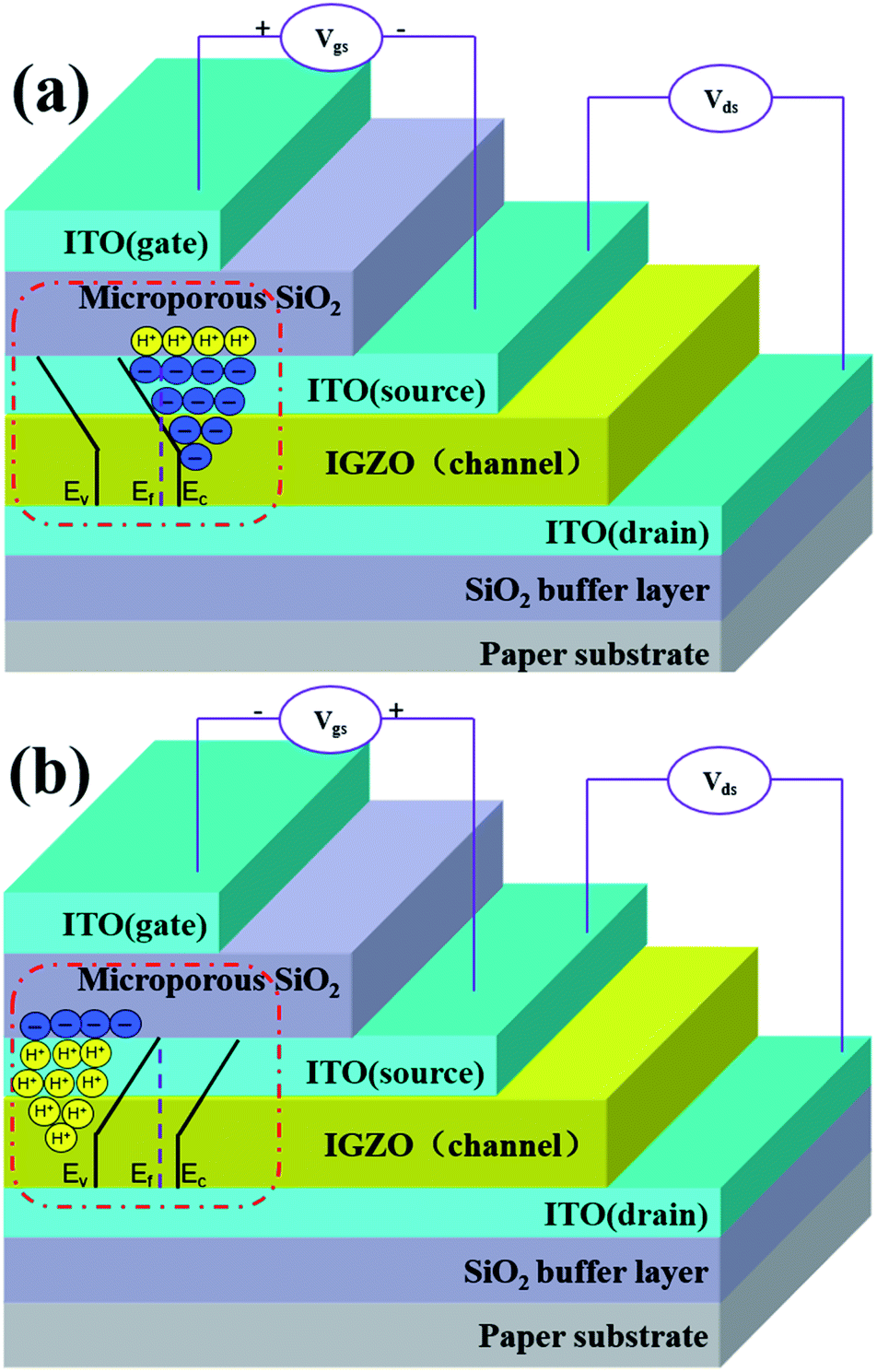 | ||
| Fig. 1 Schematic diagram of flexible EDL vertical IGZO channel TFT with a top gate. (a) Red box: band diagram for the device biased with a positive gate voltage (Vgs > 0 V). (b) Red box: band diagram for the device biased with a positive gate voltage (Vgs < 0 V). | ||
Results and discussion
To understand the operating mechanism of such vertical IGZO channel TFTs, an energy band model is proposed. Before contacting, the conduction band and the valence band of ITO source and IGZO channel are horizontally distributed, the Fermi levels (Ef) are within the conduction band and band gap respectively. After contacting, the system will achieve a uniform Ef. Finally, the energy bands in the surface of vertical IGZO channel bending downwards because of the build-in electric field induced by the free electrons inject from the source to the channel.8 When a positive Vgs is applied, high-density electrons will be induced and the surface energy bands bend downwards, as shown in the red box of Fig. 1(a), in this case, our vertical IGZO channel TFTs are turned on with a large on-state current. If a negative Vgs is applied to the gate electrode, the electrons in the ITO source and IGZO channel will be depleted, and the surface energy bands bend upwards, in this case, the device would be turned off, as shown in the red box of Fig. 1(b). The surface roughness of paper substrate can be improved by the SiO2 buffer layer, the smooth surface and interface can improve the electrical performance of paper TFTs, which has been proved in our previous work.9Fig. 2(a) shows the schematic diagram of EDL formation and low-voltage operation mechanism of the flexible EDL vertical IGZO channel TFTs with a top gate. In general, during the PECVD process, the hydrogen dissociated from SiH4 in the plasma can enter the microporous SiO2 dielectric, which can induce some mobile protons in SiO2 layer as reported in the literature.10 However, bare proton should not exist in SiO2. What is most often referred to as the “proton” is almost certainly associated with a bridging oxygen atom to form a three coordinate oxygen centre (Si–OH+–Si).11 The schematic diagram of the working mechanism for the EDL TFTs is shown in Fig. 2(a), which can be described as follows. When a negative gate voltage is applied to the gate electrode, protons will move to the gate electrode/SiO2-dielectric interface and the device is turned off. When a positive gate voltage is applied, protons move to a thin boundary layer at the SiO2-dielectric/ITO source interface, and the positive charge induces an image charge and opposite sign in the ITO source layer, which is similar to the case of the EDL formation in organic transistors gated by ionic liquids or solid state electrolytes. This large EDL gate capacitance of 3.8 μF cm−2 results in a very low operating voltage of 1.0 V. The capacitance of the microporous SiO2 was characterized by the capacitance–frequency (C–f) measurement using an Agilent 4294A precision impedance analyzer, as shown in Fig. 2(b). Remarkably, the C–f characteristics shows that the capacitance of the microporous SiO2 dielectric deposited by PECVD at room temperature reaches a maximum of 3.8 μF cm−2 at 40 Hz and down to 0.79 μF cm−2 at 104 Hz although the thickness of this microporous-SiO2 is 4.0 μm. The relationship between the microporous SiO2 capacitance and frequency is consistent with ion gel dielectrics.12 The proton mobility in this 4.0 μm microporous SiO2 limits the switching speed of TFTs, so the frequency dependence of this microporous SiO2 capacitance is strong, which requires the migration of protons to form the EDL. The huge capacitance at low frequencies was mainly profited from the response of the EDL at the microporous SiO2/ITO interface.
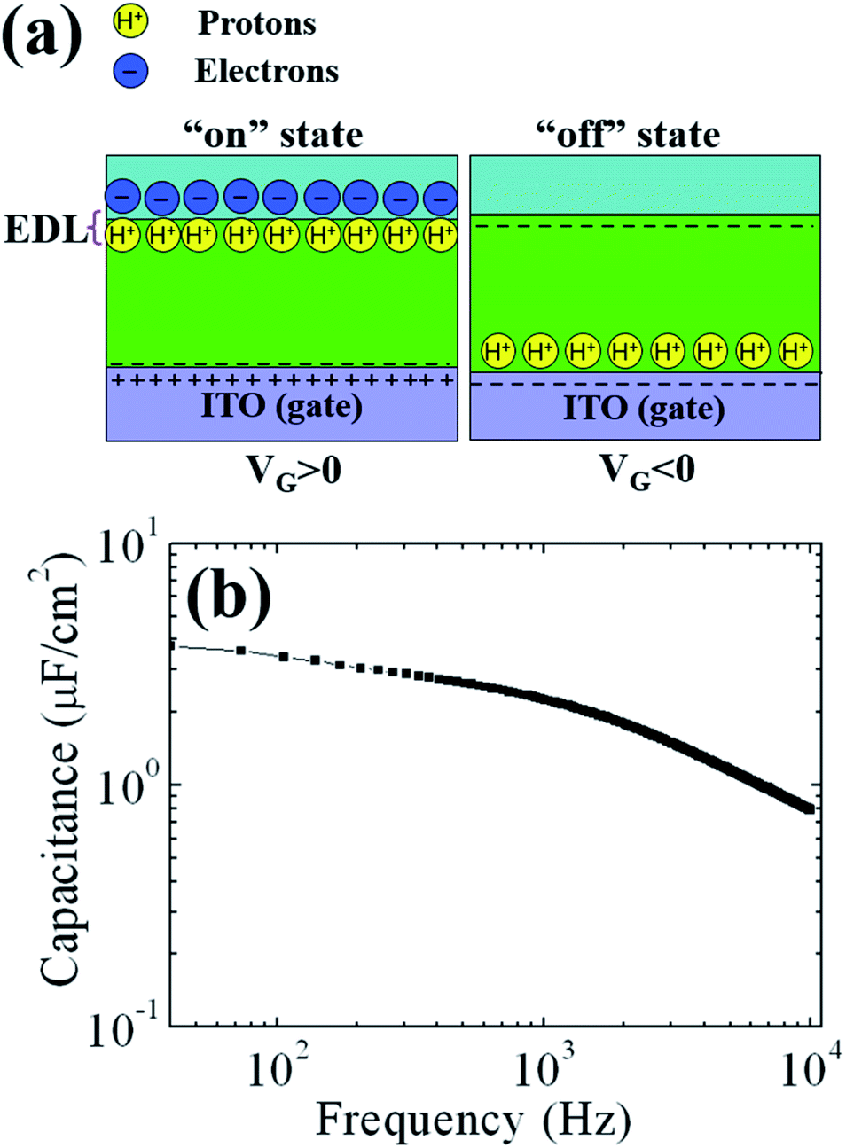 | ||
| Fig. 2 (a) Schematic diagram of EDL formed in the vertical IGZO channel TFTs gated by microporous SiO2. (b) The C–f characteristics for microporous-SiO2 dielectric. | ||
Fig. 3(a) shows the typical output characteristics (Vds–Ids) for flexible EDL vertical IGZO channel TFTs with a top gate. The Vgs was varied from 0 to 0.6 V in 0.2 V steps. The device operated in n-type field-effect transistor behaviors with a depletion mode because an obvious drain current was measured when Vgs = 0 V. A high saturation current of 0.67 mA was obtained under the bias conditions of Vds = 0.8 V and Vgs = 0.6 V. The hard saturation reveals that the Fermi level in the channel is effectively controlled by the gate and drain voltages. The Vds–Ids curves did not show any evidence of current crowding at low Vds, which indicates good ohmic contact between ITO source/drain electrodes and vertical IGZO channel. The corresponding transfer characteristics at fixed Vds = 1.0 V are shown in Fig. 3(b). The subthreshold gate voltage swing S = dVgs/d(logIds), defined as the voltage required to increase the drain current by a factor of 10. The smaller the S, the easier it is to switch the transistor to an off state. For the as-fabricated TFT, the subthreshold slope S is estimated to be 80 mV per decade. The current on/off ratio is calculated to be about 1.2 × 10⁶ with a low off current of 0.76 nA. The high output current (∼1 mA) at less than 1.0 V for this device is remarkably attractive for devices needing high drive current at low voltage, such as organic light-emitting diodes.13 Note that negligibly small hysteresis (∼50 mV) in the transfer characteristic when the gate voltage sweeping from −1.0 V to +1.0 V and back. Such small hysteresis is mainly due to the mobile protons in the microporous SiO2 dielectric. According to the equation of N = ΔVthCOX/e, where ΔVth is the threshold voltage shift between the dual sweeping of transfer curve, the COX is the capacitance per unit area, the proton density is calculated to be 1.2 × 1012 cm−2.
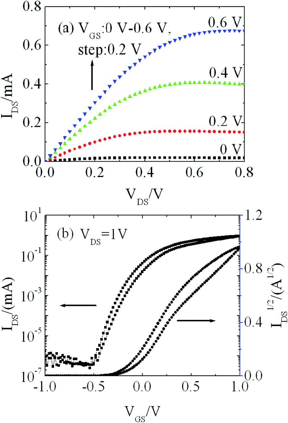 | ||
| Fig. 3 (a) Typical output characteristics and (b) transfer characteristics of flexible EDL vertical IGZO channel TFTs with a top gate. | ||
The gate leakage current (Ig) of the microporous SiO2 gate dielectric deposited by PECVD at room temperature is shown in Fig. 4. Leakage current is about 1.0 nA under the bias of 0.8 V, which is acceptable for our vertical IGZO channel TFTs operation. This small leakage current is likely due to the electrochemical silence and the small ionic current in microporous SiO2. Despite the porosity in gate dielectric, the leakage current is six orders of magnitude smaller than the channel current, which assures the field-effect performance will not be affected by the leakage.
 | ||
| Fig. 4 Gate leakage current (Ig–Vgs) curve of the measured TFT. | ||
The comparison of electrical performance of such vertical channel TFTs with other works is shown in Table 1. The electrical performance of such vertical channel paper TFTs is much better than that of other works. The operating voltage of such vertical channel paper TFT is much lower than other works with smaller SS.
Conclusions
In conclusion, huge EDL capacitance was measured in microporous SiO2-based solid-electrolyte deposited by PECVD method at room temperature. Flexible vertical IGZO channel TFTs with a top gate gated by such EDL dielectric operate in an n-type depletion mode with a low operation voltage of 1.0 V. The threshold voltage, drain current on/off ratio and subthreshold swing are estimated to be −0.1 V, 1.2 × 10⁶ and 80 mV per decade, respectively. The combination of low voltage and room-temperature processing demonstrate that flexible EDL vertical IGZO channel TFTs with a top gate are very promising for low power portable flexible electronics.Funding
This work was supported by Research Foundation of Education Bureau of Hunan Province (Grant No. 20B345, 18A009), Doctoral Science Foundation of Hunan Normal University (Grant No. 0531120), National Science Foundation of China (Grant No. 12074116, 51102091, 11574081), Natural Science Foundation of Hunan Province (Grant No. 2020RC1003, 2020JJ4424), Open Foundation of Guangxi Key Laboratory of Processing for Non-ferrous Metals and Featured Materials, Guangxi University (Grant No. 2021GXYSOF07).Author contributions
LHL and WD performed the experiments and drafted the manuscript with the help of YYT, XY, JLZ, YKW, SZZ, SYD, HTG, WCZ and DST. All authors read and approved the final manuscript.Conflicts of interest
There are no conflicts to declare.Notes and references
- B. H. Wang, A. Thukral, Z. Q. Xie, L. M. Liu, X. N. Zhang, W. Huang, X. G. Yu, C. J. Yu, T. J. Marks and A. Facchetti, Nat. Commun., 2020, 11, 2405 CrossRef CAS PubMed.
- Y. Kusaka, N. Shirakawa, S. Ogura, J. Leppaniemi, A. Sneck, A. Alastalo, H. Ushijima and N. Fukuda, ACS Appl. Mater. Interfaces, 2018, 10, 24339–24343 CrossRef CAS PubMed.
- B. H. Wang, L. Zeng, W. Huang, F. S. Melkonyan, W. C. Sheets, L. F. Chi, M. J. Bedzyk, T. J. Marks and A. Facchetti, J. Am. Chem. Soc., 2016, 138, 7067–7074 CrossRef CAS PubMed.
- C. Kulchaisit, J. P. S. Bermundo, M. N. Fujii, Y. Ishikawa and Y. Uraoka, AIP Adv., 2018, 8, 095001 CrossRef.
- J. Z. Sheng, T. H. Hong, H.-M. Lee, K. R. Kim, M. Sasase, J. Kim, H. Hosono and J.-S. Park, ACS Appl. Mater. Interfaces, 2019, 11, 40300–40309 CrossRef CAS.
- Y. Zhang, S. Yu, K. Lan, L. Li and G. Qin, AIP Adv., 2019, 9, 015111 CrossRef.
- I.-D. Kim, Y. W. Choi and H. L. Tuller, Appl. Phys. Lett., 2005, 87, 043509 CrossRef.
- W. N. Hu, Z. M. Zheng and J. Jiang, Org. Electron., 2017, 44, 1–5 CrossRef CAS.
- W. Dou, J. Jiang, J. Sun, B. Zhou and Q. Wan, IEEE Electron Device Lett., 2011, 32, 1543–1545 CAS.
- F. Yan, P. Migliorato and Y. Hong, Appl. Phys. Lett., 2005, 86, 253504 CrossRef.
- J. Godet and A. Pasquarello, Phys. Rev. Lett., 2006, 97, 155901 CrossRef PubMed.
- J. H. Cho, J. Lee, Y. Xia, B. Kim, Y. He, M. J. Renn, T. P. Lodge and C. D. Frisbie, Nat. Mater., 2008, 7, 900 CrossRef CAS PubMed.
- P. F. Carcia, R. S. McLean and M. H. Reilly, Appl. Phys. Lett., 2006, 88, 123509 CrossRef.
- X. Yin, S. Deng, G. Li, W. Zhong, R. Chen, G. Li, F. S. Y. Yeung, M. Wong and H. S. Kwok, IEEE Electron Device Lett., 2020, 41, 248–251 CAS.
- H. R. Kim, M. Furuta and S. M. Yoon, ACS Appl. Electron. Mater., 2019, 1, 2363–2370 CrossRef CAS.
- R. Verma, C. K. Suman and R. Srivastava, Thin Solid Films, 2018, 666, 156–160 CrossRef CAS.
| This journal is © The Royal Society of Chemistry 2021 |