DOI:
10.1039/D1RA01231B
(Paper)
RSC Adv., 2021,
11, 17901-17909
A comparative study of electrical and opto-electrical properties of a few-layer p-WSe2/n-WS2 heterojunction diode on SiO2 and h-BN substrates†
Received
15th February 2021
, Accepted 12th May 2021
First published on 18th May 2021
Abstract
Since the innovation of van der Waals heterostructures of 2D materials, the p–n junction diode, a building block of electronics and opto-electronics has been studied in various ways. To date most of them have been studied on SiO2 or other oxide substrates, although the oxide substrates cause significant degradation of the 2D material's intrinsic properties and device performances. Whereas using hexagonal boron nitride (h-BN) as an underlying layer to the 2D materials is known to preserve their properties. Here we have carefully analyzed the electrical and opto-electrical properties of a p-WSe2/n-WS2 van der Waals heterojunction diode on SiO2 and the h-BN substrates. Besides the usual enhancement of the field-effect mobility of WSe2 and WS2, we have achieved a significant enhancement of the diode rectification ratio and excellent photovoltaic characteristics on the h-BN substrate. We have obtained more than an order-of-magnitude enhancement of the diode rectification ratio and about two-fold increments in the overall opto-electronics behavior on the h-BN substrate compared with those on the SiO2 substrate. The values of self-powered photo responsivity and external quantum efficiency are 3 A/W and 588% respectively on the h-BN substrate at 10 mW cm−2 photo-power density and 633 nm wavelength, whereas they reduce to about one-half on the SiO2 substrate.
Introduction
Graphene has been excessively studied in the field of electronics,1,2 optoelectronics3,4 and spintronics,5–7 although the zero band-gap nature of pristine graphene hinders its application in electronic devices.8,9 On the other hand, the 2D transition metal dichalcogenide (TMD) materials with a band-gap ranging from 1 eV to 2 eV depending on their layer thickness are excellent alternatives to graphene.10 The band-gap also varies from a multilayer indirect gap to a monolayer direct gap,11,12 providing possibilities for wide application such as in photo-detectors,13,14 optical communication,15,16 and field-effect transistors.17,18 Among the TMD family, tungsten (W) and molybdenum (M) based TMDs are in great demand due to their unique and superior semiconducting and optoelectronic properties.19–21 Of the W-based TMDs, tungsten disulphide (WS2) has attracted much attention because of its high field-effect mobility, larger spin–orbit coupling,22,23 high photo sensitivity in the visible region,24 and abundance in n-type doping. Similarly tungsten diselenide (WSe2) is at the apex of interest because of its high mobility, less degradation in an ambient environment,25 high photo-absorbance coefficient in the longer wavelength region, and dominant p-type doping.26–28 Formation of a p–n heterojunction between p-WSe2 and n-WS2 produces a strong type-II band alignment and hence a high built-in potential,29,30 which is excellent for opto-electronic device applications. Among the different types of van der Waals (vdW) p–n heterojunction diodes, the lateral–vertical heterostructure has attracted considerable attention and showed better performance, whereas few studies have been done on a true vertical or in-plane lateral heterojunction structure.31–33
Since the beginning, almost all the research work on the vdW p–n heterojunction diode has been done on SiO2 or other oxide substrates.34 Experimental findings suggest that the qualities of 2D materials including graphene, TMDs, and many others on the oxide substrate were affected by various factors such as scattering from charged surface states, surface impurities, and surface roughness.35–37 In particular, the charge impurities trapped at the interface between the 2D material and SiO2 were found to change the intrinsic properties of the materials.38 Furthermore, it has been proved that the major source of hysteresis, which hinders the device performance and stability, also arises from the trapped charges. Without addressing these problems, we cannot obtain a fine tune of the material's intrinsic characteristics and realize the actual device performance and stability, which was overlooked by most of the research done before on the p–n junction diodes.29–33 Among the 2D materials, hexagonal boron nitride (h-BN) is known to be a good supporting substrate to address those problems, owing to the inert nature, high band-gap energy (5.5 eV), and high dielectric constant (∼4).35 Furthermore, atomically planner and smooth surface of h-BN reduces the rippling in the 2D materials, lowers the trapped charge density, and also reduces the hysteresis, thereby enhancing the field-effect mobility of the 2D materials.36,38–40
Herein we report a comparative study of electronic and opto-electronic behaviors of p-WSe2/n-WS2 heterojunction diodes fabricated on both SiO2 and h-BN substrates. Our main motivation towards this work is to systematically study the substrate's influence on the device performances. We observed more than an order-of-magnitude increment of the diode rectification ratio on the h-BN substrate than on the SiO2 substrate. Moreover, the calculated photovoltaic parameters indicate significantly improved photo-electric behaviors in h-BN supported device as compared to SiO2 supported device.
Experimental
Device fabrication
A mechanical exfoliation technique with a transparent polydimethylsiloxane (PDMS) stamp was used to transfer suitable TMD and h-BN flakes from high quality natural bulk crystals. The WS2 crystal was purchased from 2D semiconductors, and WSe2 and h-BN crystals from HQ graphene. Flakes of each material were mechanically exfoliated by using an adhesive tape. Then, they were picked up by a PDMS stamp on a glass slide for the transfer process. The uniformity and the thickness of the exfoliated flakes were roughly identified with an optical microscope before the transfer, and confirmed later by the atomic force microscopy (AFM). Placing the PDMS stamp on a target substrate and peeling it off transfers the flakes to the substrate. Successive transfers of few layers (FL) WSe2 and FL WS2 on the SiO2/Si substrate makes a WS2/WSe2/SiO2 lateral–vertical p–n vdW heterojunction diode, now onward named as device1. To prepare the h-BN substrate, a large uniform multilayer h-BN flake was first transferred onto another SiO2/Si substrate and then it was annealed at 300 °C for 2 hours in high vacuum (>10−6 torr) to remove the residues present. Finally, FL WSe2 and FL WS2 flakes were successively transferred over the h-BN so that it makes a WS2/WSe2/h-BN/SiO2 lateral–vertical p–n heterojunction diode, now onward named as device2. The transfer of each flake was precisely controlled with a micro-aligner stage monitored by a CCD camera. After the transfer of each TMD flake it was passed through a 1 hour hot acetone bath to remove the PDMS and tape residues. For the electrodes, a high work-function metal Pd for the p-type WSe2 and a low work-function metal Al for the n-type WS2 were deposited followed by a 60 nm-thick Au cap layer under high vacuum condition. Optical microscope images of the device1 and device2 are shown in Fig. 1(a) and (b), respectively, and their schematics in (c) and (d), respectively. With the two contacts placed on each of the TMD flakes, electrical characteristics of each TMD or the heterojunction could be measured.
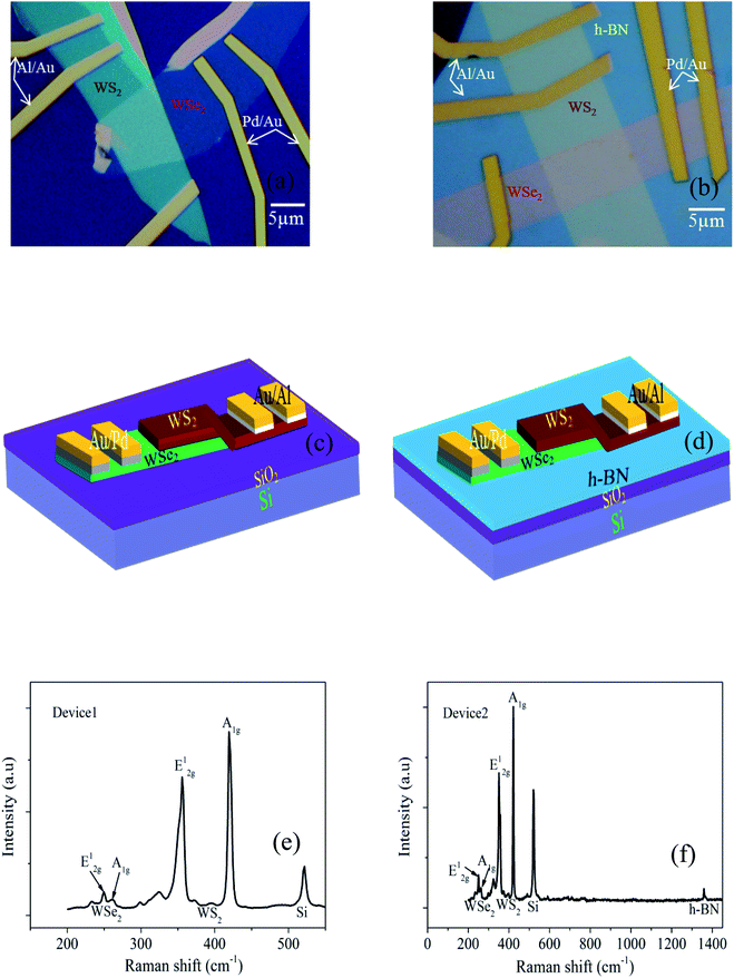 |
| | Fig. 1 (a) and (b) An optical microscopic image of the p-WSe2/n-WS2 heterojunction diode of device1 and device2 respectively. (c) and (d) Schematic device geometry of device1 and device2, respectively. (e) and (f) Raman spectra of device1 and device2 at the junction with laser excitation wavelength of 514 nm. | |
Measurements
Raman spectroscopy for the devices were done with Renishaw RE04 model with the wavelength of 514 nm under 1 mW power and laser spot size of about 1 μm. Height profiles of the devices were measured with an AFM (NanoFocus) along with the surface topography. For electrical transport measurements we have used Keithley 2400 source-meter and Keithley 6485 pico-ammeter. Photoresponse was measured using a wave generated by LGK 7654-13 He–Ne laser (633 nm) under vacuum condition.
Results and discussion
Raman spectroscopy and AFM
The Raman spectroscopy data for both devices at the heterojunction region are shown in Fig. 1(e) and (f). The two typical Raman active modes of WSe2, E12g (250 cm−1) and A1g (260 cm−1), were observed.41 Similarly we obtained two Raman peaks at 350 and 420 cm−1, representing E12g and A1g modes of WS2.42 Raman peaks from the substrates, Si (520 cm−1) for the device1 and both Si (520 cm−1) and h-BN (1350 cm−1) for the device2 are also shown. Detailed spectrums of each individual flake of WS2 and WSe2 are shown in Fig. S1.† Furthermore, we conducted an AFM (NanoFocus) measurement to verify the flake thicknesses. Fig. S2(a) and (b)† show the combined height profile of WSe2 (∼5.8 nm) and WS2 (∼8.0 nm) of device1 and WSe2 (∼5.6 nm) and WS2 (∼8.8 nm) of device2 with inset AFM topographic images. The thickness of h-BN is 30 nm as shown in Fig. S2(c).†
Electrical characteristics of p-WSe2/n-WS2 heterojunction
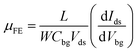
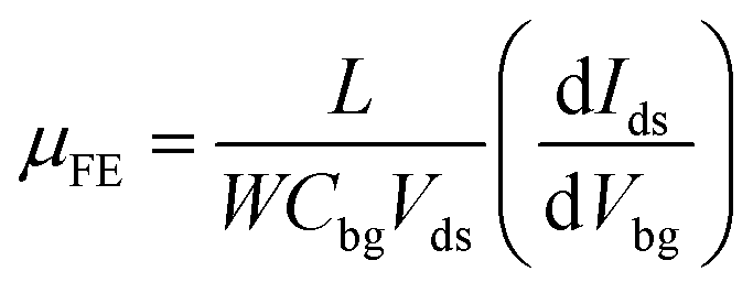
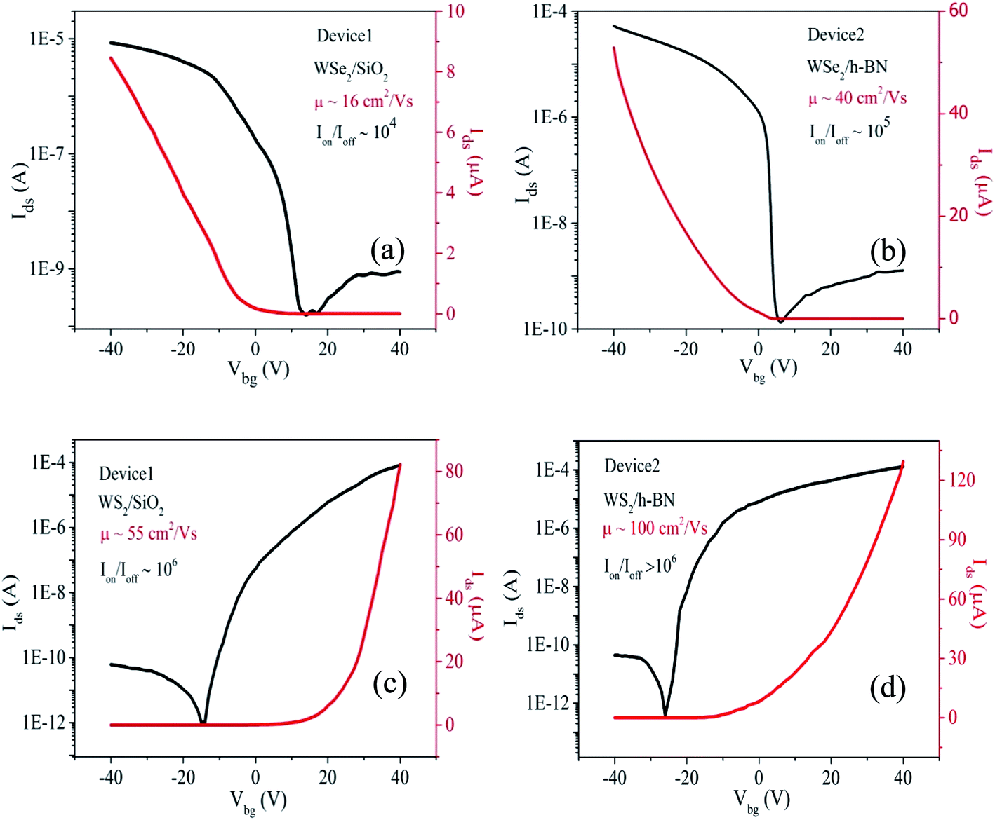
The transfer characteristics curve, source-drain current (Ids) as a function of back-gate voltage (Vbg), of WSe2 on the two devices at a source-drain voltage (Vds) of 1 V are plotted in Fig. 2(a) and (b). The increment of Ids at negative Vbg confirms the p-type nature of WSe2 on both substrates. Fig. 2(c) and (d) show the transfer characteristics curve of WS2 on both devices, where the n-type nature of WS2 is confirmed from the increment of Ids at positive Vbg. The field-effect mobility (μFE) and the ION/IOFF ratio of each TMD were calculated in both devices to analyze the electrical performance. We have used the relation below to extract μFE of the TMDs in both devices.| |
 | (1) |
where L and W denote the length and width of the TMDs channel,  is the slope of the linear part of transfer characteristics curve, and Cbg is the gate-capacitance of the substrates. The gate-capacitance can be calculated by
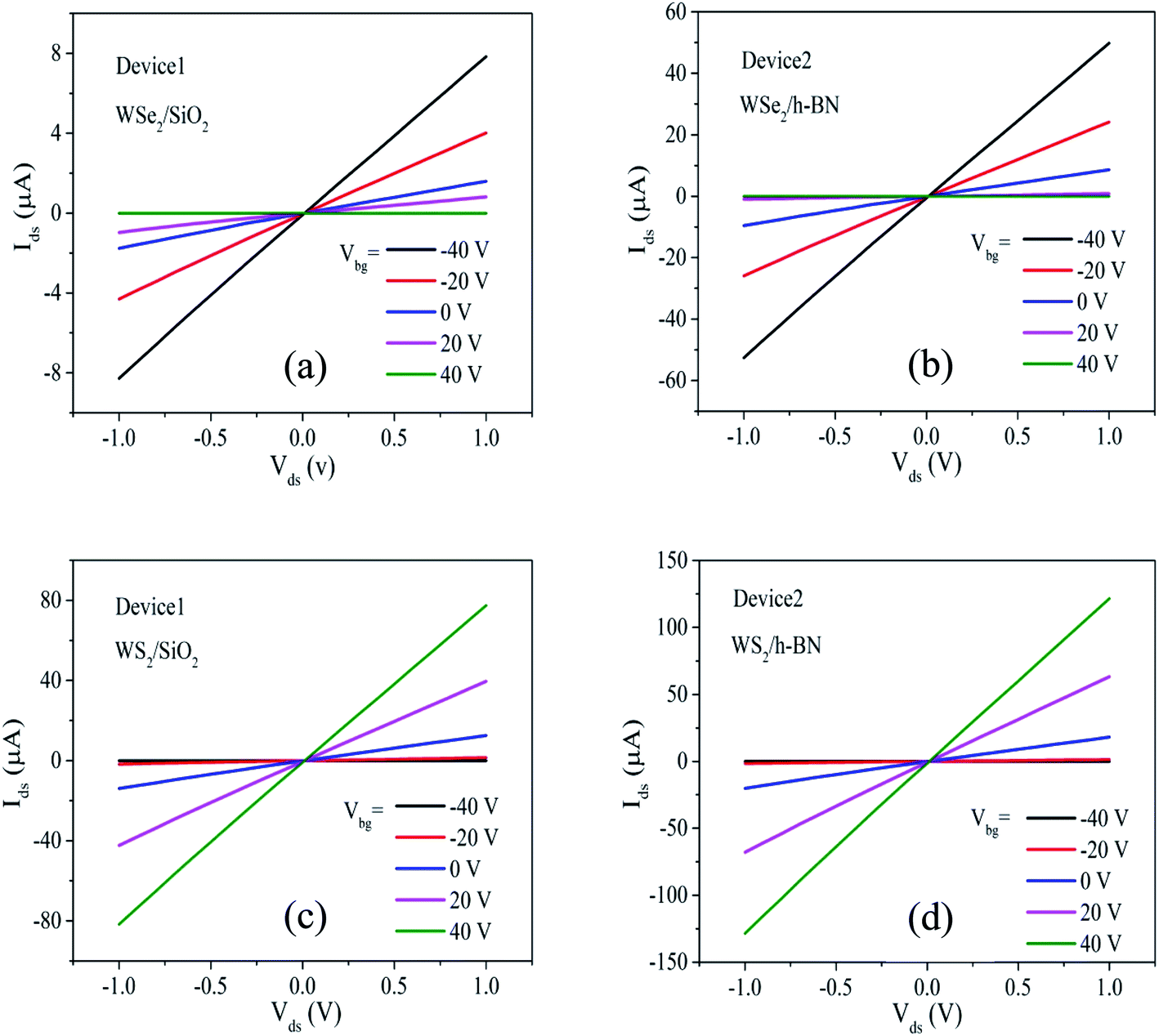
  43,44 where εr is the relative permittivity of SiO2 (3.9) and d is the thickness. The value of Cbg we have obtained is 287 μF m−2. For the h-BN/SiO2 structure, the gate-capacitance should include the contribution of both dielectrics being that of two capacitors in series but the h-BN could be neglected since its thickness is much smaller than the SiO2. The mobility of WS2 and WSe2 we obtained in device2 was 100 and 40 cm2 V−1 s−1 respectively, which is about 2 times higher than those measured in device1. The ION/IOFF ratio in device 2 increases about an order-of-magnitude reaching 105 for WSe2 and a three-fold increment for WS2 as compared to those in device1. The main reason behind the significant enhancement in the filed-effect mobility and ION/IOff ratio of the TMDs in device2 is the use of the h-BN substrate, as explained by the articles published.35,43,45 Furthermore, the charge injection from suitable metal contacts into the TMDs also helps to enhance the device characteristics as suggested by articles.46,47 Pd is one of the best contact metal for an efficient hole injection into WSe2 because of its high work-function and better alignment to the valance band of WSe2,27,48 whereas low work-function metal Al is one of the suitable candidates for n-type materials and hence reduces the Schottky barrier height (SBH), thereby making ohmic contacts. Fig. 3(a) and (b) illustrate the current–voltage (Ids–Vds) curves of p-WSe2 on device1 and device2, respectively, whereas (c) and (d) show those of n-WS2 on device1 and device2, respectively, at different back-gate voltages. The contacts between the metal and the TMD in both devices show linear behavior, insuring low contact resistance.
 |
| | Fig. 2 Transfer characteristics curve (Ids–Vbg) of each FL flake on different substrates at Vds = 1 V. (a) and (b) FL-WSe2 showing p-type characteristic on SiO2 and h-BN substrates respectively. (c) and (d) FL-WS2 showing n-type characteristic on SiO2 and h-BN substrate respectively. | |
 |
| | Fig. 3 Linear Ids–Vds characteristics curve of TMDs at different Vbg on different substrates. (a) and (b) FL-WSe2 on SiO2 and h-BN substrates respectively. (c) and (d) FL-WS2 on SiO2 and h-BN substrates respectively. | |
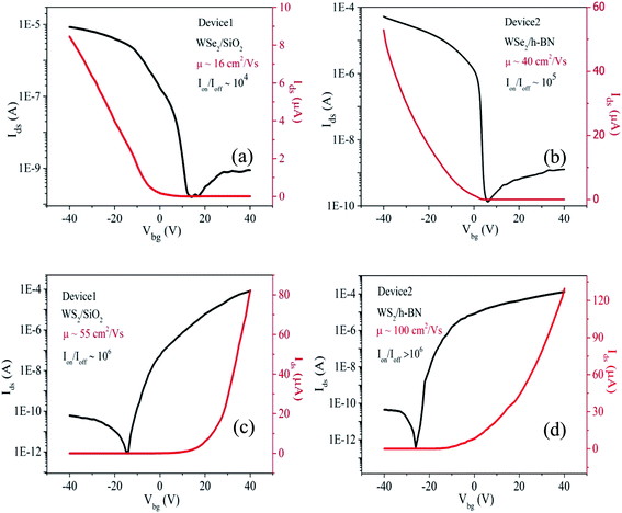
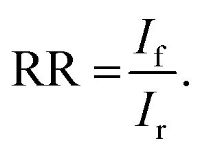
Now we discuss the rectification behavior of the p-WSe2/n-WS2 heterojunction diode. The Ids–Vds characteristics curves of the p–n heterojunction with Vbg = −40 V is shown in Fig. 4. Diode rectification ratio (RR) was defined by the ratio of the forward current (If) to the reverse current (Ir),  We have observed the diode RR as high as 105 in device1, which is in the range of previously reported values on the SiO2 substrate,49,50 whereas an order-of-magnitude enhancement is achieved in device2 (h-BN substrate) with RR > 106. There are several different factors influencing the diode RR. The diode RR was believed to be limited by a high SBH of the metal/TMD interface. This limiting effect was confirmed after the achievement of a high diode RR with an ohmic metal/TMD interface and a much reduced SBH.51 As another factor, the sharpness of the interface between the TMDs at the junction is still under debate.32,52 Generally most of the diode characteristics have been studied in a lateral–vertical vdW heterojunction structure, where lateral channels are also present in addition to the heterojunction.32,53 The diode RR in a true vertical heterojunction without the lateral channel was found significantly lower than the lateral–vertical heterojunction.32 It suggests that the planer TMD channel along with the vertical TMD junction plays a crucial role. Most of all, the h-BN substrate plays an important role to enhance the diode RR in our experiment as compared with the SiO2 substrate. If we compare the semi-log plot of the Ids–Vds curves at Vbg = −40 V in Fig. 4(b), the reverse current in device2 (h-BN substrate) is about an order-of-magnitude smaller whereas the forward current is slightly lower than those of device1 (SiO2 substrate). This suggests that the TMD/SiO2 interface introduces more trap states, which cause the large reverse current as well as the unintentional forward current.54 The reduction of hysteresis behavior in device2 as compared to device1 further confirms less trapped states at the TMD/h-BN interface, as shown in Fig. S3.† Furthermore, the h-BN substrate significantly reduces the surface defects and provides a flat and inert base for the device. Therefore, our p–n heterojunction diode in device2 showed much improved Ids–Vds characteristics as compared to device1. We also show the Vbg dependent Ids–Vds characteristics curves in Fig. S4.†
 |
| | Fig. 4 Diode (Ids–Vds) characteristics curves of p-WSe2/n-WS2 heterojunction at Vbg = −40 V. (a) Linear scale (b) semi-log scale. | |
Opto-electrical characteristics of p-WSe2/n-WS2 heterojunction
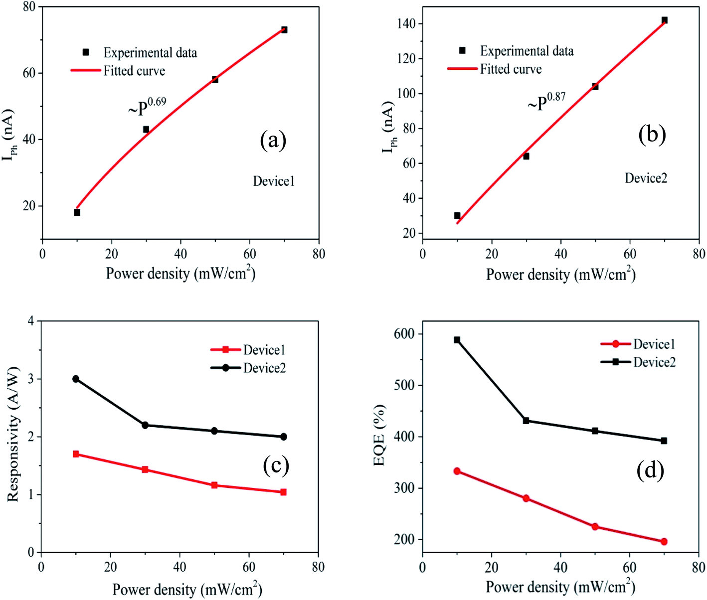
Along with the excellent electric properties, the p-WSe2/n-WS2 lateral–vertical heterojunction also exhibits superior photovoltaic properties. The output (Ids–Vds) curves under different photo-power densities (P) of 10, 30, 50, and 70 mW cm−2 at the wavelength (λ) of 633 nm are shown in Fig. 5(a) and (b) for device1 and device2. In both devices we observed a significant change in the Ids–Vds characteristics with photo powers. Huo et al.30 also observed a large photo response in a p-WSe2/n-WS2 heterojunction that is comparable to our results in device1. The large photovoltaic behavior occurs mainly due to the type-II band alignment and the high built-in potential at the heterointerface, which can effectively separate the photo-excited electron–hole pairs. These electrons and holes are accumulated towards the n-WS2 and p-WSe2, respectively, and lead to the formation of an open-circuit voltage (VOC), the P-dependence of which is shown in Fig. 5(c). These accumulated electrons and holes in WS2 and WSe2 recombine rapidly through an external circuit leading to the generation of a short-circuit current (ISC) at zero Vds, as shown in Fig. 5(d). We observed larger values of VOC and ISC in device2 than in device1, which is attributed to the excellent photo absorption and efficient photo-induced electron–hole pair generation in device2 as compared to that of device1. Accordingly, a significantly improved time dependent photocurrent is observed in device2 compared to that of device1 as shown in Fig. 5(e). The photocurrent can be instantly generated and declined with switching the light on and off. Basically, the h-BN substrate makes an inert and flat surface, which reduces the scattering effects and the trap states.49,50 The trap states on the SiO2 substrate capture the electron–hole pairs generated by the photo power thereby reduce the photocurrent.55 We checked the trap states in both devices by fitting the photocurrent (Iph = Iillumination − Idark) plotted as a function of P at Vds = 0 V with the power–law equation Iph = aPα, where a is a scaling constant and α an exponent,30,56 as shown in Fig. 6(a) and (b) for device1 and device2 respectively. The value of α closer to 1 indicates a higher efficiency of photo-excited electron–hole pair generation and also indicates fewer trap states at the junction (α = 1 for ideal case). In our case α in device2 is about 0.87, which is higher than 0.69 in device1 indicating lower trap states in device2 with the h-BN substrate.
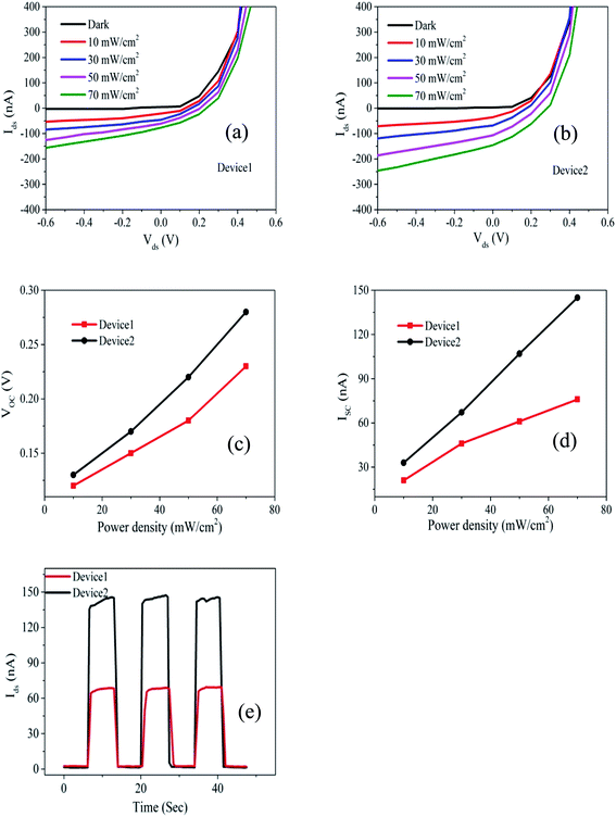 |
| | Fig. 5 Photo responses of p-WSe2/n-WS2 heterojunction on different substrates under the illumination of light wavelength of 633 nm (at 0 Vbg). (a) and (b) Ids–Vds characteristics curves under different power density on SiO2 and h-BN substrates respectively. (c) VOC (d) ISC plotted as a function of power density. (e) The dynamic response of both devices with P = 70 mW cm−2 at 0 Vds and 0 Vbg. | |
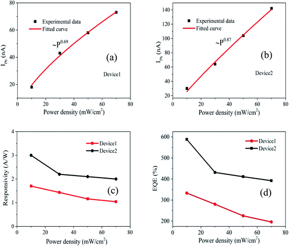 |
| | Fig. 6 (a) and (b) Self-driven photocurrent (IPh) vs. incident photo-power density on device1 and device2 respectively, where red curves show the power-law fitting. (c) and (d) Responsivity and EQE as a function of power density, respectively. | |
We also calculated the photo-responsivity (R) and external quantum efficiency (EQE). R is defined by where S is the junction area of the device. We show R as a function of P with 0 Vds and 0 Vbg in Fig. 6(c). The observed increase of R as P decreases is in consistence with the articles published before.30,57,58 R is about 3.0 A W−1 and 1.6 A W−1 with power density of 10 mW cm−2 for device2 and device1, respectively. The EQE is defined as the number of photo-generated carriers per incident photons per second and expressed as
  where h is the Planck's constant, c the speed of light, and e the elementary charge. The value of EQE depends on the photo absorption and the accumulation of photo-generated carriers. Fig. 6(d) illustrates the values of EQE as a function of P at 0 Vds and 0 Vbg. EQE is about 588% at 10 mW cm−2 for device2, which is about 2 times higher than that for the device1. These values we obtained in device2 are far better than the values reported before with the identical conditions in TMD heterostructures.28–30,58,59 The higher values of R and EQE in our device2 is mainly attributed to the use of h-BN substrate, which enhances the photo absorption and the photocurrent due to the lower trap states,59,60 as well as the excellent photo response of WSe2 (ref. 61–63) and WS2 (ref. 24) as compared to other TMDs. In addition, a fast photo-carrier separation and the resulting short transit time due to the large built-in potential may contribute to a significant gain and the large EQE.58,64,65
Conclusion
We have investigated the electric and opto-electric properties of p-WSe2/n-WS2 vdW heterojunction diode on SiO2 and h-BN substrates. The device on the h-BN substrate showed much enhanced diode characteristics. We have achieved more than an order-of-magnitude enhancement in the diode RR (>106) and better device stability with h-BN substrate over the SiO2 substrate. Moreover, overall two-fold higher values were obtained in the photovoltaic characteristics on the h-BN substrate. Particularly, the values of self-powered photo responsivity and EQE we have obtained are 3 A W−1 and 588% on the h-BN substrate at P = 10 mW cm−2 and λ = 633 nm. These values are superior to the values reported before at the identical conditions. The overall excellent results in device2 are mainly attributed to the use of inert, flat, and defect-free h-BN substrate, which reduces the carriers to be trapped in defect states. Moreover the heterostructure formed by highly photosensitive WS2 and WSe2 also plays a crucial role for the excellent photovoltaic outcome. To conclude, diode characteristics either electrical or opto-electrical can be significantly improved with the use of h-BN as a substrate and also with an appropriate selection of TMDs for the heterostructure.
Conflicts of interest
There are no conflicts to declare.
Acknowledgements
This work was supported by the National Research Foundation of Korea (NRF) grant funded by the Korea government (MSIT) (No. NRF-2020R1F1A1071556).
References
- A. H. Castro Neto, et al., The electronic properties of graphene, Rev. Mod. Phys., 2009, 81(1), 109–162 CrossRef CAS.
- T. Ando, The electronic properties of graphene and carbon nanotubes, NPG Asia Mater., 2009, 1(1), 17–21 CrossRef.
- F. Bonaccorso, et al., Graphene photonics and optoelectronics, Nat. Photonics, 2010, 4(9), 611 CrossRef CAS.
- F. H. Koppens, D. E. Chang and F. J. Garcia de Abajo, Graphene plasmonics: a platform for strong light–matter interactions, Nano Lett., 2011, 11(8), 3370–3377 CrossRef CAS PubMed.
- N. Tombros, et al., Electronic spin transport and spin precession in single graphene layers at room temperature, Nature, 2007, 448(7153), 571–574 CrossRef CAS PubMed.
- P. Zomer, et al., Long-distance spin transport in high-mobility graphene on hexagonal boron nitride, Phys. Rev. B, 2012, 86(16), 161416 CrossRef.
- P. R. Sharma, et al., Magnetoresistance effect in a vertical spin valve fabricated with a dry-transferred CVD graphene and a resist-free process, Mater. Res. Express, 2020, 7, 085603 CrossRef CAS.
- A. A. Green and M. C. Hersam, Emerging methods for producing monodisperse graphene dispersions, J. Phys. Chem. Lett., 2010, 1(2), 544–549 CrossRef CAS PubMed.
- D. C. Elias, et al., Control of graphene's properties by reversible hydrogenation: evidence for graphane, Science, 2009, 323(5914), 610–613 CrossRef CAS PubMed.
- K. Novoselov, Nobel lecture: Graphene: Materials in the flatland, Rev. Mod. Phys., 2011, 83(3), 837 CrossRef CAS.
- M. Kang, et al., Universal mechanism of band-gap engineering in transition-metal dichalcogenides, Nano Lett., 2017, 17(3), 1610–1615 CrossRef CAS PubMed.
- Q. Wang, K. Kalantar-Zadeh, A. Kis, J. N. Coleman and M. S. Strano, Nat. Nanotechnol., 2012, 7, 699–712 CrossRef CAS PubMed.
- H. Tan, et al., Ultrathin 2D photodetectors utilizing chemical vapor deposition grown WS2 with graphene electrodes, ACS Nano, 2016, 10(8), 7866–7873 CrossRef CAS PubMed.
- F. Koppens, et al., Photodetectors based on graphene, other two-dimensional materials and hybrid systems, Nat. Nanotechnol., 2014, 9(10), 780–793 CrossRef CAS PubMed.
- Z. Sun, A. Martinez and F. Wang, Optical modulators with 2D layered materials, Nat. Photonics, 2016, 10(4), 227–238 CrossRef CAS.
- J. A. Tatum and J. K. Guenter, Consumer electronics with optical communication interface, US Pat. 7,706,692, 2010 Search PubMed.
- B. Radisavljevic, M. B. Whitwick and A. Kis, Integrated circuits and logic operations based on single-layer MoS2, ACS Nano, 2011, 5(12), 9934–9938 CrossRef CAS PubMed.
- H. Fang, et al., Degenerate n-doping of few-layer transition metal dichalcogenides by potassium, Nano Lett., 2013, 13(5), 1991–1995 CrossRef CAS PubMed.
- F. Dybała, et al., Pressure coefficients for direct optical transitions in MoS2, MoSe2, WS2, and WSe2 crystals and semiconductor to metal transitions, Sci. Rep., 2016, 6, 26663 CrossRef PubMed.
- J. Kopaczek, et al., Direct optical transitions at K-and H-point of Brillouin zone in bulk MoS2, MoSe2, WS2, and WSe2, J. Appl. Phys., 2016, 119(23), 235705 CrossRef.
- G. Rubio-Bollinger, et al., Enhanced visibility of MoS2, MoSe2, WSe2 and black-phosphorus: making optical identification of 2D semiconductors easier, Electronics, 2015, 4(4), 847–856 CrossRef CAS.
- H. Yuan, et al., Zeeman-type spin splitting controlled by an electric field, Nat. Phys., 2013, 9(9), 563–569 Search PubMed.
- D. Xiao, et al., Coupled spin and valley physics in monolayers of MoS2 and other group-VI dichalcogenides, Phys. Rev. Lett., 2012, 108(19), 196802 CrossRef PubMed.
- N. Huo, et al., Photoresponsive and gas sensing field-effect transistors based on multilayer WS2 nanoflakes, Sci. Rep., 2014, 4, 5209 CrossRef CAS PubMed.
- A. Eftekhari, Tungsten dichalcogenides (WS2, WSe2, and WTe2): materials chemistry and applications, J. Mater. Chem. A, 2017, 5(35), 18299–18325 RSC.
- H. Li, et al., Mechanical exfoliation and characterization of single-and
few-layer nanosheets of WSe2, TaS2, and TaSe2, Small, 2013, 9(11), 1974–1981 CrossRef CAS PubMed.
- H. Fang, et al., High-performance single layered WSe2 p-FETs with chemically doped contacts, Nano Lett., 2012, 12(7), 3788–3792 CrossRef CAS PubMed.
- N. Flöry, et al., A WSe2/MoSe2 heterostructure photovoltaic device, Appl. Phys. Lett., 2015, 107(12), 123106 CrossRef.
- M. M. Furchi, et al., Photovoltaic effect in an electrically tunable van der Waals heterojunction, Nano Lett., 2014, 14(8), 4785–4791 CrossRef CAS PubMed.
- N. Huo, et al., Tunable Polarity Behavior and Self-Driven Photoswitching in p-WSe2/n-WS2 Heterojunctions, Small, 2015, 11(40), 5430–5438 CrossRef CAS PubMed.
- Y. Gong, et al., Vertical and in-plane heterostructures from WS2/MoS2 monolayers, Nat. Mater., 2014, 13(12), 1135–1142 CrossRef CAS PubMed.
- R. Zhou, V. Ostwal and J. Appenzeller, Vertical versus lateral two-dimensional heterostructures: on the topic of atomically abrupt p/n-junctions, Nano Lett., 2017, 17(8), 4787–4792 CrossRef CAS PubMed.
- X. Duan, et al., Lateral epitaxial growth of two-dimensional layered semiconductor heterojunctions, Nat. Nanotechnol., 2014, 9(12), 1024–1030 CrossRef CAS PubMed.
- L. Liao, et al., Single-layer graphene on Al2O3/Si substrate: better contrast and higher performance of graphene transistors, Nanotechnology, 2009, 21(1), 015705 CrossRef PubMed.
- C. R. Dean, et al., Boron nitride substrates for high-quality graphene electronics, Nat. Nanotechnol., 2010, 5(10), 722–726 CrossRef CAS PubMed.
- M. Ishigami, et al., Atomic structure of graphene on SiO2, Nano Lett., 2007, 7(6), 1643–1648 CrossRef CAS PubMed.
- R. Decker, et al., Local electronic properties of graphene on a BN substrate via scanning tunneling microscopy, Nano Lett., 2011, 11(6), 2291–2295 CrossRef CAS PubMed.
- C. Lee, et al., Comparison of trapped charges and hysteresis behavior in hBN encapsulated single MoS2 flake based field effect transistors on SiO2 and hBN substrates, Nanotechnology, 2018, 29(33), 335202 CrossRef PubMed.
- E. Wu, et al., Dynamically controllable polarity modulation of MoTe2 field-effect transistors through ultraviolet light and electrostatic activation, Sci. Adv., 2019, 5(5), eaav3430 CrossRef CAS PubMed.
- M. W. Iqbal, et al., High-mobility and air-stable single-layer WS2 field-effect transistors sandwiched between chemical vapor deposition-grown hexagonal BN films, Sci. Rep., 2015, 5, 10699 CrossRef CAS PubMed.
- W. Zhao, et al., Lattice dynamics in mono-and few-layer sheets of WS2 and WSe2, Nanoscale, 2013, 5(20), 9677–9683 RSC.
- A. Berkdemir, et al., Identification of individual and few layers of WS2 using Raman Spectroscopy, Sci. Rep., 2013, 3(1), 1755 CrossRef.
- X. Zhang, et al., Defect-controlled nucleation and orientation of WSe2 on hBN: a route to single-crystal epitaxial monolayers, ACS Nano, 2019, 13(3), 3341–3352 CrossRef CAS PubMed.
- G.-H. Lee, et al., Flexible and transparent MoS2 field-effect transistors on hexagonal boron nitride-graphene heterostructures, ACS Nano, 2013, 7(9), 7931–7936 CrossRef CAS PubMed.
- Y. Uchiyama, et al., Indirect bandgap of hBN-encapsulated monolayer MoS2. arXiv preprint arXiv:1903.06427, 2019 Search PubMed.
- C. Kim, et al., Fermi level pinning at electrical metal contacts of monolayer molybdenum dichalcogenides, ACS Nano, 2017, 11(2), 1588–1596 CrossRef CAS PubMed.
- A. Rai, et al., Progress in contact, doping and mobility engineering of MoS2: an atomically thin 2D semiconductor, Crystals, 2018, 8(8), 316 CrossRef.
- A. Allain and A. Kis, Electron and Hole Mobilities in Single-Layer WSe2, ACS Nano, 2014, 8(7), 7180–7185 CrossRef CAS PubMed.
- Y. Deng, et al., Black phosphorus–monolayer MoS2 van der Waals heterojunction p–n diode, ACS Nano, 2014, 8(8), 8292–8299 CrossRef CAS PubMed.
- R. Cheng, et al., Electroluminescence and photocurrent generation from atomically sharp WSe2/MoS2 heterojunction p–n diodes, Nano Lett., 2014, 14(10), 5590–5597 CrossRef CAS PubMed.
- A. M. Afzal, et al., Tunneling-based rectification and photoresponsivity in black phosphorus/hexagonal boron nitride/rhenium diselenide van der Waals heterojunction diode, Nanoscale, 2020, 12(5), 3455–3468 RSC.
- C.-H. Lee, et al., Atomically thin p–n junctions with van der Waals heterointerfaces, Nat. Nanotechnol., 2014, 9(9), 676 CrossRef CAS PubMed.
- H.-M. Li, et al., Ultimate thin vertical p–n junction composed of two-dimensional layered molybdenum disulfide, Nat. Commun., 2015, 6(1), 1–9 CAS.
- P. J. Jeon, et al., Dipole-containing encapsulation on WSe2/MoS2 nanoflake pn diode with glass substrate toward an ideal performance. arXiv preprint arXiv:1412.7593, 2014.
- M. Hafeez, et al., Large-area bilayer ReS2 film/multilayer ReS2 flakes synthesized by chemical vapor deposition for high performance photodetectors, Adv. Funct. Mater., 2016, 26(25), 4551–4560 CrossRef CAS.
- M. Wasala, et al., Effect of underlying boron nitride thickness on photocurrent response in molybdenum disulfide-boron nitride heterostructures, J. Mater. Res., 2016, 31(7), 893 CrossRef CAS.
- G. Konstantatos, et al., Hybrid graphene–quantum dot phototransistors with ultrahigh gain, Nat. Nanotechnol., 2012, 7(6), 363–368 CrossRef CAS PubMed.
- H. Luo, et al., High-Responsivity Photovoltaic Photodetectors Based on MoTe2/MoSe2 van der Waals Heterojunctions, Crystals, 2019, 9(6), 315 CrossRef CAS.
- X. Wei, et al., Photodetectors based on junctions of two-dimensional transition metal dichalcogenides, Chin. Phys. B, 2017, 26(3), 038504 CrossRef.
- G. Nazir, et al., Comparison of electrical and photoelectrical properties of ReS2 field-effect transistors on different dielectric substrates, ACS Appl. Mater. Interfaces, 2018, 10(38), 32501–32509 CrossRef CAS PubMed.
- N. R. Pradhan, et al., High photoresponsivity and short photoresponse times in few-layered WSe2 transistors, ACS Appl. Mater. Interfaces, 2015, 7(22), 12080–12088 CrossRef CAS PubMed.
- J. Lu, et al., Atomic healing of defects in transition metal dichalcogenides, Nano Lett., 2015, 15(5), 3524–3532 CrossRef CAS PubMed.
- W. Zhang, et al., Role of metal contacts in high-performance phototransistors based on WSe2 monolayers, ACS Nano, 2014, 8(8), 8653–8661 CrossRef CAS PubMed.
- N. Oliva, et al., Van der Waals MoS2/VO2 heterostructure junction with tunable rectifier behavior and efficient photoresponse, Sci. Rep., 2017, 7(1), 14250 CrossRef PubMed.
- M. Hussain, et al., NIR self-powered photodetection and gate tunable rectification behavior in 2D GeSe/MoSe2 heterojunction diode, Sci. Rep., 2021, 11(1), 3688 CrossRef CAS PubMed.
Footnote |
| † Electronic supplementary information (ESI) available. See DOI: 10.1039/d1ra01231b |
|
| This journal is © The Royal Society of Chemistry 2021 |
Click here to see how this site uses Cookies. View our privacy policy here. 
 Open Access Article
 This Open Access Article is licensed under a Creative Commons Attribution-Non Commercial 3.0 Unported Licence
 b and
Hwayong Noh
b and
Hwayong Noh
 is the slope of the linear part of transfer characteristics curve, and Cbg is the gate-capacitance of the substrates. The gate-capacitance can be calculated by
 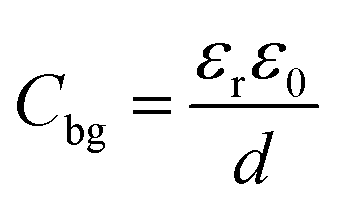 43,44 where εr is the relative permittivity of SiO2 (3.9) and d is the thickness. The value of Cbg we have obtained is 287 μF m−2. For the h-BN/SiO2 structure, the gate-capacitance should include the contribution of both dielectrics being that of two capacitors in series but the h-BN could be neglected since its thickness is much smaller than the SiO2. The mobility of WS2 and WSe2 we obtained in device2 was 100 and 40 cm2 V−1 s−1 respectively, which is about 2 times higher than those measured in device1. The ION/IOFF ratio in device 2 increases about an order-of-magnitude reaching 105 for WSe2 and a three-fold increment for WS2 as compared to those in device1. The main reason behind the significant enhancement in the filed-effect mobility and ION/IOff ratio of the TMDs in device2 is the use of the h-BN substrate, as explained by the articles published.35,43,45 Furthermore, the charge injection from suitable metal contacts into the TMDs also helps to enhance the device characteristics as suggested by articles.46,47 Pd is one of the best contact metal for an efficient hole injection into WSe2 because of its high work-function and better alignment to the valance band of WSe2,27,48 whereas low work-function metal Al is one of the suitable candidates for n-type materials and hence reduces the Schottky barrier height (SBH), thereby making ohmic contacts. Fig. 3(a) and (b) illustrate the current–voltage (Ids–Vds) curves of p-WSe2 on device1 and device2, respectively, whereas (c) and (d) show those of n-WS2 on device1 and device2, respectively, at different back-gate voltages. The contacts between the metal and the TMD in both devices show linear behavior, insuring low contact resistance.
 We have observed the diode RR as high as 105 in device1, which is in the range of previously reported values on the SiO2 substrate,49,50 whereas an order-of-magnitude enhancement is achieved in device2 (h-BN substrate) with RR > 106. There are several different factors influencing the diode RR. The diode RR was believed to be limited by a high SBH of the metal/TMD interface. This limiting effect was confirmed after the achievement of a high diode RR with an ohmic metal/TMD interface and a much reduced SBH.51 As another factor, the sharpness of the interface between the TMDs at the junction is still under debate.32,52 Generally most of the diode characteristics have been studied in a lateral–vertical vdW heterojunction structure, where lateral channels are also present in addition to the heterojunction.32,53 The diode RR in a true vertical heterojunction without the lateral channel was found significantly lower than the lateral–vertical heterojunction.32 It suggests that the planer TMD channel along with the vertical TMD junction plays a crucial role. Most of all, the h-BN substrate plays an important role to enhance the diode RR in our experiment as compared with the SiO2 substrate. If we compare the semi-log plot of the Ids–Vds curves at Vbg = −40 V in Fig. 4(b), the reverse current in device2 (h-BN substrate) is about an order-of-magnitude smaller whereas the forward current is slightly lower than those of device1 (SiO2 substrate). This suggests that the TMD/SiO2 interface introduces more trap states, which cause the large reverse current as well as the unintentional forward current.54 The reduction of hysteresis behavior in device2 as compared to device1 further confirms less trapped states at the TMD/h-BN interface, as shown in Fig. S3.† Furthermore, the h-BN substrate significantly reduces the surface defects and provides a flat and inert base for the device. Therefore, our p–n heterojunction diode in device2 showed much improved Ids–Vds characteristics as compared to device1. We also show the Vbg dependent Ids–Vds characteristics curves in Fig. S4.†
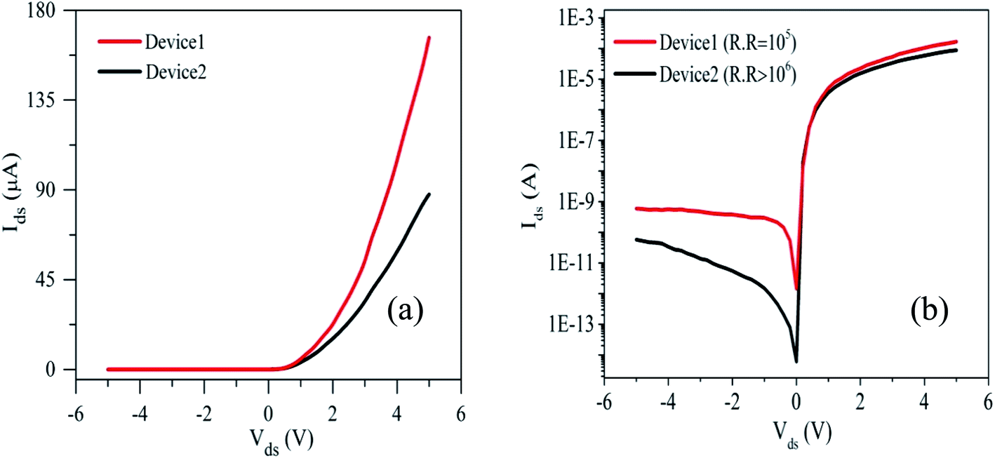

 where S is the junction area of the device. We show R as a function of P with 0 Vds and 0 Vbg in Fig. 6(c). The observed increase of R as P decreases is in consistence with the articles published before.30,57,58 R is about 3.0 A W−1 and 1.6 A W−1 with power density of 10 mW cm−2 for device2 and device1, respectively. The EQE is defined as the number of photo-generated carriers per incident photons per second and expressed as
  where h is the Planck's constant, c the speed of light, and e the elementary charge. The value of EQE depends on the photo absorption and the accumulation of photo-generated carriers. Fig. 6(d) illustrates the values of EQE as a function of P at 0 Vds and 0 Vbg. EQE is about 588% at 10 mW cm−2 for device2, which is about 2 times higher than that for the device1. These values we obtained in device2 are far better than the values reported before with the identical conditions in TMD heterostructures.28–30,58,59 The higher values of R and EQE in our device2 is mainly attributed to the use of h-BN substrate, which enhances the photo absorption and the photocurrent due to the lower trap states,59,60 as well as the excellent photo response of WSe2 (ref. 61–63) and WS2 (ref. 24) as compared to other TMDs. In addition, a fast photo-carrier separation and the resulting short transit time due to the large built-in potential may contribute to a significant gain and the large EQE.58,64,65