
 Open Access Article
 This Open Access Article is licensed under a Creative Commons Attribution-Non Commercial 3.0 Unported Licence
Tunable electron property induced by B-doping in g-C3N4†
Bo Yang *a,
Hongxia Bub and
Xiaobiao Liuc
*a,
Hongxia Bub and
Xiaobiao Liuc
aSchool of Science, Shandong Jianzhu University, Jinan 250101, China. E-mail: yangbo19@sdjzu.edu.cn
bCollege of Physics and Electronic Engineering, Qilu Normal University, Jinan 250200, China
cSchool of Science, Henan Agricultural University, Zhengzhou 450002, China
First published on 27th April 2021
Abstract
Graphitic carbon nitrides are a research hotspot of two-dimensional (2D) materials, which attract more and more attention from researchers. Topological properties are a focus in graphitic carbon nitrides materials. Using first-principles calculations, we modified the g-C3N4 (formed by tri-s-triazine) by B atoms, proposing a novel two-dimensional monolayer, g-C6N7B, which showed excellent stability verified by positive phono modes, molecular dynamic simulations and mechanical criteria. The valence band and conduction band touch at the Γ point. Interestingly, g-C6N7B is topologically nontrivial, because the valance and conduction band can be gapped by the spin–orbit coupling (SOC) effect associated with robust gapless edge states. Additionally, molecular dynamic simulations indicate that g-C6N7B will still maintain good geometry structure when the temperature is as high as 1500 K. The flexibility of g-C6N7B is confirmed by its elastic constants and Young's moduli. This work opens an avenue for graphitic carbon nitride materials with topological properties.
Introduction
Since the successful synthesis of the graphene monolayer,1 it has shown many excellent properties. However, another type of two-dimensional monolayer, graphitic carbon nitrides, which have a similar framework to graphene, have attracted a great deal of researchers' attention in recent years. In fact, graphitic carbon nitrides were studied by Franklin as early as 1922.2 There are two prevailing units, s-triazine (C3N3) and tri-s-triazine (C6N7), forming the framework of graphitic carbon nitrides materials.3–7 These frameworks were synthesized by chemical synthetic approaches under relatively mild conditions.6,8–14 Among the graphitic carbon nitrides, the framework with the formula of C3N4 (named g-C3N4), has a major advantage, that is, high thermal and chemical stability.15 Initially, researchers found that g-C3N4 can be applied in many fields, such as fuel cells, hydrogen production, and photocatalysis.16–19 It is disappointing to note that the gap of g-C3N4 is 2.88 eV,20 which is too wide induced the utilization of visible light in the photocatalytic reaction is too low.21,22 Doping or replanting element is an effective strategy to improve the performance of g-C3N4.23–32 Based on the above studies, g-C3N4 has been found many other exotic properties in a similar way, such as spin polarize33–35 and topological properties.36Topological insulators (TIs) are a novel quantum state, which with a bulk gap under spin–orbit interaction and protected by gapless edge states or surface states, leading to the quantum spin Hall (QSH) effect.37 Graphene is theoretical predicted to be a two-dimensional (2D) topological insulator,38 which was considered to be the first material capable of achieving the QSH effect. Then, because of special lattice structure and stable edge states of 2D materials, 2D TIs become a new research hotspot in condensed matter physics. As we all know, g-C3N4 has great potential in the catalytic application. However, the topological study of 2D graphitic carbon nitrides monolayer is quite rarely. A. Zhu et al. proposed a new 2D topological insulator material, g-C6N6 in which the s-triazines are separated via C–C bonds.39 Therefore, we used one B atom to replace the central N atom in the g-C3N4, which is composed of tri-s-triazine unit with a chemical ratio is C6N8, formed g-C6N7B, which is a topological 2D material.
In this work, we study the electronic, topological, and mechanical properties of g-C6N7B on the basis of first-principles calculations. Firstly, the dynamical and mechanical stability of g-C6N7B was verified from the phonon spectrum, molecular dynamics simulations, and elastic constants, respectively. Our calculated results indicated that the conduction band and valence band of g-C6N7B touch with each other at Γ point. The conduction and valence band opened a small gap with spin–orbit coupling (SOC) interaction. Additionally, we also calculated the edge states of g-C6N7B, which showed that the band structure of edge states is gapless. More interestingly, molecular dynamics simulations calculations showed that the g-C6N7B monolayer can maintain its original configuration at temperatures up to 1500 K. And, the in-plane Young's moduli are only two-five of that of graphene, revealed the ultra-softness of g-C6N7B monolayer. More interesting, there has two absorption peaks in ultraviolet region.
Method and computational details
We performed first-principles calculations based on density functional theory (DFT), implemented by the Vienna ab initio simulation package (VASP).40 The generalized gradient approximation (GGA) in the form of the Perdew–Burke–Ernzerhof (PBE) was adopted for the exchange-correlation functional.41 The electron–ion interaction was described by projector-augmented-wave (PAW) potentials.42 The energy cutoff employed for plane-wave expansion of electron wavefunction was set to 400 eV. The Brillouin zone (BZ) integration was sampled on a grid of 6 × 6 × 1 k-points according to the Monkhorst–Pack method for structural optimization. Two-dimensional periodic boundary conditions were employed in the x–y plane, while a vacuum space up to 20 Å was applied along the z-direction to exclude the interaction between neighboring images. Structural optimizations were carried out using a conjugate gradient (CG) method until the remaining force on each atom was less than 0.01 eV Å−1. The phonon spectra were calculated by using the Phonopy code43,44 interfaced with VASP. In the whole calculation process, the correction of dispersion term is not considered. The reason is that it does not affect the properties of the system, showed in Fig. S1.†Results and discussion
We doped one B atom in a C6N7 unit replaced the center N atom, which named g-C6N7B, the geometry structure as shown in Fig. 1(a). The optimized lattice constants are a = b = 7.12 Å, which slightly deviating from that of the non-doped g-C3N4 monolayer, 7.14 Å.34 And, the optimized structure of g-C3N4B with slight deformation compared with the g-C3N4 framework. The optimized g-C6N7B structure has the C–N bond lengths of 1.34 Å (within a triazine ring) and 1.43 Å (between adjacent triazine rings), respectively. The bond lengths within the triazine ring are very similar to that of g-C3N4 (1.33 Å). However, the C–N bond lengths between the adjacent triazine rings are shorter than that of g-C3N4 (1.46 Å). Additionally, the C–B bond lengths are 1.49 Å.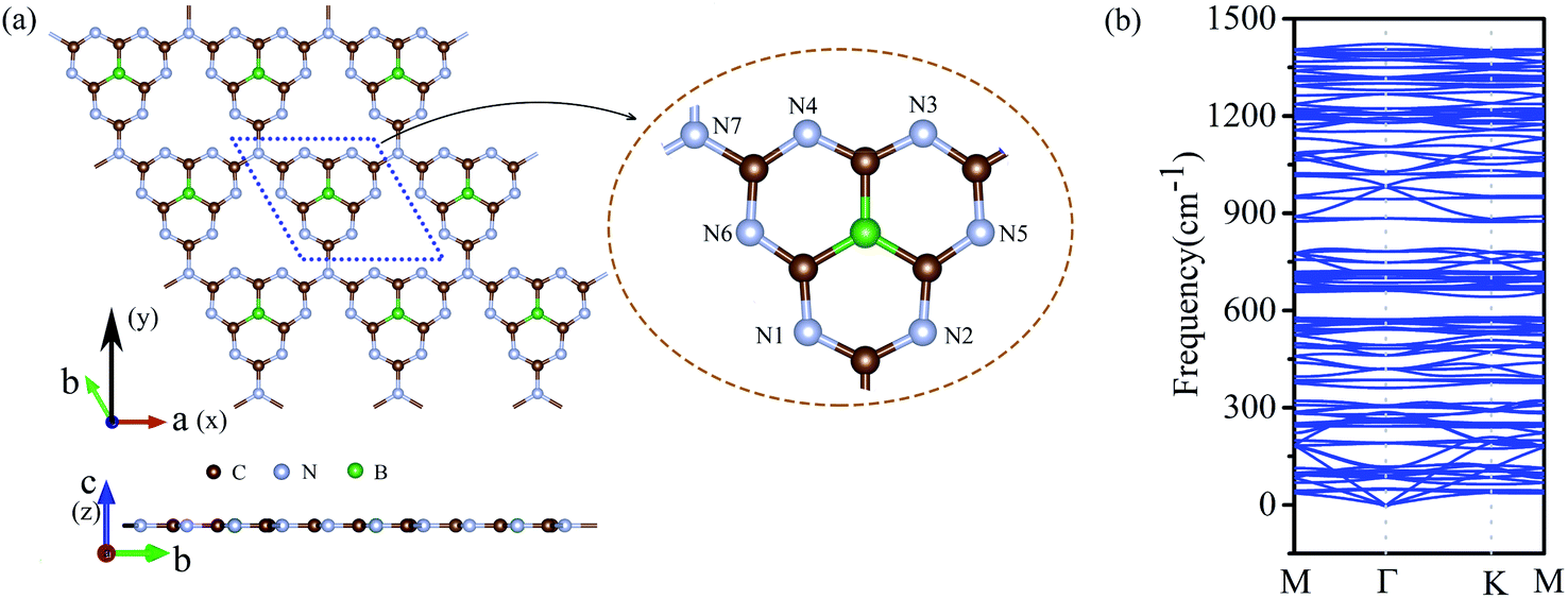 | ||
| Fig. 1 (a) The top (upper) and the side (lower) view of the geometric structure of g-C6N7B monolayer. (b) The phonon spectrum of g-C6N7B along the highly symmetric directions in the BZ. | ||
Next, we discussed the stability of g-C6N7B by different methods. First, we confirmed the dynamic stability of g-C6N7B from the phonon spectrum obtained by using a supercell approach within the PHONOPY code. From Fig. 1(b), it can be clearly seen that the phonon spectrum is free from imaginary frequency modes. Remarkably, the highest frequency of g-C6N7B reaches up to 1422 cm−1, which much higher than those of MoS2 monolayer (473 cm−1),45 silicene (580 cm−1)46 and even higher than that of h-BN (1301 cm−1),47 suggesting strong bonds in the g-C6N7B.
To verify the stability of g-C6N7B at room temperature (300 K), we performed the molecular dynamics simulations with the Nose–Hoover thermostat at 300 K and a time step of 1.0 fs. After running 5000 steps, the geometry of g-C6N7B was well preserved without any structure collapse and the total energy of the system was converged in this time scale, as shown Fig. 2 (a) and (b). Due to previous reports, we found that the non-doped g-C3N4 and B/S/P doped g-C3N4 is synthesized at high temperature25,26,48 and g-C6N7B has the same geometry with g-C3N4. We performed the molecular dynamic simulation at 800 K, 1000 K, 1500 K, the total energy of the system was converged after running 5000 fs, showed in Fig. 2(c)–(e). We also checked the geometries structure of g-C6N7B, found that the geometries structure maintained very well compared with the original the configuration of g-C6N7B at temperatures up to 1500 K, as shown in Fig. 2(f). The result showed that g-C6N7B is a high temperature resistant material. The above results indicated that the g-C6N7B exhibits high thermal stability.
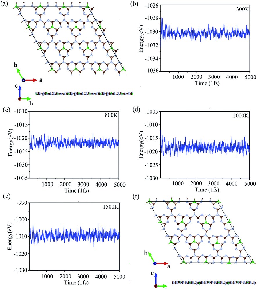 | ||
| Fig. 2 (a) and (f) The geometry structure of g-C6N7B with respect to the simulation time at 300 K and 1500 K. (b)–(e) The total energy fluctuations with respect to the simulation time at 300 K, 800 K, 1000 K, 1500 K. | ||
To investigate the electronic property of g-C6N7B, we calculated its electronic band structure by using the first-principle theory without spin–orbit coupling (SOC). From Fig. 3(a), it is very clear to see that the conduction and valence bands meet each other at Γ point featured a gapless semi-conduction, which is different from the linear dispersion at K point of valence and conduction band in the band structure of graphene. In addition, the characteristic can also be verified the total density of states (TDOS) of g-C6N7B, showed in Fig. S2.† And, due to the flat conduction band, there has a significant peak near the Fermi level, showed in Fig. S2.† To show the features clearly, we plotted the electronic states near the meeting point in a 2D wave vector mesh, as shown in Fig. 3(c), which indicated the conduction and valence bands touched at Γ point. Then, by considering SOC, our DFT calculated results showed a bandgap of 5 meV opened at the Fermi level, as shown in Fig. 3(b). More detail information with the difference between the band structure with and without SOC shown in Fig S3.† The small gap is due to the weak SOC effect of the light C, N, and B elements. However, this value is much higher than the magnitude of graphene (∼10−3 meV).49 Furthermore, we used the maximally localized Wannier functions (MLWFs) method to fit the band structure within energy range [Ef −0.3, Ef +0.4] eV. It can be seen from Fig. 3(b) that the SOC gap of DFT calculations are good to agree with that by employing Wannier interpolation.
 | ||
| Fig. 3 (a) and (b) Electronic band structure of g-C6N7B without SOC and with SOC respectively. (c) The 3D band structure of conduction band and valence band. The Fermi level was set to zero. (4) The local electronic density (LDOS) calculated from edge Green's function of the semi-infinite g-C6N7B lattice. | ||
The occurrence of the energy gap due to the SOC effect reminds us of the topological nontriviality of g-C6N7B. To further demonstrate the topological nontriviality, we constructed the edge Green's function of the semi-infinite g-C6N7B lattice from MLWFs by using the Wannier90 package.50 The local density of states (LDOS) of the edge calculated from the MLWFs is plotted in Fig. 3(d). From the figure, we can see that the gapless edge state appears in the gap between the valence band and conduction band. The existence of an edge state confirms the topological nontriviality of g-C6N7B monolayer.
To analyzed the origin of electronic states near the Fermi level at Γ point, we plotted the orbital-resolved band structure projected onto different atomic orbitals, as shown in Fig. 4(b)–(k). The px orbital of N1/N5, py orbital of N3/N4, and px + py orbitals of N2/N6/B mainly to contribute the bands near the Fermi level at Γ point. However, the contribution of C atoms and joint N atoms can be neglected. The orbital-resolved band structure of other atoms was showed in Fig. S4.† The Dirac cone electronic states near Fermi level of graphene come from the pz orbital of each C atom. We also calculated the electron density profile of the Kohn-Sham wave functions at the Γ point near the Fermi level, as shown in Fig. 4(1). It is very clearly to see that the electronic states near the Fermi level are almost contributed by p orbital of N atoms and B atoms, which are in good agreement with the orbital-resolved band structure.
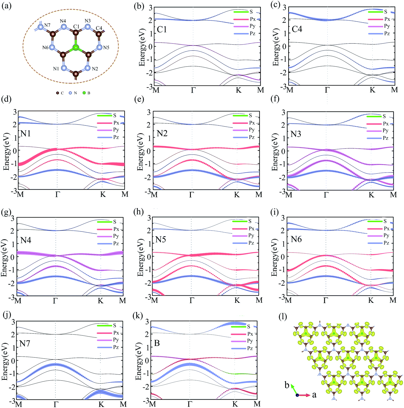 | ||
| Fig. 4 (a) The geometry structure of g-C6N7B. (b)–(k) The orbital-resolved band structure of the g-C6N7B on different atoms, labelled in (a). (l) The electron density isosurfaces of the electron Kohn-Sham wave functions at Γ point near Fermi level. | ||
Mechanical property
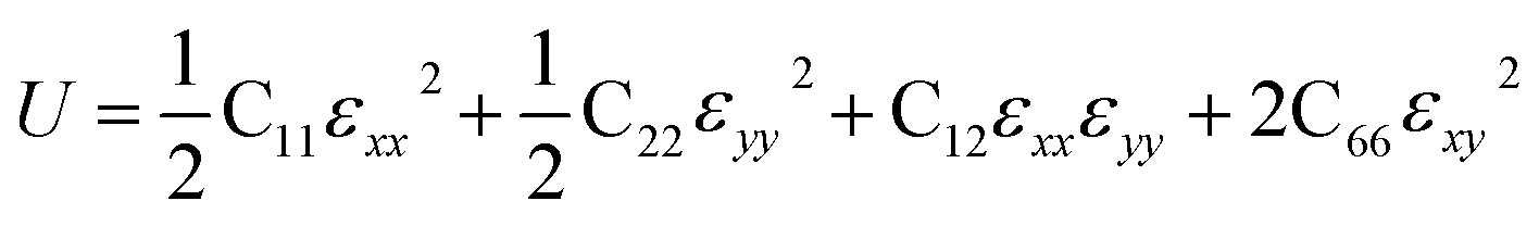
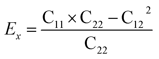
Then, we verified the mechanical stability of g-C6N7B by using the standard Voigt notation51,52 and studied its mechanical properties. The elastic energy per unit area for a 2D sheet can be expressed as:where εxx and εyy represent the uniaxial in-plane stains along x- and y-direction and εxy is the shear strain. The parameters C11, C22, C12 and C66 represent the components of the elastic modulus tensor, corresponding to the second partial derivation of strain energy with respect to strain. The elastic constants can be obtained by fitting the energy curves associated with uniaxial and equi-biaxial strain, which are C11 = 164.53 GPa nm, C22 = 169.65 GPa nm, C12 = 74.73 GPa nm, C66 = 40.44 GPa nm, respectively. The elastic constants satisfy the criteria of the mechanical stability of 2D sheet: C11 × C22 – C122 > 0, C66 > 0, indicating that the g-C6N7B monolayer is mechanically stable. To study the mechanical properties of g-C6N7B, we calculated Young's modulus. The direction-dependent in-plane Young's moduli (Ex and Ey) along the x- and y-direction derived from the elastic constants using the formulas:
 and
and 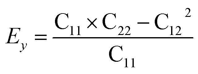 are 131.61 N m−1 and 131.71 N m−1, respectively, which is only two-five of that of graphene (335N/m),53,54 suggested that the g-C6N7B is a promising flexible material compared with graphene.
Optical property
Finally, we calculated the light absorption spectrum of g-C6N7B. From the Fig. 5, it showed that the light absorption spectral curves of g-C6N7B in x and y directions are the same with each other, indicating that the absorption capacity of g-C6N7B for different wavelengths of light shows isotropic. There are two absorption peaks in the optical absorption spectrum at 85 nm and 327 nm, which belong to the ultraviolet region. However, the peak of the absorption coefficient of graphene (x direction) at 283 nm,55 which also located in the ultraviolet region.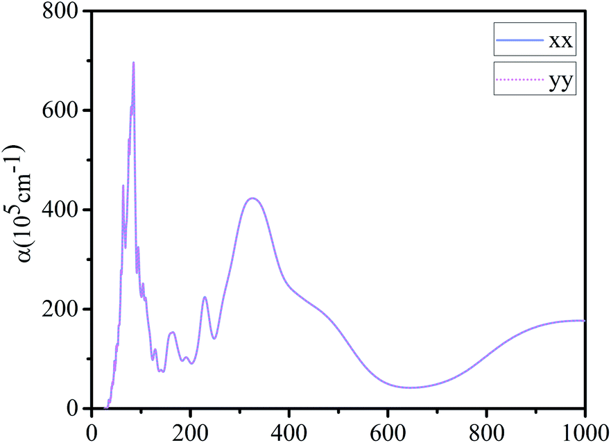 | ||
| Fig. 5 Absorption coefficient of g-C6N7B along x and y direction. | ||
Conclusion
In this paper, we replaced the central N atom in g-C3N4 with the B atom to form a new 2D monolayer, named g-C6N7B. The introduction of the B atom leads to novel electronic properties of g-C6N7B. Our calculated results showed that the conduction band and valence band touch at Γ point with gapless. However, SOC opened small band gaps between the conduction band and valence band. In addition, the topological nontrivial property of g-C6N7B was further confirmed by the appearance of gapless edge states in the g-C6N7B nanoribbon. The stability and plausibility of g-C6N7B were verified by positive phonon modes, molecular dynamical simulations, and mechanical criteria. We also calculated the molecular dynamical simulations at high temperatures, found that g-C6N7B represents excellent stability even at 1500 K. Additionally, g-C6N7B is a promising flexible material. There are two absorption peaks in the optical absorption spectrum at 85 nm and 327 nm, which belong to the ultraviolet region. These results not only enrich the graphitic carbon nitrides materials with topological property, but also establish fascinating properties of fundamental significance and practical interest.Conflicts of interest
There are no conflicts to declare.Acknowledgements
This work is supported by the Doctor Foundation of Shandong Jianzhu University (No. X20017Z), National Natural Science Foundation of China (No. 22005087).References
- K. S. Novoselov, K. A. Geim, V. S. Morozov, D. Jing, Y. Zhang, S. V. Dubonos, I. V. Grigorieva and A. A. Firsov, Science, 2004, 336, 666 CrossRef PubMed.
- E. C. Franklin, J. Am. Chem. Soc., 1922, 44, 486–509 CrossRef CAS.
- V. N. Khabashesku, J. L. Zimmerman and J. L. Margrave, Chem. Mater., 2000, 12, 3264–3270 CrossRef CAS.
- A. Thomas, A. Fischer, F. Goettmann, M. Antonietti, J. O. Müller, R. Schlögl and J. M. Carlsson, J. Mater. Chem., 2008, 18, 4893–4908 RSC.
- E. Kroke, M. Schwarz, E. Horath-Bordon, P. Kroll, B. Noll and A. D. Norman, New J. Chem., 2002, 26, 508–512 RSC.
- B. Jürgens, E. Irran, J. Senker, P. Kroll, H. Müller and W. Schnick, J. Am. Chem. Soc., 2003, 125, 10288–10300 CrossRef PubMed.
- J. Sehnert, K. Baerwinkel and J. Senker, J. Phys. Chem. B, 2007, 111, 10671–10680 CrossRef CAS.
- T. Komatsu and T. Nakamura, J. Mater. Chem., 2001, 11, 474–478 RSC.
- E. G. Gillan, Chem. Mater., 2000, 12, 3906–3912 CrossRef CAS.
- B. V. Lotsch and W. Schnick, Chem. Mater., 2005, 17, 3976–3982 CrossRef CAS.
- D. R. Miller, D. C. Swenson and E. Gillan, J. Am. Chem. Soc., 2004, 126, 5372–5373 CrossRef CAS PubMed.
- Y. C. Zhao, D. L. Yu, H. W. Zhao, Y. J. Tian and O. Yanagisawa, J. Mater. Sci., 1995, 40, 2635 Search PubMed.
- B. V. Lotsch and W. Schnick, Chem. Mater., 2006, 18, 1891–1900 CrossRef CAS.
- D. R. Miller, J. R. Hols and E. G. Gillan, Inorg. Chem., 2007, 46, 2767–2774 CrossRef CAS.
- X. Wang, K. Maeda, A. Thomas, K. Takanabe, G. Xin, J. M. Carlsson, K. Domen and M. Antonietti, Nat. Mater., 2008, 8, 76–80 CrossRef PubMed.
- X. Wang, S. Blechert and M. Antoniett, ACS Catal., 2012, 2, 1596–1606 CrossRef CAS.
- L. Ge, F. Zuo, J. Liu, Q. Ma, C. Wang, D. Sun, L. Bartels and P. Feng, J. Phys. Chem. C, 2012, 116, 13708–13714 CrossRef CAS.
- F. Wu, Y. Liu, G. Yu, D. Shen, Y. Wang and E. Kan, J. Phys. Chem. C, 2012, 115, 7355 Search PubMed.
- Y. Wang, X. Wang and M. Antonietti, Angew. Chem., 2012, 51, 68–89 CrossRef CAS.
- Y. Xu and S. P. Gao, Int. J. Hydrogen Energy, 2012, 37, 11072–11080 CrossRef CAS.
- Y. W. Zhang, J. H. Liu, G. Wu and W. Chen, Nanoscale, 2012, 4, 5300–5303 RSC.
- J. H. Liu, Y. W. Zhang, L. H. Liu, G. Wu and W. Chen, Chem. Commun., 2012, 48, 8826–8828 RSC.
- X. G. Ma, Y. H. Lv, J. Xu, Y. F. Liu, R. Q. Zhang and Y. F. Zhui, J. Phys. Chem. C, 2012, 116, 23485–23493 CrossRef CAS.
- J. S. Zhang, J. H. Sun, K. Maeda, K. Domen, P. Liu, M. Antonietti, X. Z. Fu and X. C. Wang, Energy Environ. Sci., 2011, 675–678 RSC.
- G. Liu, P. Niu, C. Sun, S. C. Smith, Z. Chen, G. Q. Lu and H. M. Cheng, J. Am. Chem. Soc., 2010, 132, 11642–11648 CrossRef CAS PubMed.
- Y. Zhang, T. Mori, J. Ye and M. Anntonietti, J. Am. Chem. Soc., 2010, 132, 6294–6295 CrossRef CAS PubMed.
- B. Yue, Q. Li, H. Iwai, T. Kako and J. Ye, Sci. Technol. Adv. Mater., 2011, 12, 034401 CrossRef PubMed.
- K. Wang, Q. Li, B. Liu, B. Cheng, W. Ho and J. Yu, Appl. Catal., B, 2015, 176, 44–52 Search PubMed.
- B. Chai, J. Yan, C. Wang, Z. Ren and Y. Zhu, Appl. Surf. Sci., 2017, 391, 376–383 CrossRef CAS.
- C. Lu, R. Chen, X. Wu, M. Fan, Y. Liu, Z. Le, S. Jiang and S. Song, Appl. Surf. Sci., 2016, 360, 1016–1022 CrossRef CAS.
- T. Tong, B. Zhu, C. Jiang, B. Cheng and J. Yu, Appl. Surf. Sci., 2018, 433, 1175–1183 CrossRef CAS.
- P. W. Chen, K. Li, Y. X. Yu and W. D. Zhang, Appl. Surf. Sci., 2017, 392, 608–615 CrossRef CAS.
- A. Du, S. Sanvito and S. C. Smith, Phys. Rev. Lett., 2012, 108, 197207 CrossRef PubMed.
- X. Zhang, M. Zhao, A. Wang, X. Zhang and A. Du, J. Mater. Chem. C, 2013, 1, 6265–6270 RSC.
- B. Yang, H. Zhou, X. Zhang and M. Zhao, J. Mater. Chem. C, 2015, 3, 10886–10891 RSC.
- A. Wang, X. Zhang and M. Zhao, Nanoscale, 2014, 6, 11157–11162 RSC.
- S. Murakami, N. Negaosa and S. C. Zhang, Science, 2003, 301, 1348 CrossRef CAS PubMed.
- C. L. Kane and E. J. Mele, Phys. Rev. Lett., 2005, 95, 226801 CrossRef CAS PubMed.
- G. Kresse and J. Furthmüller, Phys. Rev. B: Condens. Matter Mater. Phys., 1996, 54, 11169–11186 CrossRef CAS.
- G. Kresse and J. Hafner, Phys. Rev. B: Condens. Matter Mater. Phys., 1993, 48, 13115 CrossRef CAS PubMed.
- J. P. Perdew, K. Burke and M. Ernzerhof, Phys. Rev. Lett., 1996, 77, 3856 CrossRef PubMed.
- G. Kresse and D. Joubert, Phys. Rev. B: Condens. Matter Mater. Phys., 1999, 59, 1758–1775 CrossRef CAS.
- K. Parlinski, Z. Q. Li and Y. Kawazoe, Phys. Rev. Lett., 1997, 78, 4063–4066 CrossRef CAS.
- D. Alfè, Comput. Phys. Commun., 2009, 180, 2622–2633 CrossRef.
- A. Molina-Sánchezand and L. Wirtz, Phys. Rev. B: Condens. Matter Mater. Phys., 2011, 84, 155413 CrossRef.
- S. Cahangirov, M. Topsakal, E. Aktürk, H. Șahin and S. Ciraci, Phys. Rev. Lett., 2009, 102, 236804 CrossRef CAS PubMed.
- J. P. Perdew, K. Burke and M. Ernzerhof, Phys. Rev. Lett., 1996, 77, 3865–3868 CrossRef CAS.
- Y. Wang, H. Li, J. Yao, X. Wang and M. Antonietti, Chem. Sci., 2011, 2, 446–450 RSC.
- C. L. Kane and E. J. Mele, Phys. Rev. Lett., 2005, 95, 226801 CrossRef CAS PubMed.
- A. A. Mostofi, J. R. Yates, Y. S. Lee, I. Souza, D. Vanderbilt and N. Marzari, Comput. Phys. Commun., 2008, 178, 685–699 CrossRef CAS.
- R. C. Andrew, R. E. Mapasha, A. M. Ukpong and N. Chetty, Phys. Rev. B: Condens. Matter Mater. Phys., 2012, 85, 125428 CrossRef.
- S. H. Zhang, J. Zhang, Q. Wang and X. S. Chen, Proc. Natl. Acad. Sci. U. S. A., 2015, 112, 2372–2377 CrossRef CAS.
- J. Y. Jo and B. G. Kim, Phys. Rev. B: Condens. Matter Mater. Phys., 2012, 86, 075151 CrossRef.
- H. Şahin, S. Cahangirov, M. Topsakal, E. Bekaroglu, E. Akturk, R. T. Senger and S. Ciraci, Phys. Rev. B: Condens. Matter Mater. Phys., 2009, 80, 155453 CrossRef.
- M. L. Ould NE, A. G. El hachimi, M. Boujnah, A. Benyoussef and A. El Kenz, OPtik, 2018, 158, 693 CrossRef CAS.
Footnote |
| † Electronic supplementary information (ESI) available. See DOI: 10.1039/d1ra00149c |
| This journal is © The Royal Society of Chemistry 2021 |