
 Open Access Article
 This Open Access Article is licensed under a Creative Commons Attribution-Non Commercial 3.0 Unported Licence
Improving the optical and thermoelectric properties of Cs2InAgCl6 with heavy substitutional doping: a DFT insight†
K. C. Bhamu *ab,
Enamul Haque‡
c,
C. S. Praveende,
Nandha Kumarf,
G. Yumnamg,
Md. Anwar Hossainc and
Gautam Sharmah
*ab,
Enamul Haque‡
c,
C. S. Praveende,
Nandha Kumarf,
G. Yumnamg,
Md. Anwar Hossainc and
Gautam Sharmah
aPMC Division, CSIR-National Chemical Laboratory, Pune 411008, Maharashtra, India. E-mail: kcbhamu85@gmail.com
bDepartment of Physics, Gramin Mahila P. G. College, Sikar 332024, Rajasthan, India
cDepartment of Physics, Mawlana Bhashani Science and Technology University, Santosh, Tangail-1902, Bangladesh. E-mail: enamul.phy15@yahoo.com
dInternational School of Photonics, Cochin University of Science and Technology, University Road, South Kalamassery, Kalamassery, Ernakulam, Kerala 682022, India
eInter University Centre for Nano Materials and Devices, Cochin University of Science and Technology, University Road, South Kalamassery, Kalamassery, Ernakulam, Kerala 682022, India
fThe Abdus Salam International Centre for Theoretical Physics, Strada Costiera 11, 34151 Trieste, Italy
gDepartment of Physics and Astronomy, University of Missouri, Columbia, 65211, USA
hDepartment of Physics, Indian Institute of Science Education and Research, Pune 411008, India
First published on 29th January 2021
Abstract
The next-generation indium-based lead-free halide material Cs2InAgCl6 is promising for photovoltaic applications due to its good air stability and non-toxic behavior. However, its wide bandgap (>3 eV) is not suitable for the solar spectrum and hence reduces its photoelectronic efficiency for device applications. Here we report a significant bandgap reduction from 2.85 eV to 0.65 eV via substitutional doping and its effects on the optoelectronic and opto-thermoelectric properties from a first-principles study. The results predict that Sn/Pb and Ga and Cu co-doping will enhance the density of states significantly near the valence band maximum (VBM) and thus reduce the bandgap via shifting the VBM upward, while alkali metals (K/Rb) slightly increase the bandgap. A strong absorption peak near the Shockley–Queisser limit is observed in the co-doped case, while in the Sn/Pb-doped case, we notice a peak in the middle of the visible region of the solar spectrum. The nature of the bandgap is indirect with Cu–Ga/Pb/Sn doping, and a significant reduction in the bandgap, from 2.85 eV to 0.65 eV, is observed in the case of Ga–Cu co-doping. We observe a significant increase in the power factor (PF) (2.03 mW m−1 K−2) for the n-type carrier after Pb-doping, which is ∼3.5 times higher than in the pristine case (0.6 mW m −1 K−2) at 500 K.
1. Introduction
The expeditious increase in the worldwide energy demand has accelerated the quest for alternative fuels based on renewable energy sources, which has emerged as a global challenge.1 Solar light is considered to be a viable alternative to traditional fossil fuels, as it can be regarded as a clean and inexhaustible source of energy, which effectively benefits the environment and the future. Over the last few decades, large-scale efforts to develop environment-friendly and cost-effective energy technologies that utilize the solar spectrum using solar cells and waste heat due via the Seebeck and Peltier effects have steadily increased.2 Therefore, scientists have invested enormous efforts into discovering efficient and low-cost materials that effectively utilize the UV-visible region of the solar spectrum.Halide perovskites have been studied for the last few decades as potential candidates for solar energy harvesting.3 After the first successful photovoltaic application by Kojima et al.,4 the organolead halide perovskites, CH3NH3PbBr3, (OHP) have gained significant scientific attention and have emerged as a star material in solid-state solar cells since 2012, but exhibit stability issues .5 The available experimental6,7 and theoretical studies8–11 on halide perovskites mainly focus on their optoelectronic and thermoelectric applications.12–14 OHPs have been proposed to be economical and efficient materials like silicon and SnSe for optoelectronic and thermoelectric applications, respectively. Under practical operating conditions, i.e., in the presence of moisture and air and at typical temperatures, organometal halide perovskites decompose into secondary phases.15,16 Their long-term stability and toxicity due to Pb still lag behind their high efficiency, and improving these drawbacks remains an ultimate challenge.17 There have been efforts to replace CH3NH3 with metal cations to improve their stability and to replace Pb with non-toxic cations.18–20 Recently, double perovskites have emerged as a green alternative to poisonous lead halide perovskites. They also offer a viable engineering route for bandgap tuning via various cation and anion choices.16,21–26 A successful attempt to use inorganic halide perovskites was made in 2016, in which the first double halide perovskite, Cs2AgBiX6 (X = Br, Cl), was synthesized and tested for photovoltaic applications by Slavney et al.23 and McClure et al.25 Later, Xiao et al.27 reported that the weak coupling between the 6s and 6p orbitals of Bi and Br, respectively, makes Cs2AgBiX6 less stable than OHPs. The bandgap of Cs2AgBiX6 is also above the Shockley–Queisser limit required for a single-junction solar cell.28 Theoretical studies by Han et al.29 based on density functional theory (DFT) contradict the experimental results regarding structural stability reported by Slavney et al.23 and McClure et al.25 and predict that its decomposition into binary and ternary compounds occurs above 700 K.
Volonakis et al.30 reported Cs2InAgCl6 as a direct band gap (3.3 eV) material with air stability, non-toxicity, and Earth abundance. This double perovskite possesses a highly tuneable direct bandgap in the visible range. However, the measured direct bandgap of Cs2InAgCl6 is too far from the optimum value of the Shockley–Queisser limit required for high-performance solar cells. The large bandgap of Cs2InAgCl6 limits effective carrier transport between the valence band maximum and conduction band minimum, thus limiting the efficiency of the thermoelectric devices.31 However, it could be a suitable alternative to OHPs if the bandgap could be reduced by bandgap engineering. Double perovskites have the peculiar feature of wide compositional tunability. They offer the ability to alter their atomic composition by doping or alloying, which are straightforward approaches to engineer their bandgaps. Here, we attempt to tune the bandgap and hence the optoelectronic and opto-thermoelectric properties of Cs2InAgCl6 by substitutional doping.
2. Crystal structure and computational methods
The lead-free halide double perovskite Cs2InAgCl6 crystallizes in the face-centered cubic structure with the space group Fm![[3 with combining macron]](https://www.rsc.org/images/entities/char_0033_0304.gif) m (225)30 as shown in the left panel of Fig. SI-1 (ESI†). The Cs/In/Ag/Cl occupies the 8c/4a/4b/24e Wyckoff positions. The optimized lattice parameters of Cs2InAgCl6 are listed in Table SI-1,† along with other available data for comparison, and they are in good agreement with previous reports.30 To model the 25% substitutional doping at different atomic sites, two Cs atoms located at the (¾, ¾, ¾) and (¼, ¼, ¼) positions are substituted by Rb or K. In the Pb and Sn-doped cases, In at (0, 0, 0) and Ag at (½, ½, ½) are substituted by Pb and Sn. For co-doping, we replaced In at (0, 0, 0) with Ga, and Ag at (½, ½, ½) with Cu, resulting in 25% effective doping of the parent system. The doped systems adopt different space groups, as mentioned in Table SI-1.† Further crystallographic details can be obtained in ref. 30.
m (225)30 as shown in the left panel of Fig. SI-1 (ESI†). The Cs/In/Ag/Cl occupies the 8c/4a/4b/24e Wyckoff positions. The optimized lattice parameters of Cs2InAgCl6 are listed in Table SI-1,† along with other available data for comparison, and they are in good agreement with previous reports.30 To model the 25% substitutional doping at different atomic sites, two Cs atoms located at the (¾, ¾, ¾) and (¼, ¼, ¼) positions are substituted by Rb or K. In the Pb and Sn-doped cases, In at (0, 0, 0) and Ag at (½, ½, ½) are substituted by Pb and Sn. For co-doping, we replaced In at (0, 0, 0) with Ga, and Ag at (½, ½, ½) with Cu, resulting in 25% effective doping of the parent system. The doped systems adopt different space groups, as mentioned in Table SI-1.† Further crystallographic details can be obtained in ref. 30.
We performed all the first principle calculations using the full potential augmented plane wave method (FP-LAPW) as implemented in the WIEN2k code.32,33 We used the generalized gradient approximation (GGA) with the Perdew–Burke–Ernzerhof (PBE) functional for the description of electron exchange and correlation.34,35 To calculate the electronic properties with an improved band gap, we employed the Becke and Johnson potential36 and its modified versions.37,38 Table SI-1† demonstrates that the modified Beck and Johnson potential (mBJ) proposed by Koller et al.39 (hereafter referred to as KTB-mBJ) gives a better estimate of bandgap than other mBJs. Recently, Jishi et al.40 reported that, with the appropriate tuning of the parameter c (eqn (1) in ref. 36), the experimental band gap of perovskites can be reproduced. However, in the present investigation, we found that the bandgap was overestimated compared to the experimental bandgap, and hence we do not report the results calculated using Jishi's mBJ potential. Therefore, all the relevant properties of interest were computed using KTB-mBJ in this study. We set the size of the k-mesh to be 12 × 12 × 12, the product of the smallest of all the atomic sphere radii (Rmt) and the plane wave cut-off (Kmax) to 8.5, the magnitude of the largest vector (Gmax) to 12, lvnsmax to 6, and the energy, charge, and force convergence criteria to 10−5 Ry, 0.0001e and 0.05 mRy per a.u., respectively. The self-consistent field calculations were performed using 10 × 10 × 10and 5 × 5 × 5 k-meshes for the pristine and doped cases while all other parameters were kept at the values described above and mentioned in Table SI-1.† For the computation of the electronic and optical properties, 14 × 14 × 14 and 7 × 7 × 7 shifted k-mesh grids were used for pristine and doped systems. We calculated the optical properties using the method described in ref. 41. Thermoelectric (TE) properties, such as the Seebeck coefficient (α), electrical conductivity (σ), electronic thermal conductivity (ke), power factor (PF) and thermoelectric figure of merit (ZT), were computed using Boltzmann transport theory within the constant relaxation time approximation (CRTA) and rigid band approximation (RBA).31,42,43 Convergence was achieved in the TE coefficients (change of less than 1%) with dense k-grids of 28 × 28 × 28 and 14 × 14 × 14 for the pristine and the doped cases, respectively.
3. Results and discussion
3.1. Electronic structure
Fig. 1a–c depicts the band structure of pristine Cs2InAgCl6 computed using PBE (Fig. 1a), PBE + SOC (Fig. 1b) and KTB-mBJ + SOC (Fig. 1c). The overall features of the band structure of Cs2InAgCl6 are similar to those in the previous reports such as in ref. 44. It is to be noted that the band gap (2.85 eV) computed using TB-mBJ agrees well with the values (2.53 eV; TB-mBJ) reported by some of the co-authors44 but still underestimates the experimental band gap (3.3 eV) owing to the difference in the mBJ potentials used. Additionally, it is clear from Fig. 1c that KBT-mBJ + SOC (Eg = 2.85 eV) improved the PBE band gap (1.0 eV; Fig. 1a), and we observe that the inclusion of SOC (Fig. 1b) slightly changes the band dispersion in the valence band.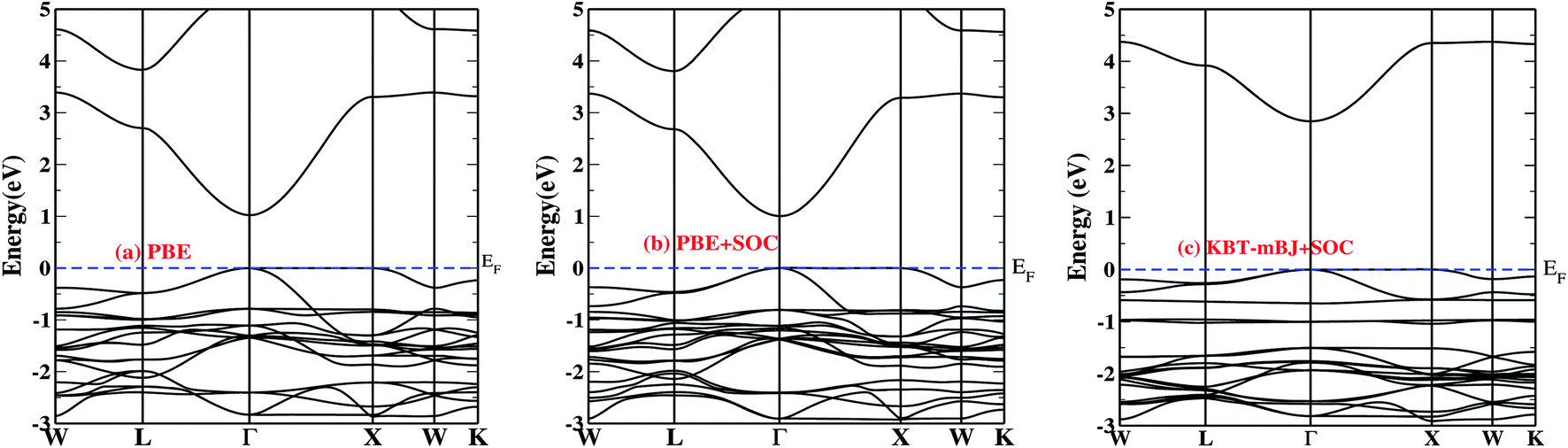 | ||
| Fig. 1 Electronic dispersion relations of Cs2InAgCl6 using: (a) PBE, (b) PBE + SOC, and (c) PBE with KTB-mBJ + SOC. The blue dashed lines represent the Fermi level (EF). | ||
Further information about the density of states (DOS) and projected DOS for the studied systems is given in Fig. SI-(2).†
To engineer the bandgap, we employed dual substitutional doping at different atomic sites, i.e., isoelectronic (K/Rb at the Cs site) and non-isoelectronic (Sn, Pb; Cu and Ga co-doping (CGCD)) doping.
For the isoelectronic doping we observed that, for the fully relaxed system, the lattice parameters changed less than 0.5% compared to the pristine case. Since K/Rb is doped in the cage of the octahedra (Cs-site) of AgCl6 and InCl6, their valence electron (ns1) is not expected to contribute near the VB/CB edges because it is located at the deep valence states near ∼6 eV. This was confirmed from the electronic structure calculations shown in Fig. SI-(3 and 4).† K(Rb) doping increases the bandgap by 0.18 (0.16 eV) compared to the pristine case due to the size effect of the dopant,45 and the band dispersion remains intact.
It has been reported46 that the band dispersion near the Fermi level can be altered significantly by alloying the octahedra cation site (Ag/In) to enhance the optoelectronic and opto-thermoelectric properties of the material. Therefore, we chose the Ag/In site for non-isoelectronic doping.
Fig. 2a and b depict the Pb- and Sn-doped band structures, respectively. Our findings reveal that Sn is a better dopant candidate compared to Pb for optoelectronic applications. A detailed description can be found in the next section.
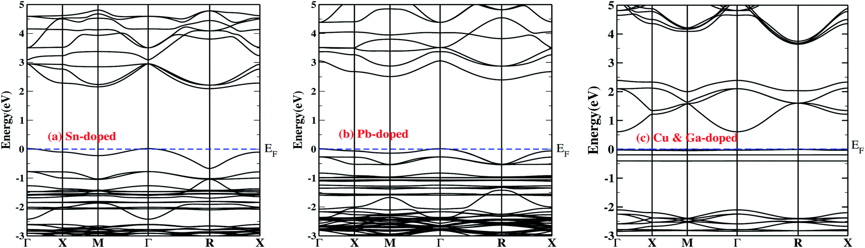 | ||
| Fig. 2 Electronic dispersion relations of: (a) 25% Sn-doped, (b) 25% Pb-doped, and (c) 12.5% Cu- and 12.5% Ga-doped Cs2InAgCl6 obtained using the PBE functional with the KTB-mBJ potential including the SO effect. The blue dashed lines represent the Fermi level. | ||
The doped system becomes an indirect semiconductor with a bandgap of 2.40 (2.08) eV after Pb(Sn) doping. The different reduction in the bandgap with Pb doping compared to Sn doping can be understood from the location of In-s states (Fig. 3), which is shifted by ∼0.3 eV when the system is doped with Pb rather than Sn. The VBM occurs at the Γ point, whereas in the conduction band there are two minima present at M and R. The minima in the conduction band are separated by ∼0.07 eV, which gives rise to the valley degeneracy responsible for the high figure of merit [ZT] for n-type carriers.47
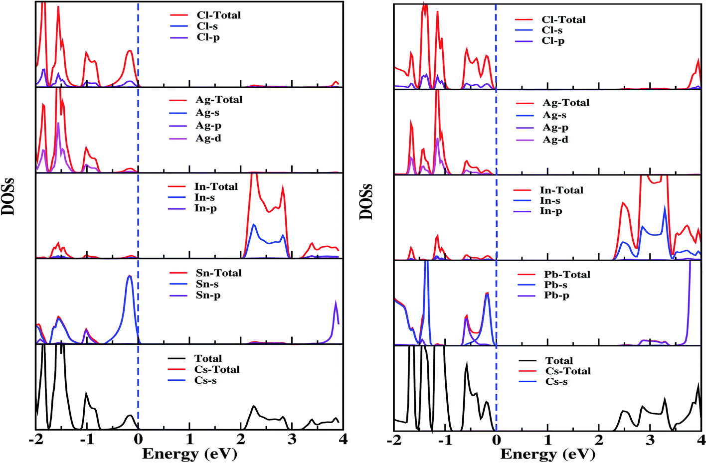 | ||
| Fig. 3 Calculated total, atom, and orbital decomposed densities of states of Sn- (left panel) and Pb- (right panel) doped Cs2InAgCl6 obtained using the PBE functional with the KTB-mBJ potential. | ||
Interestingly, we observed the presence of Sn/Pb-s states in the proximity of the Fermi level, giving rise to increased charge carriers, which are especially advantageous in the context of thermoelectrics.
Fig. 2c illustrates the band structure of the CGCD system. The top of the valence band is mainly composed of the Cu-d state with slight contributions from the In-s/p states. In the conduction band, the In-s state is shifted towards the Fermi level by ∼2.2 eV, reducing the bandgap value to 0.65 eV which is the lowest bandgap found among the various systems in the present study. The bandgap is indirect, which prevents fast electron–hole recombination, giving a high exciton lifetime.
The calculated total density of states of the studied alloys are illustrated in Fig. SI-(4 and 5; for K/Rb and CGCD†). In the next sections, we focus on the effects of the reduction of the bandgap on the optical and thermoelectric properties.
3.2. Optical properties
After calculating the Kohn–Sham (KS) electronic states using the k-grids mentioned in the crystal structure and computation methods section, we computed the optical absorption spectra using KTB-mBJ + SOC for pristine Cs2InAgCl6 along with its doped derivatives, which are shown in Fig. 4. A full description of the method and equations used in computing the optical properties is provided in ref. 41. The changes in the bandgap due to the substitutional dopants are clearly reflected in the optical spectra. For photovoltaic applications, a material must show high optical absorbance in the visible region of the solar spectrum.48,49 The optical absorption edge was calculated by extrapolation to be ∼2.80 eV for the pristine case, and gradually shifted towards lower energy with doping. For the CGCD system, the shift was drastic (See Fig. SI-6†).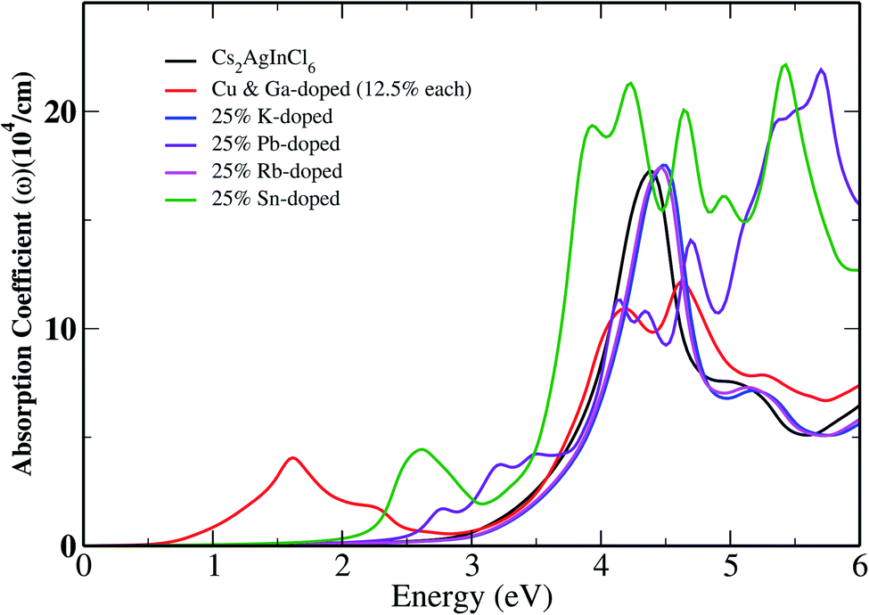 | ||
| Fig. 4 The absorption coefficient of Cs2InAgCl6 along with those of the doped cases as a function of the photon energy. | ||
Our results show that doping with a suitable candidate can significantly improve the optical absorption over the ultraviolet (UV) to IR (infrared) region. The optical absorption strength of the co-doped system in the IR solar spectrum region is stronger than that of the other doped systems, while in the visible region the Sn-doped system is dominant. The present findings may serve as a guide for experimental studies on these non-isoelectronic doped systems.
3.3. Thermoelectric properties
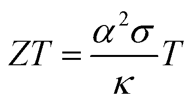
The thermoelectric (TE) transport properties were calculated using the linearized Boltzmann transport equation (BTE), as implemented in the BoltzTraP code,42 which solves the BTE within the constant relaxation time approximation (CRTA). The BoltzTraP code interpolates the band structure obtained from the DFT calculations, carries out the necessary integrations (Fermi integrals) at different temperatures and Fermi levels and provides the required transport coefficients as a function of temperature and carrier concentration (for both p-type and n-type); the results are shown in Fig. 5–7.The performance of a thermoelectric material is governed by the dimensionless figure of merit (ZT), which is given by50,51
Tuning the bandgap by substitutional doping changed the dispersion of the electronic bands around the Fermi level. This in turn governed the behavior of |α| and σ, and hence, the power factor was affected.
Fig. 5 depicts the Seebeck coefficient (|α|) for p-type and n-type pristine and doped systems. The isoelectronic doping (with K and Rb) (Fig. 5c and e) does not alter the |α| value, as there is no change in the dispersion of bands. We found that |α| shows typical behavior with decreasing carrier concentration, and also computed that the |α| value for the hole is higher than that for the electrons. Since |α| is directly proportional to the effective mass of the charge carriers, the flat band dispersion (Γ–X) at the valence band edges gives rise to a large hole effective mass  On the other hand, a parabolic band dispersion is observed for the conduction bands, leading to a lighter electron effective mass
  For the Pb/Sn-doped (Fig. 5d/f) system, the behavior of |α| can be interpreted based on the band gaps and band dispersion. For all temperatures, the |α| value of the electrons with the Pb-doped system is ∼3 times higher than that observed in the pristine case at n = 1020 cm−3, which was due to the downward shift of the In-s state. It was found that the Pb-doped system is more favorable than the pristine one. Moreover, we found that the |α| for the electrons exceeds that for the holes at higher carrier concentrations, the effect of which is reflected in the power factor (PF). In the case of CGCD, the narrow band gap triggers bipolar conduction at lower carrier concentrations, and due to the flat band, the electrical conductivity is too low compared to those of the other cases.
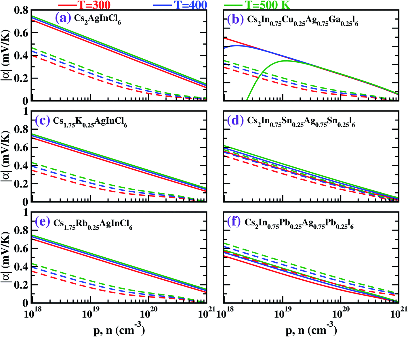 | ||
| Fig. 5 The carrier-concentration-dependent Seebeck coefficient (|α|) values at different temperatures for both p-type (solid) and n-type (dashed) (a) pristine, (b) Cu and Ga co-doped, (c) K-doped, (d) Sn-doped, (e) Rb-doped, and (f) Pb-doped Cs2AgInCl6. | ||
For all the cases, we obtained the electronic conductivity (σ) and PF by multiplying by τ = 10−14 s; this approach has also been adopted by others.42,52 The results are displayed in Fig. 6 and 7. We found that σ increases with increasing carrier concentration. In all the cases, σ was found to be greater for electrons than for holes due to the parabolic dispersion of the bands. However, in the Pb-doped system, the σ values for the electrons and holes were found to be of similar order, which is advantageous to boost performance with n-type doping.
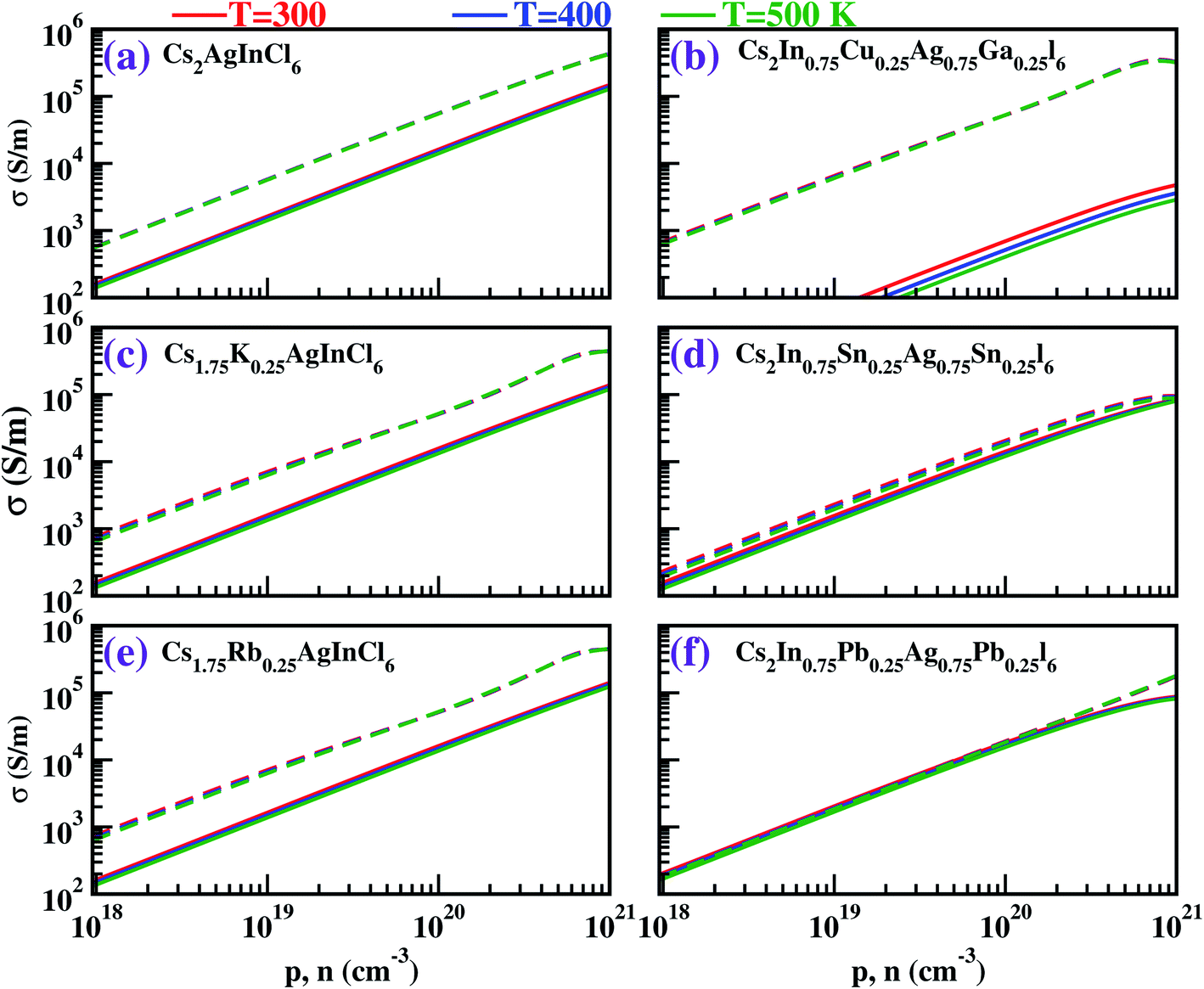 | ||
| Fig. 6 The electrical conductivity (σ) values at different temperatures for both p-type (solid) and n-type (dashed) (a) pristine, (b) Cu and Ga co-doped, (c) K-doped, (d) Sn-doped, (e) Rb-doped, and (f) Pb-doped Cs2AgInCl6. | ||
The temperature-dependent power factor, which is the product of α2 and σ, is plotted as a function of carrier concentration in Fig. 7. Because of the isoelectronic doping (Fig. 7c and e), the behavior of the power factor for the K-/Rb-doped cases is nearly the same as that for the pristine case with p-type doping, and slightly higher than that for the pristine case for n-type doping. For the co-doped case (Fig. 7b), the optimized value of the power factor with n-type doping is 0.6 mW m−1 K−2. A remarkable feature in our study is the significantly enhanced PF (2.03 mW m−1 K−2) for n-type carrier concentration for the Pb-doped case, in which the PF is ∼3.5 times higher than in the pristine case (0.6 mW m−1 K−2) at 500 K.
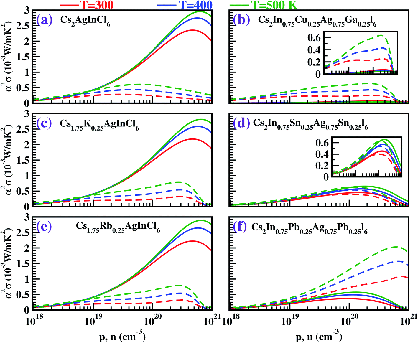 | ||
| Fig. 7 The power factor (α2σ) values at different temperatures for both p-type (solid) and n-type (dashed) (a) pristine, (b) Cu and Ga co-doped, (c) K-doped, (d) Sn-doped, (e) Rb-doped, and (f) Pb-doped Cs2AgInCl6. | ||
4. Conclusions
In summary, we studied the effects of K, Rb, and Cu–Ga/Pb/Sn substitution on the electronic, optical, and thermoelectric transport properties of Cs2InAgI6 using first-principles calculations. We found that K/Rb-substitution increases the bandgap slightly, while Cu–Ga/Pb/Sn-substitution decreases the band gap significantly. The studied K/Rb-based systems are direct bandgap semiconductors, while an indirect bandgap nature is observed for the other doped systems. The absorption peak is shifted from the ultraviolet region to the visible spectrum for the indirect bandgap compounds, but remains similar for the direct bandgap compounds. The optical absorption strength of the co-doped (Cu–Ga-based) system is stronger than that of the other doped systems in the IR solar region, while in the visible region, the Sn-doped system shows dominant absorption. Significant changes in thermoelectric properties were noted in the Pb- and co-doped cases. The flat valence bands are responsible for the poor thermoelectric performance of the co-doped system. The downward shift of the In-s state in the Pb-doped system enhances the PF ∼3.5-fold compared to the pristine case (0.6 mW m−1 K−2) at 500 K with n-type doping. Thus, our investigation reveals that the Pb-doped system is a promising candidate for thermoelectric applications.Conflicts of interest
There are no conflicts to declare.Acknowledgements
KCB and CSP acknowledge DST and DST-SERB for SERB-NPDF and INSPIRE Faculty fellowships with award numbers IFA-18 PH217 and PDF/2017/002876, respectively. The research used resources at the National Energy Research Scientific Computing Center (NERSC), which is supported by the Office of Science of the USDOE, United States, under contract no. DE-AC02-05CH11231. The high-performance computational facility of the Centre for Development of Advanced Computing, Pune, was also used for the present investigation.References
- C. R. Lhermitte and K. Sivula, ACS Catal., 2019, 9, 2007–2017 CrossRef CAS.
- P. Bermel, K. Yazawa, J. L. Gray, X. Xu and A. Shakouri, Energy Environ. Sci., 2016, 9, 2776–2788 RSC.
- S. Hirotsu, J. Harada, M. Iizumi and K. Gesi, J. Phys. Soc. Jpn., 1974, 37, 1393–1398 CrossRef CAS.
- A. Kojima, K. Teshima, Y. Shirai and T. Miyasaka, J. Am. Chem. Soc., 2009, 131, 6050–6051 CrossRef CAS PubMed.
- M. M. Lee, J. Teuscher, T. Miyasaka, T. N. Murakami and H. J. Snaith, Science, 2012, 338, 643–647 CrossRef CAS PubMed.
- M. Neukom, S. Züfle, S. Jenatsch and B. Ruhstaller, Sci. Technol. Adv. Mater., 2018, 19, 291–316 CrossRef CAS PubMed.
- G. Grancini, C. Roldán-Carmona, I. Zimmermann, E. Mosconi, X. Lee, D. Martineau, S. Narbey, F. Oswald, F. De Angelis, M. Graetzel and others, Nat. Commun., 2017, 8, 15684 CrossRef CAS PubMed.
- F. F. Targhi, Y. S. Jalili and F. Kanjouri, Results Phys., 2018, 10, 616–627 CrossRef.
- N. Hernández-Haro, J. Ortega-Castro, Y. B. Martynov, R. G. Nazmitdinov and A. Frontera, Chem. Phys., 2019, 516, 225–231 CrossRef.
- G. Giorgi, J.-I. Fujisawa, H. Segawa and K. Yamashita, J. Phys. Chem. C, 2014, 118, 12176–12183 CrossRef CAS.
- P. Umari, E. Mosconi and F. De Angelis, Sci. Rep., 2014, 4, 4467 CrossRef PubMed.
- S.-Y. Yue, X. Zhang, G. Qin, J. Yang and M. Hu, Phys. Rev. B: Condens. Matter Mater. Phys., 2016, 94, 115427 CrossRef.
- X. Qian, X. Gu and R. Yang, Appl. Phys. Lett., 2016, 108, 63902 CrossRef.
- T. Zhao, D. Wang and Z. Shuai, Synth. Met., 2017, 225, 108–114 CrossRef CAS.
- Y.-Y. Zhang, S. Chen, P. Xu, H. Xiang, X.-G. Gong, A. Walsh and S.-H. Wei, Chin. Phys. Lett., 2018, 35, 36104 CrossRef.
- Z. Li, Q. Xu, Q. Sun, Z. Hou and W.-J. Yin, Adv. Funct. Mater., 2019, 29, 1807280 CrossRef.
- Q. Fu, X. Tang, B. Huang, T. Hu, L. Tan, L. Chen and Y. Chen, Adv. Sci., 2018, 5, 1700387 CrossRef PubMed.
- F. Wei, Z. Deng, S. Sun, F. Xie, G. Kieslich, D. M. Evans, M. A. Carpenter, P. D. Bristowe and A. K. Cheetham, Mater. Horiz., 2016, 3, 328–332 RSC.
- F. Wei, Z. Deng, S. Sun, F. Zhang, D. M. Evans, G. Kieslich, S. Tominaka, M. A. Carpenter, J. Zhang, P. D. Bristowe and others, Chem. Mater., 2017, 29, 1089–1094 CrossRef CAS.
- Z. Deng, F. Wei, S. Sun, G. Kieslich, A. K. Cheetham and P. D. Bristowe, J. Mater. Chem. A, 2016, 4, 12025–12029 RSC.
- F. Giustino and H. J. Snaith, ACS Energy Lett., 2016, 1, 1233–1240 CrossRef CAS.
- X.-G. Zhao, J.-H. Yang, Y. Fu, D. Yang, Q. Xu, L. Yu, S.-H. Wei and L. Zhang, J. Am. Chem. Soc., 2017, 139, 2630–2638 CrossRef CAS PubMed.
- A. H. Slavney, T. Hu, A. M. Lindenberg and H. I. Karunadasa, J. Am. Chem. Soc., 2016, 138, 2138–2141 CrossRef CAS PubMed.
- A. Jain, O. Voznyy and E. H. Sargent, J. Phys. Chem. C, 2017, 121, 7183–7187 CrossRef CAS.
- E. T. McClure, M. R. Ball, W. Windl and P. M. Woodward, Chem. Mater., 2016, 28, 1348–1354 CrossRef CAS.
- L. Chu, W. Ahmad, W. Liu, J. Yang, R. Zhang, Y. Sun, J. Yang and others, Nano-Micro Lett., 2019, 11, 16 CrossRef PubMed.
- Z. Xiao, W. Meng, J. Wang and Y. Yan, ChemSusChem, 2016, 9, 2628–2633 CrossRef CAS PubMed.
- C. N. Savory, A. Walsh and D. O. Scanlon, ACS Energy Lett., 2016, 1, 949–955 CrossRef CAS PubMed.
- D. Han, T. Zhang, M. Huang, D. Sun, M.-H. Du and S. Chen, APL Mater., 2018, 6, 84902 CrossRef.
- G. Volonakis, A. A. Haghighirad, R. L. Milot, W. H. Sio, M. R. Filip, B. Wenger, M. B. Johnston, L. M. Herz, H. J. Snaith and F. Giustino, J. Phys. Chem. Lett., 2017, 8, 772–778 CrossRef CAS PubMed.
- J. Sun and D. J. Singh, J. Mater. Chem. A, 2017, 5, 8499–8509 RSC.
- P. Blaha, K. Schwarz, F. Tran, R. Laskowski, G. K. H. Madsen and L. D. Marks, J. Chem. Phys., 2020, 152, 74101 CrossRef CAS PubMed.
- P. Blaha, K. Schwarz, G. K. H. Madsen, D. Kvasnicka, J. Luitz, R. Laskowski, F. Tran and L. D. Marks, WIEN2k, An Augmented Plane Wave + Local Orbitals Program for Calculating Crystal Properties, Karlheinz Schwarz, Techn. Universität Wien, Austria, 2018, ISBN 3-9501031-1-2 Search PubMed.
- J. P. Perdew, K. Burke and M. Ernzerhof, Phys. Rev. Lett., 1996, 77, 3865 CrossRef CAS PubMed.
- J. P. Perdew, A. Ruzsinszky, G. I. Csonka, O. A. Vydrov, G. E. Scuseria, L. A. Constantin, X. Zhou and K. Burke, Phys. Rev. Lett., 2008, 100, 136406 CrossRef PubMed.
- F. Tran and P. Blaha, Phys. Rev. Lett., 2009, 102, 226401 CrossRef PubMed.
- D. Koller, F. Tran and P. Blaha, Phys. Rev. B: Condens. Matter Mater. Phys., 2012, 85, 1–10 Search PubMed.
- A. D. Becke and E. R. Johnson, J. Chem. Phys., 2006, 124, 221101 CrossRef PubMed.
- D. Koller, F. Tran and P. Blaha, Phys. Rev. B: Condens. Matter Mater. Phys., 2011, 83, 195134 CrossRef.
- R. A. Jishi, O. B. Ta and A. A. Sharif, J. Phys. Chem. C, 2014, 118, 28344–28349 CrossRef CAS.
- C. Ambrosch-Draxl and J. O. Sofo, Comput. Phys. Commun., 2006, 175, 1–14 CrossRef CAS.
- G. K. H. Madsen and D. J. Singh, Comput. Phys. Commun., 2006, 175, 67–71 CrossRef CAS.
- J. Sun and D. J. Singh, Phys. Rev. Appl., 2016, 5, 24006 CrossRef.
- E. Haque and M. A. Hossain, Comput. Condens. Matter, 2019, 19, e00374 CrossRef.
- K. C. Bhamu, A. Soni and J. Sahariya, Sol. Energy, 2018, 162, 336–343 CrossRef CAS.
- P. Zhang, J. Yang and S.-H. Wei, J. Mater. Chem. A, 2018, 6, 1809–1815 RSC.
- M. Mukherjee, G. Yumnam and A. K. Singh, J. Phys. Chem. C, 2018, 122, 29150–29157 CrossRef CAS.
- C. Brabec, U. Scherf and V. Dyakonov, Organic photovoltaics: materials, device physics, and manufacturing technologies, John Wiley & Sons, 2011 Search PubMed.
- E. Rephaeli and S. Fan, Opt. Express, 2009, 17, 15145–15159 CrossRef CAS PubMed.
- A. Ioffe, Semiconductor Thermoelements and Thermoelectric Cooling, Infosearch, London, 1st edn, 1957 Search PubMed.
- H. J. Goldsmid, Introduction to thermoelectricity, Springer, 2010, vol. 121 Search PubMed.
- S.-D. Guo, J. Mater. Chem. C, 2016, 4, 9366–9374 RSC.
Footnotes |
| † Electronic supplementary information (ESI) available. See DOI: 10.1039/d0ra01840f |
| ‡ Author contributed equally to the work. |
| This journal is © The Royal Society of Chemistry 2021 |