
 Open Access Article
 This Open Access Article is licensed under a Creative Commons Attribution-Non Commercial 3.0 Unported Licence
Significant enhancement in quantum-dot light emitting device stability via a ZnO:polyethylenimine mixture in the electron transport layer†
Dong Seob
Chung
 a,
Tyler
Davidson-Hall
a,
Hyeonghwa
Yu
a,
Fatemeh
Samaeifar
a,
Peter
Chun
b,
Quan
Lyu
c,
Giovanni
Cotella
c and
Hany
Aziz
*a
a,
Tyler
Davidson-Hall
a,
Hyeonghwa
Yu
a,
Fatemeh
Samaeifar
a,
Peter
Chun
b,
Quan
Lyu
c,
Giovanni
Cotella
c and
Hany
Aziz
*a
aDepartment of Electrical and Computer Engineering and Waterloo Institute for Nanotechnology, University of Waterloo, 200 University Avenue West, Waterloo, Ontario N2L 3G1, Canada. E-mail: h2aziz@uwaterloo.ca
bOttawa IC Laboratory, Huawei Canada, 19 Allstate Parkway, Markham, ON L3R 5B4, Canada
cIpswich Research Centre, Huawei Technologies Research & Development (UK) Ltd., Phoenix House (B55), Adastral Park, Ipswich IP5 3RE, UK
First published on 17th August 2021
Abstract
The effect of adding polyethylenimine (PEI) into the ZnO electron transport layer (ETL) of inverted quantum dot (QD) light emitting devices (QDLEDs) to form a blended ZnO:PEI ETL instead of using it in a separate layer in a bilayer ZnO/PEI ETL is investigated. Results show that while both ZnO/PEI bilayer ETL and ZnO:PEI blended ETL can improve device efficiency by more than 50% compared to QDLEDs with only ZnO, the ZnO:PEI ETL significantly improves device stability, leading to more than 10 times longer device lifetime. Investigations using devices with marking luminescent layers, electron-only devices and delayed electroluminescence measurements show that the ZnO:PEI ETL leads to a deeper penetration of electrons into the hole transport layer (HTL) of the QDLEDs. The results suggest that the stability enhancement may be due to a consequent reduction in hole accumulation at the QD/HTL interface. The findings show that ZnO:PEI ETLs can be used for enhancing both the efficiency and stability of QDLEDs. They also provide new insights into the importance of managing charge distribution in the charge transport layers for realizing high stability QDLEDs and new approaches to achieve that.
Introduction
Owing to their unique luminescence properties, which include high quantum yield, narrow emission spectra and size-dependent colour tunability, colloidal quantum dot (QD) materials are attracting significant attention of the scientific community for utilization in future optoelectronic and energy harvesting devices.1–7 Electroluminescent quantum dot light emitting devices (QDLEDs) are emerging as forefront players for next generation flat panel displays. With high electroluminescence (EL) efficiency and stability, in some cases reaching an external quantum efficiency (EQE) of 30.9%8 and an LT95 of 11![[thin space (1/6-em)]](https://www.rsc.org/images/entities/char_2009.gif) 000 hours from an initial luminance (L0) of 1000 cd m−2,9 the performance of these devices is quickly approaching that of organic light emitting devices (OLEDs) used in commercial products. Despite this remarkable progress, the EL stability of many QDLEDs remains relatively low, and the root causes of this behaviour are still not well understood.9–14 While early work has focused primarily on the QD light emission layer (EML) for understanding the root causes of this phenomenon,17 recent findings show that the charge transport layers also play a major role in their EL stability.15–17 This is especially true for the hole transport layers (HTLs) which comprise organic materials and thus have high propensity to degradation by excitons, thermal and environmental stress factors.11,18–20 In these devices the electron transport layers (ETLs) are commonly made of ZnO due to its chemical stability, high electron mobility and the energy of its conduction band which well matches that of the QDs and thus facilitates electron injection into the QD EML. Solution-coated ZnO ETLs however have structural and stoichiometric defects that can act as exciton quenching sites and thereby reduce device EQE.21,22 Therefore, to passivate the ZnO surface and/or prevent excitons from reaching it a thin layer of a wide bandgap material, such as Al2O3 (ref. 13) or a polymeric material,22–26 is often introduced in between the ZnO ETL and the EML. Polymers containing aliphatic amine groups, such as polyethylenimine (PEI) and its ethoxylated derivative (PEIE), are often used for this purpose.27,28 These polymers have been used as electrode interfacial layers in OLEDs and organic solar cells (OSCs) in recent years for facilitating electron injection. The efficiency enhancement observed upon their use as ZnO passivation layers in QDLEDs is therefore sometimes also attributed to a similar effect. However, since electron injection into the QDs is already asymmetrically higher than hole injection, an improvement in electron injection should worsen rather than improve charge balance in the EML and thus reduce EQE. Alternative explanations for the efficiency enhancement have therefore been provided, focusing on the role of PEI(E) in passivating the ZnO surface,28 shifting the electron–hole recombination zone away from the QD/HTL interface21 or impeding (rather than facilitating) electron supply to the QD EML due to its insulating nature.27 Conversely, while the influence of PEI passivation layers on QDLED efficiency has been well studied, their impact on stability has received much less attention, with only one recent study suggesting that they had a limited effect.21 They also need to be used in the form of ultrathin (<10 nm), pin-hole free layers which is challenging for solution coating. Instead, mixing the PEI into the ZnO in the form of a ZnO:PEI blended ETL instead of a separate layer has therefore been recently proposed,29 similar to what was done in OLEDs29–31 and OSCs.32–36 In the only report applying a ZnO:PEI(E) ETL to QDLEDs, Shi et al. showed that using a ZnO:PEIE blended ETL can improve the efficiency of inverted blue QDLEDs but its effect on stability was not addressed.37
000 hours from an initial luminance (L0) of 1000 cd m−2,9 the performance of these devices is quickly approaching that of organic light emitting devices (OLEDs) used in commercial products. Despite this remarkable progress, the EL stability of many QDLEDs remains relatively low, and the root causes of this behaviour are still not well understood.9–14 While early work has focused primarily on the QD light emission layer (EML) for understanding the root causes of this phenomenon,17 recent findings show that the charge transport layers also play a major role in their EL stability.15–17 This is especially true for the hole transport layers (HTLs) which comprise organic materials and thus have high propensity to degradation by excitons, thermal and environmental stress factors.11,18–20 In these devices the electron transport layers (ETLs) are commonly made of ZnO due to its chemical stability, high electron mobility and the energy of its conduction band which well matches that of the QDs and thus facilitates electron injection into the QD EML. Solution-coated ZnO ETLs however have structural and stoichiometric defects that can act as exciton quenching sites and thereby reduce device EQE.21,22 Therefore, to passivate the ZnO surface and/or prevent excitons from reaching it a thin layer of a wide bandgap material, such as Al2O3 (ref. 13) or a polymeric material,22–26 is often introduced in between the ZnO ETL and the EML. Polymers containing aliphatic amine groups, such as polyethylenimine (PEI) and its ethoxylated derivative (PEIE), are often used for this purpose.27,28 These polymers have been used as electrode interfacial layers in OLEDs and organic solar cells (OSCs) in recent years for facilitating electron injection. The efficiency enhancement observed upon their use as ZnO passivation layers in QDLEDs is therefore sometimes also attributed to a similar effect. However, since electron injection into the QDs is already asymmetrically higher than hole injection, an improvement in electron injection should worsen rather than improve charge balance in the EML and thus reduce EQE. Alternative explanations for the efficiency enhancement have therefore been provided, focusing on the role of PEI(E) in passivating the ZnO surface,28 shifting the electron–hole recombination zone away from the QD/HTL interface21 or impeding (rather than facilitating) electron supply to the QD EML due to its insulating nature.27 Conversely, while the influence of PEI passivation layers on QDLED efficiency has been well studied, their impact on stability has received much less attention, with only one recent study suggesting that they had a limited effect.21 They also need to be used in the form of ultrathin (<10 nm), pin-hole free layers which is challenging for solution coating. Instead, mixing the PEI into the ZnO in the form of a ZnO:PEI blended ETL instead of a separate layer has therefore been recently proposed,29 similar to what was done in OLEDs29–31 and OSCs.32–36 In the only report applying a ZnO:PEI(E) ETL to QDLEDs, Shi et al. showed that using a ZnO:PEIE blended ETL can improve the efficiency of inverted blue QDLEDs but its effect on stability was not addressed.37
In this work, we investigate and compare between using ZnO:PEI blended ETL and a bilayer ZnO/PEI ETL structure on device performance in inverted red QDLEDs. Results indicate that while both ZnO/PEI bilayer ETL and ZnO:PEI blended ETL can improve device efficiency by more than 50% compared to QDLED with the ZnO ETL, the ZnO:PEI ETL has a significant advantage in terms of improving device stability, leading to more than 10 times longer LT50, defined as time elapsed before the luminance decreases to 50% of its initial value, in the case of ZnO:PEI ETL with 0.3 wt% PEI. Investigations show that the ETL enables a deeper penetration of electrons into the HTL, suggesting that the stability enhancement may be the result of a consequent reduction in hole accumulation in the HTL at the QD/HTL interface, the latter being a known cause of the deterioration in EQE over time.38
Experimental section
Device fabrication
Inverted QDLEDs of the structure ITO/ETL/QD/CBP/MoO3/Al are used in this work. Indium tin oxide (ITO) patterned glass substrates from Kintec are first sonicated with Micro 90 and DI water, and then sequentially rinsed with acetone and isopropanol. The washed substrates are then treated by an oxygen plasma to improve the wettability of the ITO surface. Zinc acetate (197 mg, Sigma-Aldrich) and ethanolamine (54 μL, Sigma-Aldrich) are mixed in ethanol (6 mL, Sigma-Aldrich) on a 50 °C hotplate with vigorous stirring at 700 rpm for 40 minutes in a N2 filled glove box for sol–gel ZnO. PEI solution is prepared by stirring branched-PEI (Sigma-Aldrich) in ethanol or 1-propanol (Sigma-Aldrich) at 700 rpm overnight in a N2 filled glove box. 1 mL of PEI solutions in ethanol with different concentrations are then mixed with 1 mL of ZnO solution at 700 rpm for 1 hour to make solutions of the different ZnO:PEI ratios. ZnO solutions are spin coated at 1000 rpm on the cleaned ITO substrates followed by 150 °C baking on a hotplate for 30 minutes. ZnO:PEI blended solution is deposited by solution coating at 2000 rpm followed by 120 °C baking on a hotplate for 30 minutes. For the ZnO/PEI bilayer ETL, 0.5 mg mL−1 of PEI dissolved in 1-propanol is spin coated at 5000 rpm followed by 120 °C baking on a hotplate for 20 minutes on top of a ZnO film. 4 mg mL−1 CdZnSe/ZnSe/CdZnS/ZnSQDs (Mesolight Inc.) dispersed in octane (Sigma-Aldrich) is deposited on the ETL at 500 rpm and baked on a 50 °C hotplate for 30 minutes. 4,4′-Bis(N-carbazolyl)-1,1′-biphenyl (CBP, Angstrom Engineering), molybdenum trioxide (MoO3, Angstrom Engineering) and aluminium (Al, Angstrom Engineering) are then deposited using a thermal evaporator (Angstrom Engineering) at 5 × 10⁻⁶ torr for HTL, hole injection layer (HIL) and anode. Film thicknesses are measured using a Dektak-150 profilometer.
Device characterization
Current–voltage–luminance (J–V–L) measurements are conducted using an Agilent 4155C semiconductor parameter analyzer with a silicon photodiode and a Minolta CS-100 Chromameter. EL and PL spectra are collected using an Ocean Optics QE65000 spectrometer, using a Newport 67005 200 W HgXe arc lamp with a monochromator as a PL excitation source. Device EL stability measurements are conducted under a constant current of 20 mA cm−2 using an M6000PLUS OLED lifetime test system. Surface topography measurements are conducted using a Veeco Nanoscope atomic force microscope (AFM). Time-resolved photoluminescence (TRPL) is measured using an Edinburgh Instruments FL920 spectrometer. Delayed electroluminescence is measured with an R928 photomultiplier tube and the signal is amplified using a Keithley 428 current amplifier. The prompt EL signal is blocked with the help of a ThorLabs MC1000A optical chopper. Forward and reverse bias pulse signals are applied using a Stanford Research Systems DG535 digital delay/pulse generator. A Tectronix TDS5054 digital phosphor oscilloscope then records the delayed EL signals. The QDLEDs are kept in a nitrogen atmosphere at all times.
Results and discussion
We first compare the effect of using a ZnO:PEI blended ETL vs. a ZnO/PEI bilayer ETL vs. a ZnO-only ETL on the EL characteristics of the QDLEDs. For this purpose we fabricate and test four groups of QDLEDs of the general structure ITO/ETL (∼32 nm)/QD (30 nm)/CBP (50 nm)/MoO3 (5 nm)/Al, with the ETL made of ZnO:PEI with 0.1% or 0.3% PEI by weight (we will denote ZnO:ETL with different concentrations 0.1 wt% and 0.3 wt% as ZnO:PEI0.1 and ZnO:PEI0.3, respectively), ZnO/PEI or only ZnO, the last one to serve as control. The thickness of the ETL in all devices was ∼32 (±3 nm), which included the additional thickness of the neat PEI layer (∼8 nm) in the case of the bilayer ETL. Fig. 1(a) depicts the general QDLED structure, whereas Fig. 1(b, c and d) present the JVL, EQE and EL spectra of the devices, respectively. As can be seen from the J–V characteristics, the devices with the ZnO/PEI and ZnO:PEI ETLs all have a higher threshold voltage (Vth) and a lower current density at any given voltage in comparison to the control device.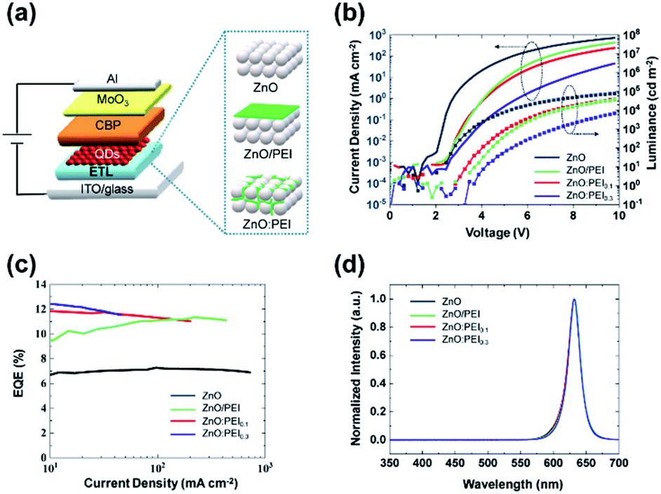 | ||
| Fig. 1 (a) Schematic diagram showing the general structure of the QDLEDs and the different ETLs investigated in this work. (b) J–V–L characteristics, (c) EQE, and (d) electroluminescence spectra of the QDLEDs. | ||
One can also see that increasing the PEI concentration from 0.1 wt% to 0.3 wt% in the ZnO:PEI ETL reduces the current at any given voltage. The higher Vth and lower current density suggest that the PEI makes electron injection and transport more difficult, an effect that can be attributed to its low conductivity. An examination of the EQE vs. current density characteristics in Fig. 1(c) shows that using the PEI brings about a significant increase in EQE, increasing the maximum value from 7.7% (in the case of the ZnO control device) to 11.2%, 11.0% and 12.1% for the ZnO/PEI, ZnO:PEI0.1, and ZnO:PEI0.3 devices, respectively. With the J–V characteristics in perspective, the EQE enhancement can be attributed, at least in part, to the role of the PEI in reducing the charge imbalance in the QD EML produced by the asymmetric carrier injection barriers. The passivation of ZnO surface defects by the PEI may also be contributing to this efficiency enhancement. While this passivation effect has only been studied in devices with ZnO/PEI in the past,24 we may expect a similar effect in the case of the ZnO:PEI blends. The EL spectra (Fig. 1(d)) show a single emission band with a peak at wavelength 632 nm, indicating that the majority of radiative recombination happens in the QD EML in all devices.
To test the passivation effect of PEI of ZnO surface states, we use TRPL measurements to probe changes in the QD exciton lifetime on the various ETLs. Because ZnO surface defects act as efficient quenching sites for QD excitons, their passivation would extend the exciton lifetime and lead to a slower decay in the TRPL characteristics of the QDs in contact with the ETL. Fig. 2 depicts the TRPL characteristics of the QD layers on the four ETL configurations, collected at a wavelength of 630 nm (i.e. the QD emission peak). Clearly, the TRPL decay rates depend on the ETL, with QDs coated on ZnO/PEI exhibiting the slowest decay rate and those coated on ZnO exhibiting the fastest decay rate. The slow decay rate in the case of the ZnO/PEI points to the effectiveness of the PEI layer in passivating the ZnO surface defects, consistent with previous reports.21,24,37 The slower decay rate of the ZnO:PEI samples relative to the ZnO control indicates that mixing PEI into the ZnO also confers some surface passivation effect although to a lesser extent in comparison to the case where the ZnO surface is covered completely by a PEI layer. Notably, increasing the PEI concentration in the ZnO:PEI layer from 0.1% to 0.6% ZnO:PEI is found to have a negligible effect on the TRPL decay rate (see Fig. S1†), suggesting that the passivation effect of PEI in the ZnO:PEI blends quickly reaches saturation. These results therefore verify that a reduction in exciton quenching at the ZnO/QD interface contributes to the higher EQE of the ZnO/PEI and ZnO:PEI devices. The similar EQE enhancement with both types of ETLs (i.e. ZnO/PEI and ZnO:PEI) despite the different extents of passivation by the PEI in the two cases however suggests that the surface passivation is not the leading factor behind the EQE enhancement.
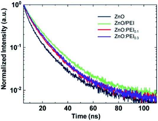 | ||
| Fig. 2 TRPL characteristics of the QDs on ZnO, ZnO/PEI, ZnO:PEI0.1 and ZnO:PEI0.3. | ||
Next, we test the EL stability of the devices under constant current driving at 20 mA cm−2. Fig. 3(a and b) show the normalized luminance (relative to the initial luminance, L0) and changes in the driving voltage (driving voltage at time, t, minus the initial driving voltage) vs. time plots of the devices, respectively. The LT50 of the ZnO ETL and ZnO/PEI devices is 46 hours and 62 hours, respectively (from an L0 of 2500 and 3030 cd m−2, respectively). In contrast, the LT50 of the ZnO:PEI devices is markedly longer, amounting to 140 hours in the case of the ZnO:PEI0.1 device and 292 hours in the case of the ZnO:PEI0.3 device (from an L0 of 3000 and 3250 cd m−2, respectively). Using the lifetime scaling rule (L0nLT50 = constant) and the widely used value of 1.8 for the scaling coefficient,39 these values correspond to LT50 values of 15100 hours, 28773 hours, 65630 hours and 153735 hours, respectively for an L0 of 100 cd m−2. Introducing the PEI into the ZnO layer instead of having it in a separate layer leads to a significant enhancement in the EL stability of QDLEDs, leading to ∼10 times longer LT50 at L0 of 100 cd m−2. Table S1† summarizes the LT50 values of the devices and their EQEs. There is a distinct difference between the trends of the control device and the PEI containing devices in the driving voltage trends of Fig. 3(b), with the latter experiencing an initial decrease in the driving voltage before beginning to rise over time. In general, an increase in driving voltage during electrical driving can be attributed to the formation of space charges within the device layers that create internal electric fields of opposite direction to the field produced by the external bias which require an increase of the external bias to offset their effect and maintain the same current flow. As the difficulty of injecting holes into the QD EML arising from the large energy difference between the HOMO of the HTL and the valence band of the QD is a bottleneck for current flow in QDLEDs in general, one can expect the increase in voltage to be associated with hole accumulation and the build-up of hole space charges in the HTL near the HTL/QD interface.10,40 The fact that the presence of the PEI alters the trend of the driving voltage initially therefore suggests that it may be slowing down the formation of these hole space charges. One also notes the different curvatures (i.e. trajectory) of the driving voltage trends of the PEI devices where the increase in voltage seems to accelerate in the longer term. Surprisingly this effect seems to be most significant in the case of ZnO:PEI0.3 which exhibits the fastest increase in driving voltage despite it having the highest EL stability. That this increase in driving voltage does not seem to negatively affect device efficiency (as inferred from the stable EL) suggests that it may be arising from space charges that are formed far away from the QD EML.
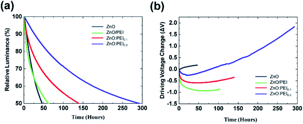 | ||
| Fig. 3 Relative luminance (a) and changes in driving voltage (b) vs. time trends of the QDLEDs with the different ETLs under 20 mA cm−2 constant current driving conditions. | ||
In order to investigate the root causes of the stability enhancement we first investigate the surface topography of the ETLs. Since in inverted devices the QD EML is coated on the ETL, differences in ETL surface topography or roughness may influence the morphological uniformity of the EML or subsequent layers and thus affect device stability. Therefore AFM scans were conducted on 32 nm thick films of ZnO, ZnO/PEI of ZnO:PEI coated on ITO glass substrates. The images are shown in Fig. 4(a–d). The surface topographies of the ETLs are very similar and roughness measurements indicate that all films have very smooth surfaces. The root-mean-square surface roughness (Rq) for the ZnO and ZnO/PEI was 1.360 nm and 1.098 nm, respectively. This is consistent with previous studies showing that coating PEI on ZnO brings about some surface planarization effect.28 The Rq of ZnO:PEI0.1 and ZnO:PEI0.3 films were slightly lower than the ZnO control, with 1.106 nm and 1.271 nm, respectively. Their homogeneous morphology and similarity to that of the ZnO control suggest that the PEI is well dispersed in the ZnO matrix. This is consistent with the TRPL results that show that introducing even a small amount of PEI affects the TRPL decay rates which indicates that the PEI is effective in passivating a significant fraction of ZnO surface defects and points to strong interactions between the two materials and hence good dispersion. The very similar morphology and surface roughness of all ETLs, however, indicates that surface roughness modification by PEI cannot be the main source of the device stability enhancement in the case of the ZnO:PEI devices.
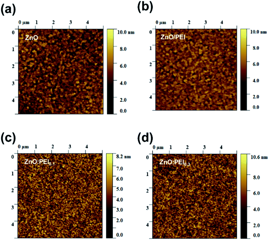 | ||
| Fig. 4 AFM surface topography images of (a) ZnO, (b) ZnO/PEI, (c) ZnO:PEI0.1, and (d) ZnO:PEI0.3. | ||
Finding that morphological factors are unlikely to cause the EL stability enhancement of the ZnO:PEI ETL devices and that the use of PEI in the ETLs significantly affects both the J–V characteristics (Fig. 1(b)) and the increase in driving voltage over time (Fig. 3(b)), we investigate if the ETLs affect the electron–hole recombination zone or otherwise alter the distribution of electrons and holes in the HTL. We therefore fabricate devices that contain a thin luminescent marking layer in the HTL which will emit light if excitons are created nearby. The 10 nm marking layer consisted of 10% bis[2-(4,6-difluorophenyl)pyridinato-C2,N] (picolinato) iridium(III) (FIrpic) by volume doped into the CBP HTL. FIrpic is selected because of its comparable energy band structure to CBP which minimizes altering charge distribution from that in the original devices. In addition, its high quantum yield and luminescence in the 450–550 nm range, far from the QD emission band (at 632 nm), make it relatively easy to distinguish its EL. The marking layer was placed 10 nm away from the QD/HTL interface in order to avoid quenching FIrpic via energy transfer to the QD layer.41 The general device structure of these devices therefore is: ITO/ETLs/QD/CBP (10 nm)/CBP:FIrpic (10 nm)/CBP (30 nm)/MoO3 (5 nm)/Al (100 nm). Fig. 5(a) shows the general device structure whereas Fig. 5(b) shows the EL spectra measured from QDLEDs incorporating the different ETLs while driven at 20 mA cm−2 current density. The spectrum of a ZnO device without a marking layer is also included for comparison. All the spectra are normalized to the QD emission band peak intensity to facilitate comparison. The ZnO:PEI devices show significant emission from the FIrpic marking layer indicating that a significant number of electrons can penetrate into the HTL and reach the marking layer where they recombine with holes to produce EL. In stark contrast, the spectrum of the ZnO/PEI device shows only very weak (but discernible) emission from FIrpic, indicating that the penetration of electrons into the HTL is much less in this case. The ZnO device shows no detectable FIrpic emission, evident from the comparable background noise to that of the control device without the marking layer over the 450–550 nm range. For any given current density a higher electron current requires that the hole current must be proportionally lower at the same device cross-sectional plane indicating that hole currents must be somewhat lower in the HTL near the QD interface in the case of the ZnO:ETL devices. A deeper penetration of electrons into the HTL also points to a lower concentration of accumulated holes in the HTL at the QD/HTL interface, otherwise the electrons would have been annihilated (i.e. neutralized) by recombination with these holes. The fact that this effect is strongest in the case of the ZnO:PEI devices and that these devices also exhibit a significantly higher EL stability suggests that there is a correlation between the two phenomena. In this regard the higher stability is possibly associated with a lower concentration of holes in the HTL at the QD/HTL interface whose presence in high concentrations would otherwise reduce the luminescence of the QD EML by Auger quenching or by degrading the HTL in the vicinity of the HTL/QD by excitons.38 This effect is schematically illustrated in Fig. S4.† While the deeper penetration of electrons into the HTL in the case of the ZnO:PEI devices may seem inconsistent at first glance with the shifts in the J–V characteristics which suggest that these ETLs make electron injection and transport more difficult, it is possible that restricting the electron supply leads to higher internal electric fields within the device that facilitate hole injection from the HTL into the QD layer and/or the penetration of electrons into the HTL, either of which would reduce hole accumulation in the HTL at the QD/HTL interface. For example, reducing the number of electrons in the QD layer would be expected to lead to a higher electric field across it which may help energy band bending at the QD/HTL interface and facilitate hole injection. The increased hole injection may, in turn, reduce the hole space charges at the QD/HTL interface leading to a higher electric field across the HTL that can help electrons to penetrate into it. Indeed, increasing the driving voltage has been found to alter the relative height of the FIrpic band and not always in the same direction (for example the height of the FIrpic band first increases on increasing the driving voltage but then the trend reverses at higher voltages, as shown in Fig. S2 and S3†) pointing to changes in electric field distribution within the device and the strong dependence of the extent of electron penetration into the HTL on them. In this regard, the higher stability of the ZnO:PEI0.3 device in comparison to its ZnO:PEI0.1 counterpart even though the results in Fig. 5(b) point to a deeper penetration of electrons in the case of the latter device may be due to differences in the internal electric field distribution in the two cases that facilitate hole injection from the HTL to the QD in the earlier and thus lead to a lower hole space charge in the vicinity of the QD/HTL in it. The higher EQE of the ZnO:PEI0.3 device relative to its ZnO:PEI0.1 counterpart at 20 mA cm−2 (reflected in their L0 values of 3250 cd m−2versus only 3000 cd m−2 at this current) supports this notion as it points to better charge balance in the case of the ZnO:PEI0.3 device indicating that hole injection from the HTL to the QD may indeed be greater in this device.
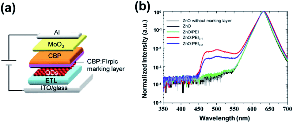 | ||
| Fig. 5 (a) Schematic diagram showing the general structure of the QDLEDs with the CBP:FIrpic luminescent marking layer. (b) EL spectra from these with the various ETLs. A spectrum from a ZnO ETL control device without the marking layer is also included for comparison. | ||
In a previous study, we found that using ZnO:PEI layers leads to an energy level shift of around 0.5 eV,36 similar to that observed upon using neat PEI layer.42 The similar vacuum level shift in the two cases suggests that another factor must be behind the deeper penetration of electrons into the HTL upon using the ZnO:PEI versus ZnO/PEI ETL, and the subsequent significant differences in their stability. We therefore attribute this behavior to differences in charge distribution and in electric fields across the HTL and QD layers, evident from the observations in Fig. 5, S2 and S3.†
To further verify that the use of PEI indeed reduces the supply of electrons, and thereby the conclusion that the deeper penetration of electrons into the HTL in the case of the ZnO:PEI devices must be the result of a higher electric field within the QDLED structure we test the ETLs in unipolar electron-only devices (EOD). The structure of the EOD was similar to the QDLEDs except that the MoO3 layer was replaced by a 10 nm LiF layer. The general device structure of these EODs therefore is: ITO/ETLs/QD/CBP (30 nm)/LiF (10 nm)/Al (100 nm) and is illustrated in Fig. 6(a). Under forward bias, i.e. when ITO is at a more negative potential relative to the Al contact, the injection of holes from the Al contact is blocked by the LiF layer. The flow of current therefore proceeds only by electrons, which get injected in the device at the ITO contact and collected at the Al contact. Fig. 6(b) shows the J–V characteristics of these EODs, each comprising one of the four ETL configurations. As can be seen, the current at any given voltage decreases in the order (from highest to lowest): ZnO → ZnO/PEI → ZnO:PEI0.1 → ZnO:PEI0.3, indicating that electron supply by the ETLs becomes harder in the same direction which is in line with what was inferred from the changes in the J–V characteristics of the QDLEDs in Fig. 1(b). The deeper penetration of electrons into the HTL in the case of the ZnO:PEI ETLs must therefore be the result of a higher internal electric field in these devices, induced by the more difficult supply of electrons. The almost parallel J–V traces and their linearity over the voltage range suggest that electrons can be injected into the CBP HTL from the QD layer and travel across it relatively easily.
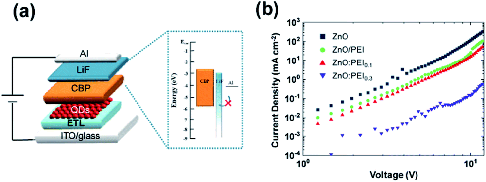 | ||
| Fig. 6 (a) Schematic diagram showing the general structure of the EODs. (b) J–V characteristics of EODs with the different ETLs. | ||
Seeing that the ZnO:PEI ETLs lead to a greater EL stability as well as a deeper penetration of electrons into the HTL, we also carry out comparative delayed EL measurements on QDLEDs with ZnO:PEI0.3, ZnO/PEI and ZnO ETLs to try to glean additional insights into the influence of the various ETLs on altering charge distribution within the devices. The delayed EL measurements are performed using an experimental setup as described in previous work38 and for which a schematic is provided in Fig. S5 of the ESI.† In the delayed EL technique, the QDLEDs are driven with a 500 μs forward bias square pulse of magnitude equivalent to the driving voltage required to achieve a current density of 20 mA cm−2 and allow prompt EL to reach steady state (i.e. 4 V, 5.5 V, and 8 V for the ZnO, ZnO/PEI, and ZnO:PEI0.3 QDLEDs, respectively). Modulating the forward bias voltage to obtain the same current density ensures that the number of charges injected during the forward bias pulse is similar in all devices. It also allows for the study of delayed EL behaviour for devices under the same electrical driving conditions that the EL stability tests were conducted. An optical chopper system is activated to record the EL 50 μs following the end of the forward bias pulse. This delay is sufficiently long for all allowable luminescent exciton relaxation processes to occur and is much larger than a typical QDLED electrical time constant, rendering electrical transient effects negligible. Therefore, any measured EL signal will arise from radiative decay of excitons that are formed after the termination of the forward bias pulse. Fig. 7(a) depicts the delayed EL intensity signal versus time collected from the QDLEDs. In this figure, time = 0 on the x-axis corresponds to 50 μs after the end of the forward bias, the time when the optical chopper is completely open. The data are normalized to the intensity at time = 0 to facilitate comparison. The delayed EL signal has the same decay rate in all devices, suggesting that the mechanistic process behind the delayed EL is the same in all of them. In general, the formation of excitons after the termination of the forward bias pulse in QDLEDs can arise from two processes: (i) recombination of residual (trapped/accumulated) charges in the various device layers including the HTL that become mobile and capable of recombination, producing luminescence after the forward bias pulse has ended and/or (ii) triplet excitons created within the HTL that diffuse slowly and eventually reach and excite the QDs by energy transfer either directly from those triplet states (by a Dexter process) or by a Förster process from singlet intermediates produced by triplet–triplet annihilation (TTA). To identify the main process behind the delayed EL, we investigate the effect of applying a reverse bias pulse, 200 μs long, applied 650 μs after the opening of the optical chopper on the delayed EL characteristics. It is known that in devices where process (i) is the dominant mechanism behind the delayed EL, the application of a reverse bias will lead to a permanent reduction in the delayed EL intensity and is sometimes accompanied by the appearance of EL spikes at the beginning and end of the reverse bias pulse due to the redistribution of charges which provides opportunities for electron–hole recombination.21 On the other hand, in devices where process (ii) is more dominant, the reverse bias will result in only a temporary decrease in the delayed EL signal due to electric-field induced dissociation of excitons which recovers completely after the reverse bias ends. Fig. 7(b–d) show the effect of applying a reverse bias pulse of two different magnitudes (5 V and 7.5 V) on the delayed EL signal from the same set of devices. The data are normalized to the delayed EL intensity at t = 0 in order to facilitate the comparison. As can be seen, in addition to the temporary decrease in EL intensity during the pulse, the reverse bias leads to a permanent reduction in the intensity (observed over the 0.4–0.6 ms range in the figures) as well as a sharp delayed EL spike at the end of the pulse (observed at 0.4 ms in the figures), indicating that the delayed EL arises primarily from the recombination of residual charges (i.e. process (i)). In this regard, the reverse bias sweeps out residual electrons and holes in the device layers towards the cathode and anode respectively, away from the QD EML. Therefore, when the reverse bias ends, some of these charges move back towards each other, driven by diffusion and coulombic forces, producing new electron–hole recombination events and hence the EL spike at the end of the reverse bias. The subsequent permanent reduction in the delayed EL intensity, on the other hand, is due to the permanent removal of residual charges by the reverse bias. As seen, this permanent reduction is larger in the case of the ZnO and ZnO/PEI devices relative to their ZnO:PEI0.3 counterpart (and is larger, although only marginally, in the ZnO device relative to the ZnO/PEI device). The larger reduction suggests that residual charges in these devices are generally more mobile and thus can be swept out more easily by the reverse bias. By contrast, the smaller reduction in the case of the ZnO:PEI0.3 device points to the presence of a significant number of less mobile (i.e. strongly trapped) charges. One can also see that increasing the magnitude of the reverse bias (from 5 V to 7.5 V) does not appreciably affect the magnitude of this reduction in the case of the ZnO/PEI or the ZnO devices, again pointing to the more mobile nature of the residual charges in them which makes it possible for even the lower reverse bias to sweep them out as effectively. This is in contrast to what is observed in the case of the ZnO:PEI0.3 device where the higher reverse voltage leads to a larger reduction in the delayed EL, reflecting the role that the reverse bias plays in detrapping the immobile (i.e. strongly trapped) charges that are present in this case. Although it is not possible to determine the polarity or location of these trapped charges from the delayed EL characteristics, correlating these results with those from the FIrpic marking layer devices (Fig. 5) suggests that they may indeed be electrons in the CBP HTL. This is also in view of the fact that electrons have a much lower mobility compared to holes in CBP (electron mobility and hole mobility are 3 × 10⁻⁴ cm2 V−1 s−1 and 2 × 10⁻³ cm2 V−1 s−1, respectively.43) and hence need higher reverse voltages to be detrapped from their sites in the HTL bulk. This would suggest that some of the electrons that penetrate into the HTL in the case of the ZnO:PEI devices remain deeply trapped in the HTL. This may perhaps explain the different trajectories of the driving voltage versus time trends in Fig. 3(b) where the ETLs that lead to a deeper penetration of electrons into the HTL (i.e. ZnO:PEI0.3 and ZnO:PEI0.1) eventually lead to a faster voltage rise relative to the ZnO/PEI ETL that leads to only limited electron penetration. Because in the case of the ZnO:PEI devices the location of this electron space charge is deep inside the HTL away from the QD interface, it does not appreciably quench the luminescence of the QDs and therefore does not affect the EQE. By contrast, the more mobile charges in the ZnO and ZnO/PEI devices might therefore be holes in the CBP HTL. Regardless of the specific polarity of the charges or their location, the delayed EL results clearly show that the ZnO:PEI0.3 ETL significantly alters charge distribution in the device (much more than the ZnO/PEI ETL) changing the nature of residual charges that remain unrecombined from ones that are more mobile to ones that are more strongly trapped. It is also important to point out that the ZnO/PEI device shows an additional delayed EL spike at the beginning of the forward bias pulse. That only this device shows this spike suggests that residual charges in the PEI layer may be involved in its appearance. (For example, holes that reach the PEI layer and get trapped into it during the forward bias pulse then get detrapped and pulled back towards the QD layer upon applying the reverse bias pulse where they recombine with residual electrons.)
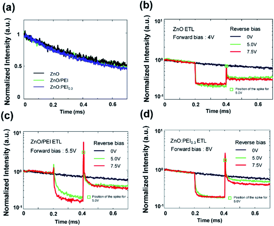 | ||
| Fig. 7 (a) Delayed EL characteristics of the QDLEDs collected after driving with a forward bias square pulse. The magnitude of the driving voltage was adjusted to achieve a current density of 20 mA cm−2 in all cases (i.e. 4 V, 5.5 V, and 8 V for the ZnO, ZnO/PEI, and ZnO:PEI0.3 QDLEDs, respectively). Delayed EL characteristics from the QDLEDs with the ZnO (b), ZnO/PEI (c) and ZnO:PEI0.3 (d) ETLs showing the effect of applying a 200 μs reverse bias pulse with increasing magnitudes on the delayed EL signal. The reverse bias pulse is applied at 0.2 ms. | ||
Conclusions
In conclusion, we investigated the effect of adding PEI to ZnO to form a blended ZnO:PEI ETL instead of using it in a separate layer on the performance of inverted QDLEDs. Results show that the ZnO:PEI blended ETL improves device efficiency by more than 50% compared to the QDLED with only the ZnO ETL. The efficiency improvement is on par with that produced by the ZnO/PEI ETL. More remarkably however, the ZnO:PEI ETL has a significant advantage in terms of improving device stability. A device with a ZnO:PEI ETL containing 0.3 wt% PEI exhibits an LT50 of 153735 hours (for L0 of 100 cd m−2), almost 5× longer than a device with a ZnO/PEI ETL and 10× longer than a ZnO ETL control device. Tests on devices that contain a luminescent marking layer reveal that the ZnO:PEI ETL results in a deeper penetration of electrons into the HTL in comparison to ZnO/PEI or ZnO ETLs, likely due to changes in electric field distribution that also facilitate hole injection from the HTL to the QD and reduce hole accumulation at the QD/HTL interface. Results from electron-only devices and delayed EL measurements show that the ZnO:PEI ETL alters charge distribution in the HTLs changing the nature of residual charges that remain unrecombined in the device from ones that are more mobile to ones that are more strongly trapped, corroborating the conclusion that the stability enhancement is associated with reduced charge accumulation at the QD/HTL interface. The findings show that ZnO:PEI ETLs can be used for enhancing both the efficiency and stability of QDLEDs. They also provide new insights into the importance of managing charge distribution in the charge transport layers for realizing high stability QDLEDs and new approaches to achieve that.
Author contributions
D. S. C. designed and conducted the experiments and D. S. C. and H. A. wrote the paper. All authors contributed to the data analysis and scientific discussion.Conflicts of interest
The authors declare no competing financial interest.Acknowledgements
Partial support to this work by the Natural Sciences & Engineering Research Council of Canada (NSERC) is gratefully acknowledged.References
- V. L. Colvin, M. C. Schlamp and A. P. Alivisatos, Nature, 1994, 370, 354–357 CrossRef CAS.
- D. Bera, L. Qian, T.-K. Tseng and P. H. Holloway, Materials, 2010, 3, 2260–2345 CrossRef CAS.
- Y. Shirasaki, G. J. Supran, M. G. Bawendi and V. Bulović, Nat. Photonics, 2013, 7, 13 CrossRef CAS.
- J. M. Pietryga, Y.-S. Park, J. Lim, A. F. Fidler, W. K. Bae, S. Brovelli and V. I. Klimov, Chem. Rev., 2016, 116, 10513–10622 CrossRef CAS PubMed.
- A. Litvin, I. Martynenko, F. Purcell-Milton, A. Baranov, A. Fedorov and Y. Gun'Ko, J. Mater. Chem. A, 2017, 5, 13252–13275 RSC.
- A. R. Kirmani, J. M. Luther, M. Abolhasani and A. Amassian, ACS Energy Lett., 2020, 5, 3069–3100 CrossRef CAS.
- Y.-S. Park, J. Roh, B. T. Diroll, R. D. Schaller and V. I. Klimov, Nat. Rev. Mater., 2021, 1–20 Search PubMed.
- J. Song, O. Wang, H. Shen, Q. Lin, Z. Li, L. Wang, X. Zhang and L. S. Li, Adv. Funct. Mater., 2019, 29, 1808377 CrossRef.
- D. Liu, S. Cao, S. Wang, H. Wang, W. Dai, B. Zou, J. Zhao and Y. Wang, J. Phys. Chem. Lett., 2020, 11, 3111–3115 CrossRef CAS PubMed.
- J. H. Chang, P. Park, H. Jung, B. G. Jeong, D. Hahm, G. Nagamine, J. Ko, J. Cho, L. A. Padilha and D. C. Lee, ACS Nano, 2018, 12, 10231–10239 CrossRef CAS PubMed.
- S. Chen, W. Cao, T. Liu, S.-W. Tsang, Y. Yang, X. Yan and L. Qian, Nat. Commun., 2019, 10, 1–9 CrossRef PubMed.
- W. Ji, Y. Tian, Q. Zeng, S. Qu, L. Zhang, P. Jing, J. Wang and J. Zhao, ACS Appl. Mater. Interfaces, 2014, 6, 14001–14007 CrossRef CAS PubMed.
- H. Zhang, N. Sui, X. Chi, Y. Wang, Q. Liu, H. Zhang and W. Ji, ACS Appl. Mater. Interfaces, 2016, 8, 31385–31391 CrossRef CAS PubMed.
- H. Moon, C. Lee, W. Lee, J. Kim and H. Chae, Adv. Mater., 2019, 31, 1804294 CrossRef PubMed.
- B. S. Mashford, M. Stevenson, Z. Popovic, C. Hamilton, Z. Zhou, C. Breen, J. Steckel, V. Bulovic, M. Bawendi and S. Coe-Sullivan, Nat. Photonics, 2013, 7, 407–412 CrossRef CAS.
- H. Ishii, K. Sugiyama, E. Ito and K. Seki, Adv. Mater., 1999, 11, 605–625 CrossRef CAS.
- Y.-H. Won, O. Cho, T. Kim, D.-Y. Chung, T. Kim, H. Chung, H. Jang, J. Lee, D. Kim and E. Jang, Nature, 2019, 575, 634–638 CrossRef CAS.
- F. So and D. Kondakov, Adv. Mater., 2010, 22, 3762–3777 CrossRef CAS PubMed.
- T. Davidson-Hall and H. Aziz, Nanoscale, 2019, 11, 8310–8318 RSC.
- H. Yu, Y. Zhang, Y. J. Cho and H. Aziz, ACS Appl. Mater. Interfaces, 2017, 9, 14145–14152 CrossRef CAS PubMed.
- T. Davidson-Hall and H. Aziz, Nanoscale, 2018, 10, 2623–2631 RSC.
- X. Dai, Z. Zhang, Y. Jin, Y. Niu, H. Cao, X. Liang, L. Chen, J. Wang and X. Peng, Nature, 2014, 515, 96–99 CrossRef CAS PubMed.
- D. I. Son, H. H. Kim, S. Cho, D. K. Hwang, J. W. Seo and W. K. Choi, Org. Electron., 2014, 15, 886–892 CrossRef CAS.
- W. Lee, B. Kim, Y. Choi and H. Chae, Opt. Express, 2020, 28, 33971–33981 CrossRef CAS PubMed.
- Q. Lin, L. Wang, Z. Li, H. Shen, L. Guo, Y. Kuang, H. Wang and L. S. Li, ACS Photonics, 2018, 5, 939–946 CrossRef CAS.
- S. Hussain, A. Subramanian, S. Yan, N. Din, G. Abbas, A. Shuja, W. Lei and Q. Khan, ACS Appl. Electron. Mater., 2020, 2, 2383–2389 CrossRef CAS.
- K. Ding, H. Chen, L. Fan, B. Wang, Z. Huang, S. Zhuang, B. Hu and L. Wang, ACS Appl. Mater. Interfaces, 2017, 9, 20231–20238 CrossRef CAS PubMed.
- Q. Yuan, X. Guan, X. Xue, D. Han, H. Zhong, H. Zhang, H. Zhang and W. Ji, Phys. Status Solidi RRL, 2019, 13, 1800575 CrossRef.
- R. Kaçar, S. P. Mucur, F. Yıldız, S. Dabak and E. Tekin, Nanotechnology, 2017, 28, 245204 CrossRef PubMed.
- R. Kaçar, S. P. Mucur, F. Yıldız, S. Dabak and E. Tekin, Appl. Phys. Lett., 2018, 112, 163302 CrossRef.
- S. Stolz, Y. Zhang, U. Lemmer, G. Hernandez-Sosa and H. Aziz, ACS Appl. Mater. Interfaces, 2017, 9, 2776–2785 CrossRef CAS PubMed.
- H.-C. Chen, S.-W. Lin, J.-M. Jiang, Y.-W. Su and K.-H. Wei, ACS Appl. Mater. Interfaces, 2015, 7, 6273–6281 CrossRef CAS PubMed.
- X. Jia, N. Wu, J. Wei, L. Zhang, Q. Luo, Z. Bao, Y.-Q. Li, Y. Yang, X. Liu and C.-Q. Ma, Org. Electron., 2016, 38, 150–157 CrossRef CAS.
- C. Liu, Z. Li, X. Zhang, W. Guo, L. Zhang and S. Ruan, ACS Photonics, 2017, 4, 2952–2958 CrossRef CAS.
- J. Wei, C. Zhang, G. Ji, Y. Han, I. Ismail, H. Li, Q. Luo, J. Yang and C.-Q. Ma, Sol. Energy, 2019, 193, 102–110 CrossRef CAS.
- M. Sadeghianlemraski, B. Y. Lee, T. Davidson-Hall, Z. Leonenko and H. Aziz, Org. Electron., 2019, 73, 26–35 CrossRef CAS.
- Y.-L. Shi, F. Liang, Y. Hu, M.-P. Zhuo, X.-D. Wang and L.-S. Liao, Nanoscale, 2017, 9, 14792–14797 RSC.
- T. Davidson-Hall and H. Aziz, ACS Appl. Mater. Interfaces, 2020, 12, 16782–16791 CrossRef CAS PubMed.
- T. Davidson-Hall and H. Aziz, Appl. Phys. Lett., 2020, 116, 010502 CrossRef CAS.
- J. Lim, Y.-S. Park and V. I. Klimov, Nat. Mater., 2018, 17, 42–49 CrossRef CAS PubMed.
- Z. Zhang, X. Guan, Z. Kang, H. Zhang, Q. Zeng, R. Yu, R. Wang and W. Ji, Org. Electron., 2019, 73, 337–341 CrossRef CAS.
- D. Kim, Y. Fu, S. Kim, W. Lee, K.-H. Lee, H. K. Chung, H.-J. Lee, H. Yang and H. Chae, ACS Nano, 2017, 11, 1982–1990 CrossRef CAS PubMed.
- J.-H. Jou, S. Kumar, M. Singh, Y.-H. Chen, C.-C. Chen and M.-T. Lee, Molecules, 2015, 20, 13005–13030 CrossRef CAS PubMed.
Footnote |
| † Electronic supplementary information (ESI) available: Exciton lifetime of QDs on ZnO:PEI with different concentrations of PEI, driving voltage dependence of the EL spectra of QDLEDs with an FIrpic marking layer, experimental setup for delayed EL. See DOI: 10.1039/d1na00561h |
| This journal is © The Royal Society of Chemistry 2021 |