DOI:
10.1039/D1NA00563D
(Paper)
Nanoscale Adv., 2021,
3, 5908-5918
Tuning the band gap and carrier concentration of titania films grown by spatial atomic layer deposition: a precursor comparison†
Received
20th July 2021
, Accepted 31st August 2021
First published on 31st August 2021
Abstract
Spatial atomic layer deposition retains the advantages of conventional atomic layer deposition: conformal, pinhole-free films and excellent control over thickness. Additionally, it allows higher deposition rates and is well-adapted to depositing metal oxide nanofilms for photovoltaic cells and other devices. This study compares the morphological, electrical and optical properties of titania thin films deposited by spatial atomic layer deposition from titanium isopropoxide (TTIP) and titanium tetrachloride (TiCl4) over the temperature range 100–300 °C, using the oxidant H2O. Amorphous films were deposited at temperatures as low as 100 °C from both precursors: the approach is suitable for applying films to temperature-sensitive devices. An amorphous-to-crystalline transition temperature was observed for both precursors resulting in surface roughening, and agglomerates for TiCl4. Both precursors formed conformal anatase films at 300 °C, with growth rates of 0.233 and 0.153 nm s−1 for TiCl4 and TTIP. A drawback of TiCl4 use is the HCl by-product, which was blamed for agglomeration in the films. Cl contamination was the likely cause of band gap narrowing and higher defect densities compared to TTIP-grown films. The carrier concentration of the nanofilms was found to increase with deposition temperature. The films were tested in hybrid bilayer solar cells to demonstrate their appropriateness for photovoltaic devices.
1. Introduction
Atomic layer deposition (ALD) has a wealth of applications in the electronics industry and in the ever-growing field of nanotechnology.1–4 Continual miniaturisation of devices calls for a deposition method that can produce very thin, high-quality films, and allows for precise control over their growth. Due to the nature of the ALD process, thickness control on the order of angstroms or even monolayers is possible,2 and the conformality on high aspect ratio features is second to none. Atmospheric-pressure spatial atomic layer deposition (AP-SALD) enables a much higher growth rate of nanofilms compared to conventional ALD, while still producing pinhole-free films with atomic-scale thickness control.5–7 While many types of materials can nowadays be deposited by ALD,1 for AP-SALD research has predominantly focused on ZnO8,9 and Al2O3 (ref. 10–15) due to the high vapour pressures of the precursors available for these materials.5 Metal oxides are widely used in photovoltaics and other devices, and the scalable AP-SALD technique is very attractive for their manufacture. In addition to ZnO and Al2O3, AP-SALD has been used to produce TiO2,16,17 Nb2O5,16 Cu2O,18 doped ZnO,19–23 and SnO2 (ref. 24) for photovoltaics. This study focuses on the deposition of TiO2, a wide band gap semiconductor which has a wealth of applications in this field, including for dye-sensitised, organic, colloidal quantum dot, and metal halide perovskite solar cells.
ALD of TiO2 is most commonly carried out using titanium tetrachloride (TiCl4),17,25–33 titanium isopropoxide (Ti(OCH(CH3)2)4, TTIP)34–37 and titanium ethoxide,38,39 with deposition from other precursors such as TiI4 (ref. 40) and tetrakis-dimethylamino-titanium (TDMAT)41 having also been studied. An understanding of the influence of the precursor and deposition conditions used on the properties of the TiO2, including the amorphous-to-crystalline transition, is important when incorporating TiO2 films into devices. TiCl4 is very reactive and can be used over a wide temperature range, having a sufficiently high vapour pressure that additional heating is not required. However, a major disadvantage is the corrosive by-product HCl. Due to its reactivity, HCl may re-adsorb and cause a decrease in growth rate.42 Furthermore, chloride contamination is unfavourable and has also been shown to hinder the crystallisation of films at low temperature.28 The alkoxides (TTIP and titanium ethoxide) do not produce corrosive by-products but can yield lower growth rates than TiCl4,34,38 and suffer from poor thermal stability.1
This study compares the growth of TiO2 by AP-SALD over the temperature range 100–300 °C using two different precursors: TiCl4 and TTIP, and is the first comparison of these precursors for AP-SALD. Even for conventional ALD, to the best of our knowledge, such a comparison of the properties of nanofilms grown from these precursors has not been realised. Film characterisation was carried out by means of X-ray diffraction, UV-vis spectroscopy, and atomic force microscopy. Electrical characterisation and photovoltaic measurements were also conducted to compare the properties of the films made using the two precursors.
2. Experimental
2.1 Film deposition
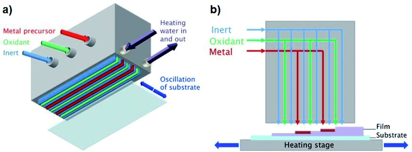
In contrast to conventional ALD, which separates the precursor half-reactions temporally using slow pulsing and purging steps in a vacuum chamber, AP-SALD separates them spatially,4–7,10–12,43 such that the substrate oscillates between regions of different precursors and much higher deposition rates are achieved (e.g. 1 nm s−1vs. 0.03–0.08 nm s−1 for conventional ALD).1,12,13 Here this is achieved with a reactor head containing several gas channels, which supply the metal precursor, oxidant, and inert purging gas to the substrate, as illustrated in Fig. 1(a). In addition to significantly enhanced growth rates, AP-SALD removes the need to operate in a vacuum, as the precursors exit the head at pressures greater than atmospheric pressure,2 making AP-SALD more suitable for high-throughput processing.
 |
| | Fig. 1 (a) Schematic of AP-SALD reactor head with (b) showing sequential layer growth. | |
All films were deposited on borosilicate glass (Soham Scientific, UK, 63.5 × 63.5 × 0.7 mm) or ITO/glass substrates (Präzisions Glas and Optik GmbH, Germany, 14 × 14 × 0.7 mm). A heated substrate stage was used to control the substrate temperature (100–300 °C). For both TiCl4 and TTIP precursors (both from Sigma-Aldrich), water was used as the oxidant, and N2 as the inert purging gas. Nitrogen was bubbled through the Ti precursors and oxidant to generate the reactant vapours, which were combined with additional flows of nitrogen carrier gas. The vapour pressure of TiCl4 at room temperature and atmospheric pressure was sufficient for deposition (1.3 kPa). Due to the lower vapour pressure of TTIP (27 Pa (ref. 44 and 45)), the bubbler was heated to 110 °C to produce sufficient fumes for deposition. The N2 bubbling rates through the precursors and the flow rates through the reactor head channels for both precursors are given in Table S1 of the ESI.† Bubbling rates through the TiCl4 and TTIP were 7 and 100 mL min−1 respectively, the higher rate for the TTIP again owing to its lower volatility. The AP-SALD reactor head contained 2 metal channels and 3 oxidant channels, as shown in Fig. 1(b). Movement of the substrate back and forth underneath the head corresponded to 1 oscillation of 1.8 s, in which time the substrate was exposed to 4 full ALD cycles. Different film thicknesses were achieved by oscillating the substrates for 100–500 oscillations.
2.2 Film characterisation
Film thicknesses were measured using a Dektak profilometer. X-ray diffraction (XRD) measurements were performed using a Bruker D8 theta/theta XRD system with Cu Kα radiation (λ = 0.15418 nm) and a LynxEye position-sensitive detector, scanning from 2θ = 20° to 75°. UV-vis absorbance measurements were performed using an Agilent/HP 8453 UV-vis spectrometer, and the band gap determined from a Tauc plot. Atomic force microscopy (AFM) measurements were performed with a Veeco Multimode Nanoscope III system operating in tapping mode with a scan size of 2 × 2 μm. A LEO VP1530 field emission scanning electron microscope (SEM) was used for energy dispersive X-ray spectroscopy (EDX) measurements. The samples analysed were on glass substrates, and a thin layer of carbon was sputter-coated on the cross-sections to prevent charging of the samples during imaging.
2.3 Electrical characterisation
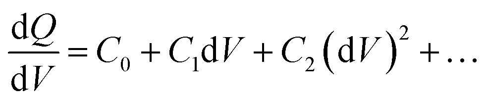
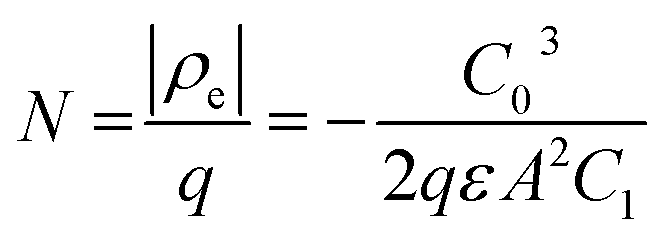
Drive-level capacitance profiling (DLCP) was performed using an Agilent 4294A impedance analyzer. This technique has been used for amorphous silicon films46 and polycrystalline Cu(In,Ga)Se2 films,47 among others. The junction capacitance technique of capacitance–voltage (CV) profiling (whereby the capacitance of a Schottky barrier junction is measured as a function of applied DC bias) can overestimate the carrier density of semiconductor materials that have a large number of defect states within the band gap. This means CV profiling is, in general, inappropriate for measuring the carrier density of amorphous and polycrystalline thin films. In this study, AFM and XRD measurements will show that the films are either amorphous or polycrystalline, thus prompting the use of the DLCP technique to measure the carrier densities. A detailed description of DLCP theory can be found in ref. 47 and 48 but a brief overview is given here. Prior to measurement, TiO2 films on ITO were masked with Kapton tape and aluminium contacts (∼50 nm, 0.225 cm2) were evaporated using an Edwards resistance evaporator. Finally, a small dot of silver paste was applied to make electrical contact between the device contact and the tape where the measurement probe was placed. A Schottky barrier and ohmic contact are expected at the TiO2/ITO and TiO2/Al junctions, respectively. For measurement, the positive terminal of the impedance analyzer was connected to the Al, and the negative one to the ITO. A large AC voltage is applied to the sample such that a non-linear charge response (dQ/dV) is produced (with very small AC voltages, a linear charge response is assumed).| | 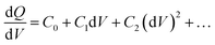 | (1) |
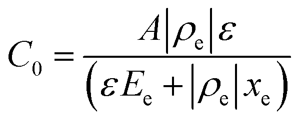
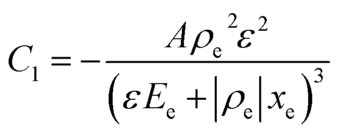
whereby:| | 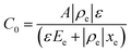 | (2) |
and| |  | (3) |
Here ρe is the charge density, ε is the permittivity of the medium (=κε0), A is the area of the contact and Ee is the electric field magnitude at point xe within the junction. As the AC bias is altered, so is the DC bias, such that the maximum applied voltage, V = VAC + VDC, stays constant and a single location in the junction is probed. A table of the combinations of AC and DC biases that were used to give a maximum voltage of −0.1 V is included in Table S2 of the ESI.† The AC bias is applied to increase the reverse bias imposed by the DC bias, as shown in Fig. S1.† The capacitance was measured for a range of angular frequencies (ω) between 40 Hz and 10 MHz, and for each one a plot of C against AC bias was produced. C0 and C1 can be obtained for each frequency from a second order fit of capacitance, and the corresponding carrier density (N) and position in the junction (xe) calculated from eqn (4) and (5). A spatial profile of the carrier density in the sample can then be formed by plotting N vs. xe.
| | 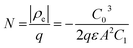 | (4) |
and
| |  | (5) |
Here q is the elementary charge. At large frequencies (high xe), the value of N will approach that of the free carrier density. At low ω (low xe), N is the maximum density of states that can respond to the AC bias: both deep states and shallow donors. Defect densities are thus taken to be the difference between these maximum and minimum values of N.47
2.4 Photovoltaic fabrication and measurements
ITO-coated glass substrates (Präzisions Glas and Optik GmbH, Germany) with TiO2 films deposited at 300 °C from both precursors were sonicated in ethanol, then heated to 120 °C for 10 min. Sepiolid P200 P3HT (poly(3-hexylthiophene-2,5-diyl), Rieke Metals, Inc.) was dissolved in chlorobenzene at a concentration of 15 mg mL−1 and stirred at 40 °C. 125 μL of the polymer was spin-coated onto the titania-coated ITO substrates at 600 rpm for 6 s, then 1000 rpm for 1 min. This was followed by annealing in air for 15 min at 150 °C, before contacts consisting of 80 nm of Ag on top of 7 nm of MoO3 were thermally evaporated using a shadow mask. 8 Contacts (each of 4.5 mm2) were deposited atop each substrate. Current density–voltage measurements were made using a Keithley 2636 SourceMeter under an Oriel 92550A solar simulator (AM1.5G), at an intensity equivalent to 100 mW cm−2 after correcting for spectral mismatch.
3. Results and discussion
3.1 Effect of precursor and deposition temperature on film growth rates
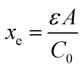
TiO2 thin films were fabricated by AP-SALD at different temperatures using TiCl4 and TTIP. Fig. 2 illustrates the growth rate of TiO2 from TiCl4 and TTIP as a function of deposition temperature. Each data point in Fig. 2 was produced by depositing several films of different thicknesses at a fixed temperature, calculating the growth rate for each sample (thickness/number of oscillations), and then calculating the average growth rate at that temperature. An example data set and calculation of the growth rate is given in Table S3 of the ESI.† The calculation assumes that the growth rate is independent of film thickness. Deviation from such an assumption has been considered34 and will be addressed in Section 3.3.
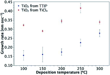 |
| | Fig. 2 Growth rate of TiO2 films from TiCl4 and TTIP as a function of deposition temperature. | |
Overall, there is a distinct difference in the shape of the curves for deposition from each precursor, with maximum observed growth rates of 0.42 nm per oscillation and 0.28 nm per oscillation for TiCl4 and TTIP respectively, corresponding to 0.10 and 0.07 nm per cycle (or 0.233 and 0.153 nm s−1). For films deposited from TiCl4, there is little variation in the growth rate with temperature, apart from the increase observed at 250 °C. As will be discussed in Section 3.3, this is found to be the amorphous-to-crystalline transition temperature of these films, which results in the formation of agglomerates and surface roughening. A slight decrease in the growth rate is observed for the TiCl4 precursor when the growth temperature is increased from 100 to 150 °C. This behaviour is not unusual for ALD processes from chloride and water, with decreasing ligand release from adsorbed chloride molecules at higher temperatures proposed as a reason.26 The surface concentration of absorption sites for TiCl4 molecules depends on the substrate temperature. TiCl4 is more reactive with hydroxyl groups than oxygen bridges, such that the Cl ligands can be released and the adsorbed molecule is then smaller in size.49 The concentration of hydroxyl groups on a TiO2 surface has been found to decrease with temperature.50 A larger number of hydroxyl groups gives rise to a larger number of adsorbed molecules and a higher possible surface concentration of adsorbed molecules in a monolayer.
For deposition from TTIP, the growth rate is approximately constant at temperatures between 100 and 200 °C. Although some support was found in the literature for this being the conventional ALD temperature window using TTIP, other reports indicated that the growth rate increased as the temperature was taken from 100 to 200 °C.34,37,51,52 The sharp increase in growth rate for 250 and 300 °C is attributed to thermal decomposition of the precursor (thus outside of the ALD window),1,2,34 which allows further reactant absorption and hence an increased growth rate.2 The growth rate of TiO2 from TiCl4 is higher than that from TTIP across the temperature range investigated. This is attributed to the bulkier isopropoxide ligand compared to chlorine, and hence a larger effective diameter of the TTIP precursor (0.88 and 0.64 nm for TTIP and TiCl4 respectively).25 Larger ligands temporarily block several adsorption sites and reduce the total amount of Ti adsorbed in each ALD cycle.25,34 It is also possible that for the less volatile TTIP precursor, the concentration of precursor arriving on the surface is lower, which reduced the degree of surface saturation.
3.2 Factors affecting film crystallinity
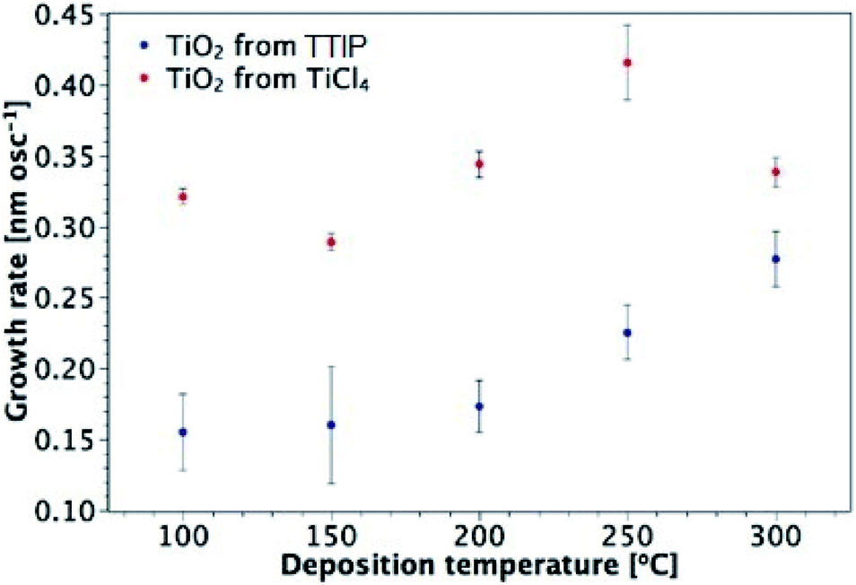
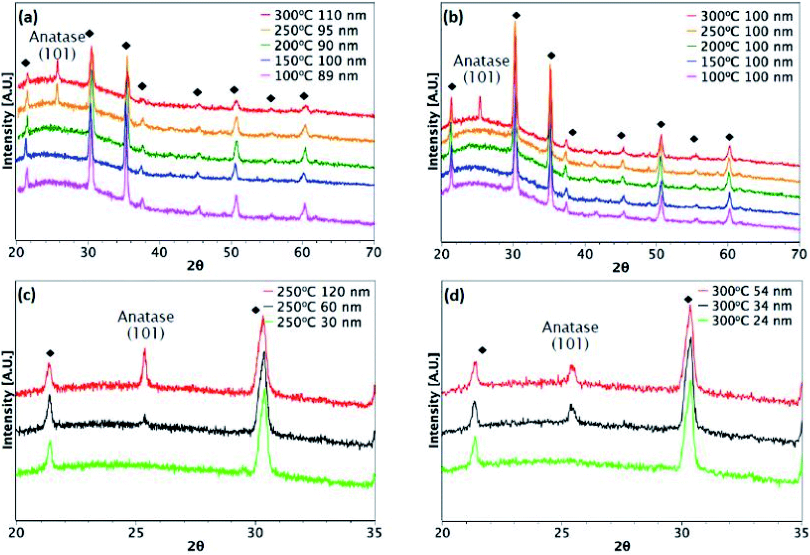
Fig. 3 and 4 show XRD results for TiO2 films grown from both precursors over the temperature range 100–300 °C on glass and ITO/glass substrates, respectively. The temperature at which crystalline anatase starts to form, which is identified by the (101) anatase peak, is dependent on the precursor, film thickness and substrate. Considering first the films deposited on glass, a comparison between Fig. 3(a) and (b) shows that films approximately 100 nm thick undergo crystallisation at 300 °C, regardless of the precursor. However, it is possible to form the anatase phase at 250 °C using TiCl4 when the film thickness is 150 nm and above (Fig. 3(c)). That said, films deposited at 250 °C from TTIP do not undergo crystallisation, even at 180 nm, as shown in Fig. 3(b). At 300 °C, a thickness of 55 nm is required before crystallisation occurs for TTIP (Fig. 3(d)). We propose that the onset of crystallinity for films deposited from TiCl4 is at a lower temperature than films deposited from TTIP due to the smaller size of the TiCl4 ligand. Easier migration of the intermediate surface species would allow for arrangement of the atoms into a crystal structure at a lower temperature.
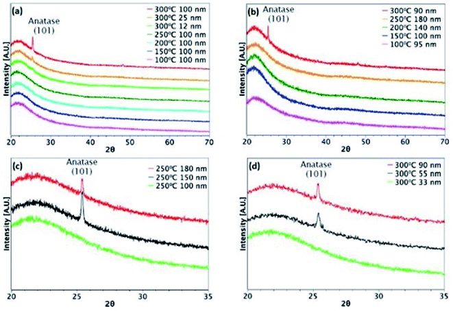 |
| | Fig. 3 XRD patterns for TiO2 films deposited on glass. Films deposited at different temperatures from (a) TiCl4 and (b) TTIP. Different film thicknesses deposited at (c) 250 °C from TiCl4 and (d) 300 °C from TTIP. | |
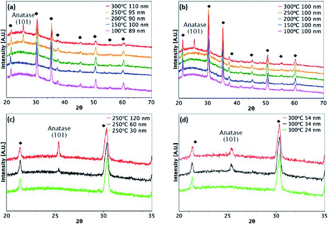 |
| | Fig. 4 XRD patterns for TiO2 films deposited on ITO. Black diamonds indicate peaks from the underlying ITO. Films deposited at different temperatures from (a) TiCl4 and (b) TTIP. Different film thicknesses deposited from (c) TiCl4 at 250 °C and (d) TTIP at 300 °C. | |
The onset of crystallisation is also affected by the substrate. For films deposited from TiCl4, Fig. 3(a) and (c) show that for deposition on glass at 250 °C, the (101)-anatase peak does not appear until a thickness of 150 nm has been attained. On ITO, however (Fig. 4(a) and (c)), crystallisation is observed to occur by 60 nm, suggesting that the underlying crystal structure of the ITO promotes crystallisation. A similar trend is observed for films deposited from TTIP at 300 °C. As with deposition on glass, crystallisation of films deposited from TTIP is not observed to occur until 300 °C (Fig. 4(b)), with crystallisation by thicknesses of 55 nm and 34 nm for glass and ITO substrates, respectively (Fig. 3(d) and 4(d)).
3.3 Factors affecting film morphology and roughness
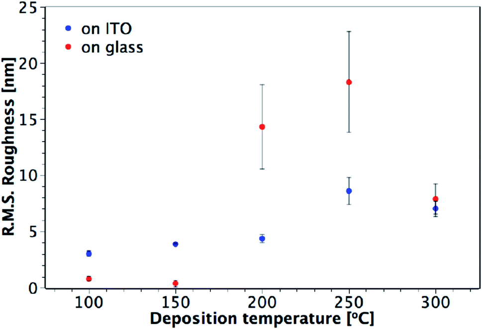
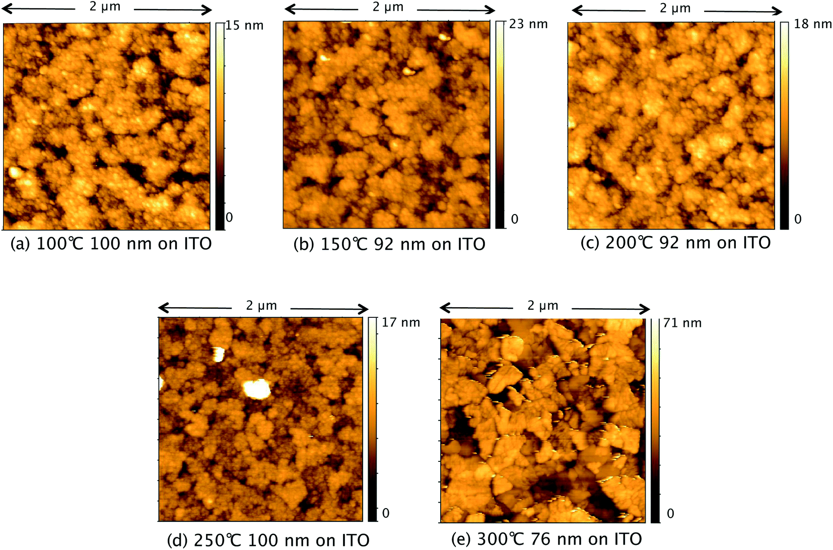
AFM studies revealed that the roughness and morphology of the resulting films were dependent on the deposition temperature and the precursor. Fig. 5 shows images of TiO2 films deposited on ITO from TiCl4 over the temperature range 100–300 °C. Little difference is observed in the morphology and roughness of the films deposited between 100 and 200 °C, with an overall amorphous globular structure that adopts the larger scale morphology of the underlying ITO (substrate shown in Fig. 5(g)). In Fig. 6, a sharp increase in the roughness of the films deposited on ITO using TiCl4 occurs at 250 °C, which is the onset of crystallisation, as previously shown by XRD (Fig. 4). Close inspection of Fig. 5(d) (60 nm sample grown at 250 °C) shows the underlying film to have a similar morphology to those at deposition temperatures of 200 °C and below (i.e. that of the underlying ITO), and that agglomerates have begun to form on top. The formation of these agglomerates coincides with the appearance of the (101) anatase XRD peak, indicating that this is how the anatase first forms in the films. For a thicker TiO2 film deposited at 250 °C (120 nm, Fig. 5(e)), the anatase agglomerates have now covered the entire surface, leaving no trace of the underlying ITO structure. Increasing the deposition temperature further to 300 °C gives rise to sharper, more distinct agglomerates (Fig. 5(f)), with little change in surface roughness (Fig. 6).
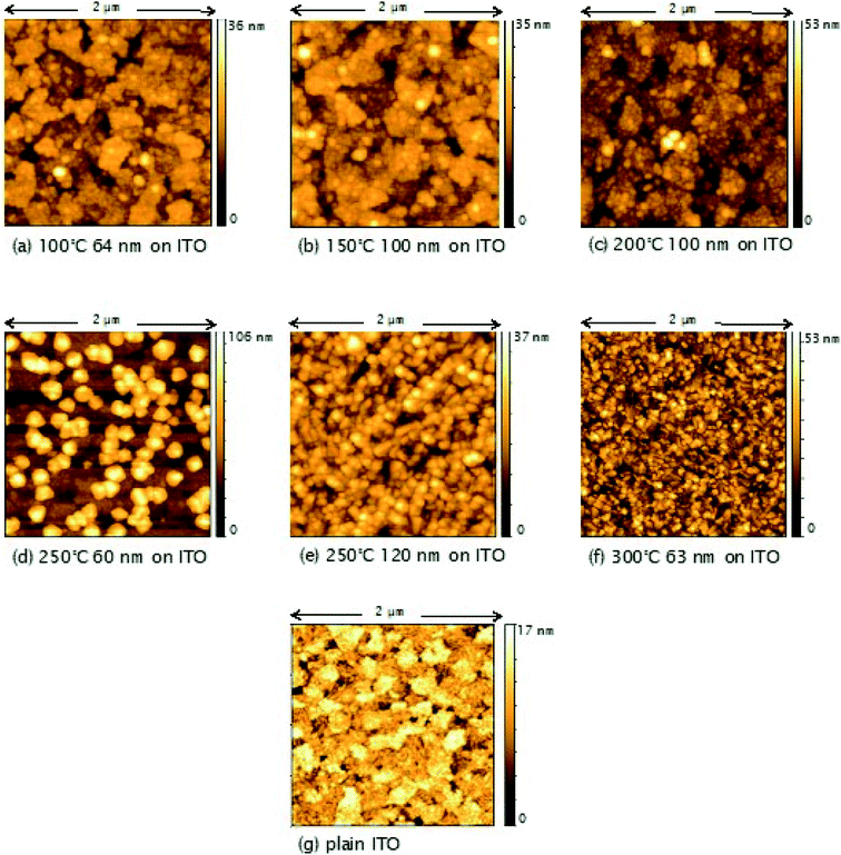 |
| | Fig. 5 AFM images of TiO2 films deposited at different temperatures on ITO from TiCl4. Film thicknesses and deposition temperatures presented under each of the images, labelled (a)–(g). ITO roughness: 2.9 ± 0.3 nm. | |
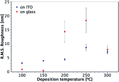 |
| | Fig. 6 Plot showing the variation of R.M.S. roughness with deposition temperature for TiO2 films deposited from TiCl4 on glass and ITO. Film thicknesses are indicated in Fig. 5 and S2.† | |
The high free energy of the film–substrate interface can promote agglomeration to minimise the interface's surface area. Ritala et al. have shown that the presence of HCl vapour (a by-product of the TiCl4 reaction) can accelerate agglomeration.33 Without any migration or gas phase nucleation, the film is expected to grow uniformly over the substrate. However, HCl can produce Ti(OH)2Cl2, a volatile species which provides an effective mechanism for material transportation. The transportation can occur via the intermediate surface species (–O–)nTiCl4−n and (–O–)nTi(OH)4−n as well as via ligand exchange of TiCl4 (eqn (6)). The re-adsorption of the Ti(OH)2Cl2 can then cause agglomeration.
| | | 2(–OH)(s) + TiCl4(g) → 2(–Cl)(s) + Ti(OH)2Cl2(g) | (6) |
Different trends in both morphology and roughness are seen when the films are deposited from TiCl4 on glass (Fig. 6 and S2†). The sharp increase in roughness from 150 to 200 °C seen in Fig. 6 is due to the presence of agglomerates (Fig. S2(c)†), however in this instance they are not crystalline, as these films were found to be amorphous when measured by XRD (Fig. 3). It may be that more controlled film deposition occurs when the films are deposited on crystalline ITO, such that the effect of agglomeration due to the Ti(OH)2Cl2 volatile species is not as pronounced until higher temperatures of 250 °C and above. A ‘globular’ structure can be seen for films deposited at 200 °C on ITO (Fig. 5(c)), but the film still maintains the underlying structure of the ITO, suggesting that interaction with the ITO causes the depositing film to adopt the same structure. On the other hand, when the films are deposited on glass at 200 °C (Fig. S2(c)†), less interaction with the substrate makes it easier for large amorphous agglomerates to form at a lower temperature.
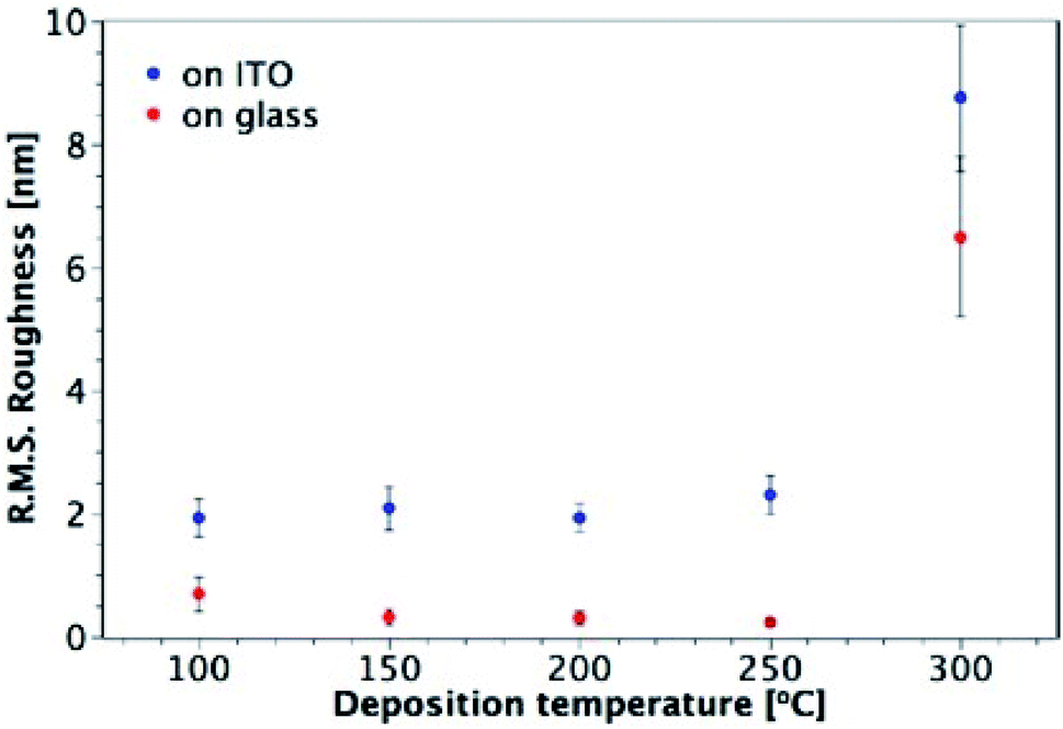
Fig. 7 shows AFM images of TiO2 films deposited from TTIP on ITO, with their corresponding roughness presented in Fig. 8. As for the films made from TiCl4, a sharp increase in roughness was observed at the amorphous-to-crystalline phase transition (300 °C for TTIP). The films deposited on ITO below 300 °C have an amorphous globular structure that takes on the larger-scale morphology of the underlying ITO and the film roughness is similar to that of the ITO (2.9 ± 0.3 nm). At 300 °C the film morphology still resembles that of the ITO, except that the smaller-scale globular structure is no longer present, as the film has transformed to crystalline anatase. Retention of the underlying ITO morphology after the amorphous-to-crystalline phase transition has taken place contrasts with the films made from TiCl4. The absence of HCl as a by-product in this reaction means the volatile species Ti(OH)2Cl2, which can lead to agglomeration, is not produced. AFM images for films deposited from TTIP on glass are presented in Fig. S3.† These films follow the same trend in roughness as their ITO counterparts, as shown in Fig. 8, but have a consistently lower roughness, owing to the smoother surface of the glass. These films do not show the same increase in roughness from 150 to 200 °C as those deposited from TiCl4, which is again attributed to the lack of HCl by-product. As for the depositions on ITO, there is a sharp increase in film roughness at the crystallisation temperature (300 °C), and distinct crystallites 200–400 nm in size can be observed in Fig. S3(e).†
 |
| | Fig. 7 AFM images of TiO2 films deposited at different temperatures on ITO from TTIP. Film thicknesses and deposition temperatures presented under each of the images, labelled (a)–(e). | |
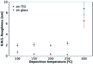 |
| | Fig. 8 Plot showing the variation of R.M.S. roughness with deposition temperature for TiO2 films deposited from TTIP on glass and ITO. Film thicknesses are indicated in Fig. 7 and S3.† | |
The highest surface roughness for films made from the two precursors was observed at the temperature of the amorphous-to-crystalline phase transition: 250 °C for films deposited from TiCl4 and 300 °C for films from TTIP. Such a trend in surface roughness is not unusual for TiO2 films grown by ALD, and has been observed for deposition from both TiCl4 and Ti-ethoxide.28,39 It has been shown that there is a fine balance between the deposition temperature, film morphology and film thickness, and their effect on the growth rate.39 At the amorphous-to-crystalline phase transition temperature, crystalline anatase starts to appear in films of a certain thickness. The onset of crystallinity and the corresponding increase in surface roughness gives rise to a larger surface area and hence to an increase in the growth rate. Such a trend can be seen in Fig. S4† for depositions using TiCl4, where a relatively consistent growth rate was seen for all temperatures except 250 °C, which is where the onset of crystallisation and the formation of agglomerates was observed (between 60 and 120 nm of film thickness).
3.4 Effects on optical properties
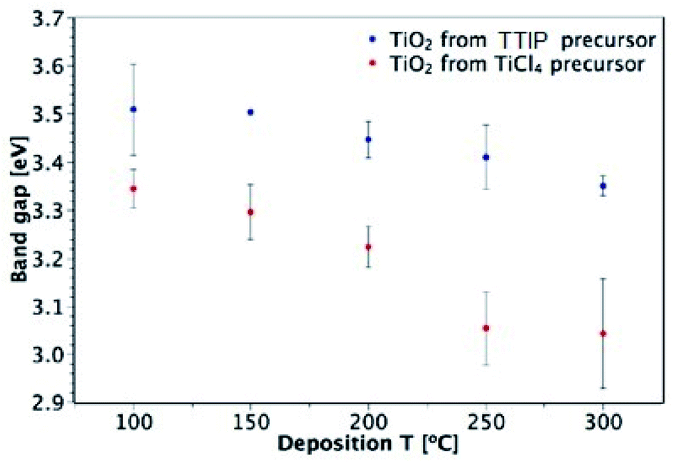
The band gaps of films deposited on glass were determined from UV-vis spectroscopy by plotting a Tauc plot, assuming an indirect transition (see ESI Fig. S5†).53Fig. 9 shows the dependence of the optical band gap on the precursor and deposition temperature for films in the 50–150 nm thickness range. Both precursors produce films that show an overall decrease in band gap with deposition temperature and the films deposited from TiCl4 have consistently lower band gaps than those deposited from TTIP. These results agree with the values reported in literature, as shown in Table 1. As mentioned previously, a downside of using TiCl4 is the potential for chlorine contamination in films. EDX measurements of TiO2 films on glass that were deposited from TiCl4 found chlorine to be present in those deposited at 200 °C and below (Table 2). As the deposition temperature increased from 100 to 200 °C, the Cl![[thin space (1/6-em)]](https://www.rsc.org/images/entities/char_2009.gif) :Ti ratio decreased, with no Cl detectable at 250 and 300 °C. A similar trend was also observed by Aarik et al.27 It may still be the case that a small amount of Cl is present in films at 250 and 300 °C, but it would be below the EDX detection limit (∼1000 ppm). Doping of TiO2 with Cl has previously been shown to shift the absorption edge towards lower energies and thus cause narrowing of the band gap.54 The presence of Cl in the films deposited from TiCl4 is therefore a likely cause of the smaller band gaps observed relative to the films deposited from TTIP.
:Ti ratio decreased, with no Cl detectable at 250 and 300 °C. A similar trend was also observed by Aarik et al.27 It may still be the case that a small amount of Cl is present in films at 250 and 300 °C, but it would be below the EDX detection limit (∼1000 ppm). Doping of TiO2 with Cl has previously been shown to shift the absorption edge towards lower energies and thus cause narrowing of the band gap.54 The presence of Cl in the films deposited from TiCl4 is therefore a likely cause of the smaller band gaps observed relative to the films deposited from TTIP.
 |
| | Fig. 9 Dependence of TiO2 band gap on precursor and deposition temperature (for 50–150 nm-thick films deposited on glass). | |
Table 1 TiO2 band gap values as reported in literature
| Precursor |
Phase |
Band gap [eV] |
Deposition T [°C] |
Deposition method |
Ref. |
| TTIP |
Amorphous |
3.42 |
Room T |
AP-CVD |
55
|
| Anatase |
3.37 |
500 |
AP-CVD |
56
|
| TiCl4 |
Amorphous |
3.33 |
100 |
ALD |
27
|
| Amorphous |
3.36 |
150 |
AP-CVD |
57
|
| Anatase |
3.26 |
300 |
ALD |
27
|
Table 2 EDX measurements of atomic ratio of Cl:Ti in TiO2 films deposited from TiCl4 at different temperatures
| Deposition T [°C] |
Cl:Ti |
| 100 |
0.19 |
| 150 |
0.11 |
| 200 |
0.03 |
| 250 |
0 |
| 300 |
0 |
3.5 Electronic properties
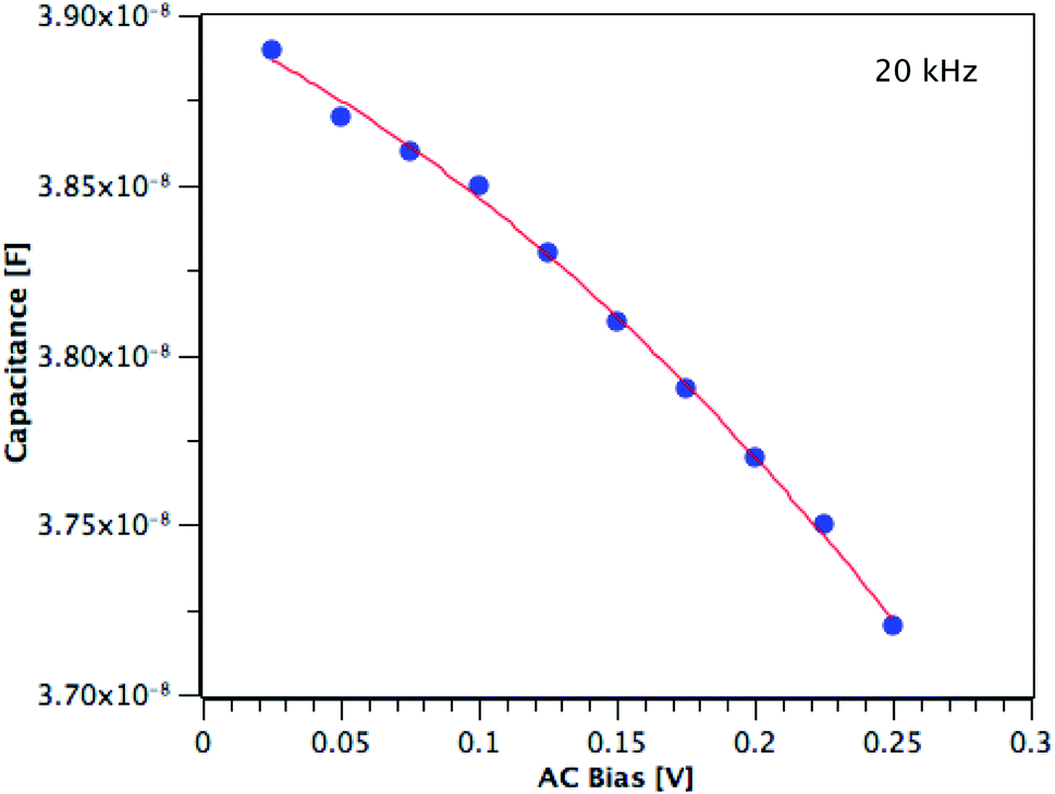
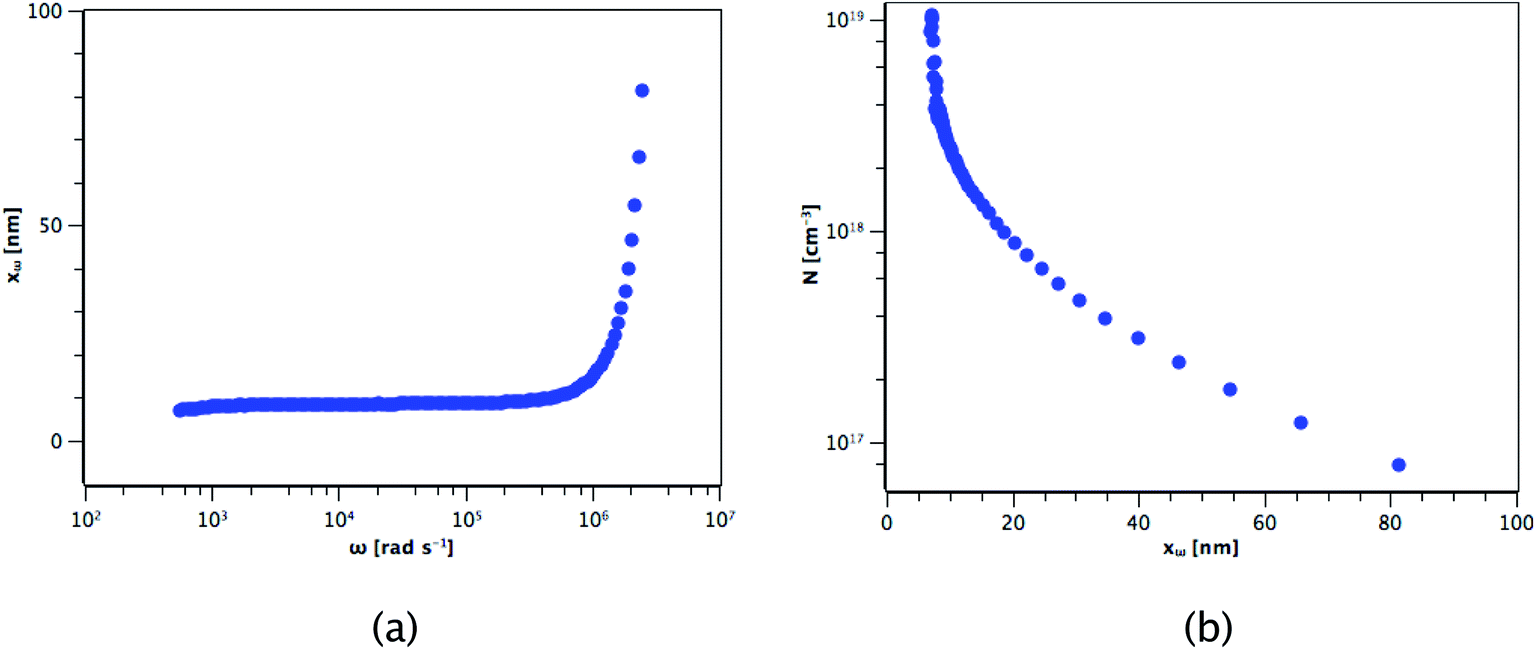
The carrier concentration of the TiO2 films on ITO was measured using DLCP. Fig. 10 shows a plot of C against AC bias for a film deposited from TTIP at 200 °C. Each data point was taken at 20 kHz and a second order fit applied. This process was repeated for 200 frequencies between 40 Hz and 10 MHz, with the resulting xevs. ω and N vs. xe plots given in Fig. 11. It is seen that higher frequencies correspond to larger distances from the TiO2/ITO Schottky junction (xe). At high frequencies (ω), the series resistance of the sample falsely increases the position xe to greater than the sample thickness.48 The TiO2 film thicknesses for the DLCP measurements were ∼50 nm. The profile given in Fig. 11(b) indicates a large carrier concentration in the vicinity of the Schottky junction, which decays as the measurement position moves further into the bulk. A larger N value would be expected at such a location, due to the increased density of trap states. Similarly, N values from the ‘bulk’ of the sample will be a more accurate representation of the free carrier density. As the states in the vicinity of the junction are probed by low frequency measurements, almost all the states present here can respond to the AC bias, and thus the corresponding N value (∼1019 cm−3) represents the maximum density of states present in the sample. The free carrier density (∼1017 cm−3) is that measured in the bulk at high frequencies.
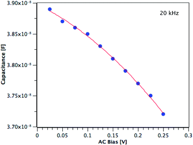 |
| | Fig. 10 Capacitance vs. AC bias at 20 kHz for a TiO2 film deposited from TTIP at 200 °C. | |
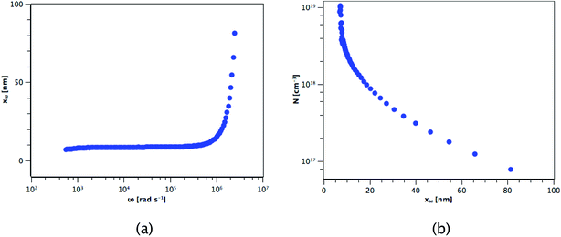 |
| | Fig. 11 Resulting (a) xevs. ω and (b) N vs. xe plots for the film deposited from TTIP. | |
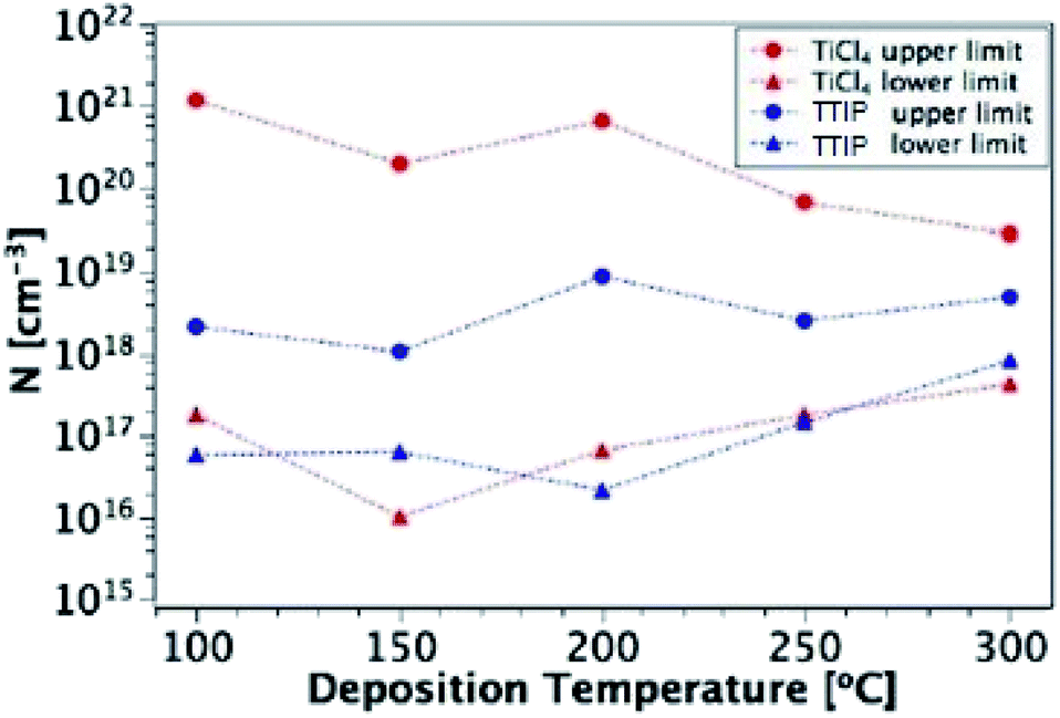
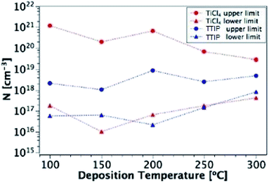
Fig. 12 shows these upper and lower limits of N (maximum and free carrier densities, respectively) for the TiO2 films deposited at different temperatures (100–300 °C) from both precursors. When calculating N, relative permittivity (κ) values of 15 and 35 were used for amorphous and polycrystalline anatase samples respectively, as reported in literature.58–62 The dielectric constant of TiO2 varies little in the range of frequencies presented in Fig. 11 at room temperature, thus the results shown are not expected to be affected by variations in the dielectric constant.63 For both precursors, the free carrier densities show an overall increase in magnitude with deposition temperature, with no major difference between precursors. Where a prominent difference is observed, however, is between the maximum N values produced by each precursor, as shown by the two uppermost lines on the plot. For some deposition temperatures, the values of maximum N for films grown from TiCl4 are almost 3 orders of magnitude higher than the equivalent film made from TTIP. As the difference between the maximum and minimum N values is related to the defect density, this suggests that films made from TiCl4 contain a significantly higher concentration of defects than those made from TTIP. The reason for such a high defect concentration is again likely to be due to the presence of chlorine in the films. The upper limit of the defect concentration for TiCl4 films shows an overall decrease with deposition temperature, as does the Cl content of the films (Table 2).
 |
| | Fig. 12 Upper and lower limits of N for films deposited from TiCl4 and TTIP over the temperature range 100–300 °C. | |
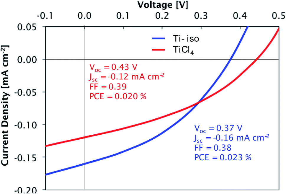
Preliminary tests confirmed the suitability of these films for photovoltaic devices. Films deposited at 300 °C from both precursors were tested in a simple bilayer hybrid solar cell (glass/ITO/TiO2/P3HT/MoO3/Ag). The titania layers were introduced into the solar cells as electron transport layers, responsible for the extraction of electrons from the organic absorber layer P3HT while blocking the entry of holes. The titania layers are sufficiently thin (∼90 nm) to allow efficient transport of electrons to the ITO electrode. The current density–voltage measurements for cells containing each type of film are presented in Fig. 13. A high short-circuit current density (Jsc) and power conversion efficiency (PCE) are not expected for these devices, due to the thin light-absorbing P3HT layer used; however, the devices display a clear photovoltaic effect, demonstrating that suitably compact and smooth films are deposited from each precursor. The slightly larger current density observed in the device with a film made from TTIP is consistent with these films having a lower density of traps as shown by DLCP.
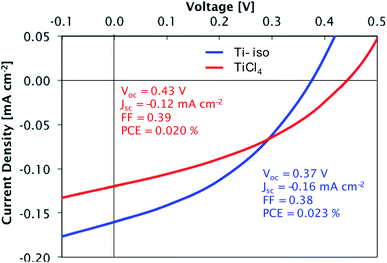 |
| | Fig. 13 Current density–voltage curves for glass/ITO/TiO2/P3HT/MoO3/Ag cells under simulated AM1.5 solar illumination (100 mW cm−2). TiO2 films deposited from TiCl4 and TTIP. | |
4. Conclusions
TiO2 thin films were deposited by AP-SALD while evaluating two precursors, TiCl4 and TTIP, over the temperature range 100–300 °C. Film growth occurred for both precursors over the entire temperature range, with the crystallinity and morphology of the films heavily influenced by the temperature, precursor, substrate, and film thickness. Both precursors formed smooth, conformal anatase films at 300 °C, with growth rates of 0.233 and 0.153 nm s−1 for TiCl4 and TTIP respectively. Conventional ALD growth rates for these precursors range from ∼0.003–0.03 nm s−1, depending on the cycle length and pumping time.26,28,33,34 Deposition from TiCl4 is found to give higher growth rates across the temperature range, which is attributed to the smaller size of the molecule's ligands. The TiCl4 precursor also had the capability to form anatase as low as 250 °C for film thicknesses of 60 nm and above. Conformal amorphous films could also be deposited from both precursors at temperatures as low as 100 °C, making this technique suitable for coating complex structures in temperature-sensitive devices. HCl is an expected by-product of TiO2 film formation from TiCl4 and was found to cause agglomeration in the films. Furthermore, Cl contamination detected in these films led to a ∼0.2 eV narrowing of the band gap compared to those deposited from TTIP. DLCP found the free carrier concentration of the films to be ∼1017 cm−3 for both precursors, with a general increase observed with increasing deposition temperature. The choice of precursor affected the defect density, with films deposited from TiCl4 having a higher one (∼1019 to 1021 cm−3) than those deposited from TTIP (∼1018 cm−3), which was again attributed to the Cl contamination. Incorporating the films into hybrid bilayer solar cells illustrated their suitability as an electron transport layer for photovoltaic devices.
Conflicts of interest
There are no conflicts to declare.
Acknowledgements
K. P. M. acknowledges Girton College (Cambridge) and the Ontario Ministry of Economic Development, Job Creation and Trade (ER18-14-263). C. L. A. acknowledges the Sims Scholarship from the University of Cambridge. J. L. M. D. acknowledges support from the Royal Academy of Engineering Chair in Emerging Technologies scheme (No.: CIET1819_24) and from the European Research Council (ERC) under the European Union's Horizon 2020 research and innovation programme (grant agreement no. 882929 EROS). A. K. acknowledges support from the David and Claudia Harding Foundation. DMR acknowledges Marie Curie Actions (FP7/2007-2013, Grant Agreement No. 219332), the Ramon y Cajal 2011 programme from the Spanish MICINN and the European Social Fund, and the Comissionat per a Universitats I Recerca (CUR) del DIUE de la Generalitat de Catalunya, Spain.
References
- R. W. Johnson, A. Hultqvist and S. F. Bent, Mater. Today, 2014, 17, 236–246 CrossRef CAS.
- S. M. George, Chem. Rev., 2010, 110, 111–131 CrossRef CAS PubMed.
- M. Leskelä and M. Ritala, Thin Solid Films, 2002, 409, 138–146 CrossRef.
- R. L. Z. Hoye, D. Muñoz-Rojas, S. F. Nelson, A. Illiberi, P. Poodt, F. Roozeboom and J. L. MacManus-Driscoll, APL Mater., 2015, 3, 040701 CrossRef.
- P. Poodt, D. C. Cameron, E. Dickey, S. M. George, V. Kuznetsov, G. N. Parsons, F. Roozeboom, G. Sundaram and A. Vermeer, J. Vac. Sci. Technol., A, 2012, 30, 010802 CrossRef.
- K. P. Musselman, C. F. Uzoma and M. S. Miller, Chem. Mater., 2016, 28, 8443–8452 CrossRef CAS.
- D. Munoz-Rojas, T. Maindron, A. Esteve, F. Piallat, J. C. S. Kools and J.-M. Decams, Mater. Today Chem., 2019, 12, 96–120 CrossRef CAS.
- A. Illiberi, F. Grob, C. Frijters, P. Poodt, R. Ramachandra, H. Winands, M. Simor and P. J. Bolt, Prog. Photovoltaics Res. Appl., 2013, 21, 1559–1566 CrossRef CAS.
- D. H. Levy, S. F. Nelson and D. Freeman, J. Disp. Technol., 2009, 5, 484–494 CAS.
- P. Poodt, A. Lankhorst, F. Roozeboom, K. Spee, D. Maas and A. Vermeer, Adv. Mater., 2010, 22, 3564–3567 CrossRef CAS PubMed.
- P. S. Maydannik, T. O. Kääriäinen, K. Lahtinen, D. C. Cameron, M. Söderlund, P. Soininen, P. Johansson, J. Kuusipalo, L. Moro and X. Zeng, J. Vac. Sci. Technol., A, 2014, 32, 051603 CrossRef.
- P. Poodt, R. Knaapen, A. Illiberi, F. Roozeboom and A. van Asten, J. Vac. Sci. Technol., A, 2012, 30, 01A142 CrossRef.
- P. Poodt, V. Tiba, F. Werner, J. Schmidt, a. Vermeer and F. Roozeboom, J. Electrochem. Soc., 2011, 158, H937 CrossRef CAS.
- B. Wegler, O. Schmidt and B. Hensel, J. Vac. Sci. Technol., A, 2015, 33, 01A147 CrossRef.
- P. Poodt, A. Illiberi and F. Roozeboom, Thin Solid Films, 2013, 532, 22–25 CrossRef CAS.
- C. L. Armstrong, M. B. Price, D. Muñoz-Rojas, N. J. K. L. Davis, M. Abdi-Jalebi, R. H. Friend, N. C. Greenham, J. L. MacManus-Driscoll, M. L. Böhm and K. P. Musselman, ACS Nano, 2015, 9, 11863–11871 CrossRef CAS PubMed.
- D. Muñoz-Rojas, H. Sun, D. C. Iza, J. Weickert, L. Chen, H. Wang, L. Schmidt-Mende and J. L. MacManus-Driscoll, Prog. Photovoltaics Res. Appl., 2013, 21, 393–400 CrossRef.
- D. Muñoz-Rojas, M. Jordan, C. Yeoh, A. T. Marin, A. Kursumovic, L. A. Dunlop, D. C. Iza, A. Chen, H. Wang and J. L. MacManus Driscoll, AIP Adv., 2012, 2, 0–7 Search PubMed.
- K. P. Musselman, S. Albert-Seifried, R. L. Z. Hoye, A. Sadhanala, D. Muñoz-Rojas, J. L. MacManus-Driscoll and R. H. Friend, Adv. Funct. Mater., 2014, 24, 3562–3570 CrossRef CAS PubMed.
- B. Ehrler, K. P. Musselman, M. L. Böhm, F. S. F. Morgenstern, Y. Vaynzof, B. J. Walker, J. L. MacManus-Driscoll and N. C. Greenham, ACS Nano, 2013, 7, 4210–4220 CrossRef CAS PubMed.
- Y. Ievskaya, R. L. Z. Hoye, A. Sadhanala, K. P. Musselman and J. L. MacManus-Driscoll, Sol. Energy Mater. Sol. Cells, 2015, 135, 43–48 CrossRef CAS.
- R. L. Z. Hoye, D. Muñoz-Rojas, K. P. Musselman, Y. Vaynzof and J. L. MacManus-Driscoll, ACS Appl. Mater. Interfaces, 2015, 7, 10684–10694 CrossRef CAS PubMed.
- R. L. Z. Hoye, B. Ehrler, M. L. Böhm, D. Muñoz-Rojas, R. M. Altamimi, A. Y. Alyamani, Y. Vaynzof, A. Sadhanala, G. Ercolano and N. C. Greenham, Adv. Energy Mater., 2014, 4, 1301544 CrossRef PubMed.
- L. Hoffmann, K. O. Brinkmann, J. Malerczyk, D. Rogalla, T. Becker, D. Theirich, I. Shutsko, P. Gorrn and T. Riedl, ACS Appl. Mater. Interfaces, 2018, 10, 6006–6013 CrossRef CAS PubMed.
- J. Aarik, A. Aidla, H. Maendar and T. Uustare, Appl. Surf. Sci., 2001, 172, 148–158 CrossRef CAS.
- J. Aarik, A. Aidla, H. Mandar and V. Sammelselg, J. Cryst. Growth, 2000, 220, 531–537 CrossRef CAS.
- J. Aarik, A. Aidla, A. Kiisler, T. Uustare and V. Sammelselg, Thin Solid Films, 1997, 305, 270–273 CrossRef CAS.
- J. Aarik, A. Aidla, T. Uustare and V. Sammelselg, J. Cryst. Growth, 1995, 148, 268–275 CrossRef CAS.
- V. Pore, M. Heikkilä, M. Ritala, M. Leskelä and S. Areva, J. Photochem. Photobiol., A, 2006, 177, 68–75 CrossRef CAS.
- J. S. King, E. Graugnard and C. Summers, J. Adv. Mater., 2005, 17, 1010–1013 CrossRef CAS.
- J. D. Ferguson, A. R. Yoder, A. W. Weimer and S. M. George, Appl. Surf. Sci., 2004, 226, 393–404 CrossRef CAS.
- M. Cameron, I. Gartland, J. Smith and S. Diaz, Langmuir, 2000, 16, 7435–7444 CrossRef CAS.
- M. Ritala, M. Leskela, L.-S. Johansson and L. Niinisto, Thin Solid Films, 1993, 228, 32–35 CrossRef CAS.
- J. Aarik, A. Aidla, T. Uustare, M. Ritala and M. Leskelä, Appl. Surf. Sci., 2000, 161, 385–395 CrossRef CAS.
- M. Ritala, M. Leskela, L. Niinisto, P. Haussalo and L. Niinist, Chem. Mater., 1993, 5, 1174–1181 CrossRef CAS.
- E. R. Cleveland, L. Henn-Lecordier and G. W. Rubloff, J. Vac. Sci. Technol., A, 2012, 30, 01A150 CrossRef.
- Q. Xie, Y.-L. Jiang, C. Detavernier, D. Deduytsche, R. L. Van Meirhaeghe, G.-P. Ru, B.-Z. Li and X.-P. Qu, J. Appl. Phys., 2007, 102, 083521 CrossRef.
- J. Aarik, A. Aidla, V. Sammelselg, T. Uustare, M. Ritala and M. Leskelä, Thin Solid Films, 2000, 370, 163–172 CrossRef CAS.
- J. Aarik, J. Karlis, H. Mändar, T. Uustare and V. Sammelselg, Appl. Surf. Sci., 2001, 181, 339–348 CrossRef CAS.
- J. Aarik, A. Aidla, T. Uustare, K. Kukli, V. Sammelselg, M. Ritala and M. Leskelä, Appl. Surf. Sci., 2002, 193, 277–286 CrossRef CAS.
- M. Reiners, K. Xu, N. Aslam, A. Devi, R. Waser and S. Hoffmann-Eifert, Chem. Mater., 2013, 25, 2934–2943 CrossRef CAS.
- H. Siimon and J. Aarik, J. Phys. D: Appl. Phys., 1997, 30, 1725 CrossRef CAS.
- D. Munoz-Rojas and J. L. MacManus-Driscoll, Mater. Horiz., 2014, 1, 314–320 RSC.
- E. S. Filatov, H. Nizard, P. P. Semyannikov, S. V. Sysoev, S. V. Trubin, N. B. Morozova, K. V. Zherikova and N. V. Gelfond, ECS Trans., 2009, 25, 557–560 CrossRef CAS.
- K. L. Siefering, J. Electrochem. Soc., 1990, 137, 1206–1208 CrossRef CAS.
- T. Unold and J. D. Cohen, Appl. Phys. Lett., 1991, 58, 723 CrossRef CAS.
- J. T. Heath, J. D. Cohen and W. N. Shafarman, J. Appl. Phys., 2004, 95, 1000–1010 CrossRef CAS.
-
A. T. Marin, PhD. thesis, University of Cambridge, 2013.
- J. Aarik, A. Aidla, A.-A. Kiisler, T. Uustare and V. Sammelselg, Thin Solid Films, 1999, 340, 110–116 CrossRef CAS.
- S. Bourgeois, F. Jomard and M. Perdereau, Surf. Sci., 1992, 279, 349–354 CrossRef CAS.
- M. Reinke, Y. Kuzminykh and P. Hoffmann, J. Phys. Chem. C, 2016, 120, 4337–4344 CrossRef CAS.
- M.-H. Jang and Y. Lei, J. Vac. Sci. Technol., A, 2020, 38, 062405 CrossRef CAS.
- G. K. Mor, O. K. Varghese, M. Paulose and C. A. Grimes, Adv. Funct. Mater., 2005, 15, 1291–1296 CrossRef CAS.
- H. Luo, T. Takata, Y. Lee, J. Zhao, K. Domen and Y. Yan, Chem. Mater., 2004, 16, 846–849 CrossRef CAS.
- Z. Sun, X. Li, X. Zhu, X. Deng, D. Chang and A. Zhu, Chem. Vap. Deposition, 2014, 20, 8–13 CrossRef CAS.
- C. S. Chua, X. Fang, X. Chen, O. K. Tan, M. S. Tse, A. M. Soutar and X. Ding, Chem. Vap. Deposition, 2014, 20, 44–50 CrossRef CAS.
- L. Di, C. Shi, X. Li, J. Liu and A. Zhu, Chem. Vap. Deposition, 2012, 18, 309–314 CrossRef CAS.
-
Q. Cheng, W. Ahmad, G. Liu and K. Wang, 2011 11th IEEE International Conference on Nanotechnology, 2011, pp. 1598–1601 Search PubMed.
- M. Stamate, G. Lazar and I. Lazar, Rom. J. Phys., 2008, 53, 217–221 CAS.
- W. Lee, S. Woo, J. Kim, S. Choi and K. Oh, Thin Solid Films, 1994, 237, 105–111 CrossRef CAS.
- H. Tang, K. Prasad, R. Sanjinees, P. E. Schmid and F. Levy, J. Appl. Phys., 1994, 75, 2042 CrossRef CAS.
- S. Kim, W. Kim, K. Kim, C. Hwang and J. Jeong, Appl. Phys. Lett., 2004, 85, 4112 CrossRef CAS.
- K. P. Priyanka, S. Joseph, S. Thankachan, E. M. Mohammed and T. Varghese, J. Basic Appl. Phys., 2013, 2, 105–108 Search PubMed.
Footnote |
| † Electronic supplementary information (ESI) available. See DOI: 10.1039/d1na00563d |
|
| This journal is © The Royal Society of Chemistry 2021 |
Click here to see how this site uses Cookies. View our privacy policy here. 
 Open Access Article
 This Open Access Article is licensed under a Creative Commons Attribution-Non Commercial 3.0 Unported Licence
 bc,
David
Muñoz-Rojas
bc,
David
Muñoz-Rojas