DOI:
10.1039/D1NA00154J
(Paper)
Nanoscale Adv., 2021,
3, 2837-2845
MoS2 and Janus (MoSSe) based 2D van der Waals heterostructures: emerging direct Z-scheme photocatalysts†
Received
28th February 2021
, Accepted 17th March 2021
First published on 18th March 2021
Abstract
Two-dimensional (2D) materials, viz. transition metal dichalcogenides (TMD) and transition metal oxides (TMO), offer a platform that allows the creation of heterostructures with a variety of properties. The optoelectronic industry has observed an upheaval in the research arena of MoS2 based van der Waals (vdW) heterostructures (HTSs) and Janus structures. Therefore, interest towards these structures is backed by the ability to select their electronic and optical properties. The present study investigates the photocatalytic abilites of bilayer, MoS2 and Janus (MoSSe) based vdW HTSs, viz. MoS2/TMO, MoS2/TMD, MoSSe/TMO and MoSSe/TMD, by a first-principles based approach under the framework of (hybrid) density functional theory (DFT) and many body perturbation theory (GW approximation). We have considered HfS2, ZrS2, TiS2 and WS2, and HfO2, T-SnO2 and T-PtO2 from the families of TMDs and TMOs, respectively. The photocatalytic properties of these vdW HTSs are thoroughly investigated and compared with their respective individual monolayers by visualizing their band edge alignments, electron–hole recombination and optical properties. Strikingly, we observe that, despite most of the individual monolayers not performing optimally as photocatalysts, type II band edge alignment is noticed in vdW HTSs and they appear to be efficient photocatalysts via the Z-scheme. Moreover, these vdW HTSs have also shown promising optical responses in the visible region. Finally, electron–hole recombination, H2O adsorption and hydrogen evolution reaction (HER) results establish that MoSSe/HfS2, MoSSe/TiS2, MoS2/T-SnO2 and MoSSe/ZrS2 are probable highly efficient Z-scheme photocatalysts.
1 Introduction
At present, solar energy is the superior resource to combat energy and environment related issues. With an aim to enhance the utilization of solar energy, the field of photocatalysis for water splitting and pollutant degradation has gained interest.1–4 Further, the demand for exciting materials that are selective, have directed the focus towards 2D materials. Amongst these, MoS2 is one of the widely studied 2D materials that belongs to the transition metal dichalcogenides (TMDs) family. Other classifications of 2D materials include the graphene family, transition metal oxides (TMOs) and MXenes.5 These materials have been widely studied in the areas of defect study,6,7 photovoltaics8,9 and optoelectronics.10,11 The widely studied (both theoretically and experimentally) TMDs are MoS2, MoSe2, WS2 and WSe2. However, other TMDs such as HfS2, ZrS2 and TiS2 have also been a matter of research for their salient electronic, vibrational and optical properties.12–14 Conversely, a similar level of experimental data has not been established for TMOs as that for TMDs. Lebègue et al.15 have indicated that the synthesis of TMOs is challenging due to the rare occurrence of their stable bulk phases. Only a few of these materials have been synthesized experimentally.16 In this scenario, theoretical studies of TMOs have showcased a huge potential, which helps in opening the scope of further research.17,18 Another class of 2D materials that has recently drawn a lot of interest is Janus materials.19,20 These materials, having the form of MXY (M = Mo and X, Y = O, S, Se and Te; X ≠ Y), lack mirror symmetry and have a vertical dipole.21,22 They exhibit superior photocatalytic activities amongst their counterparts.23,24 Engineering them for constructing van der Waals (vdW) heterostructures (HTSs) has established novel physics such as interlayer screening effects25–27 and valley physics,28–30etc. Therefore, the existing literature indicates that the aforementioned materials are promising in the present research context.31–36
Here, we select vdW HTSs for the study of photocatalytic water splitting. Now, the MoS2 monolayer with a direct band gap and apt redox potentials is a good photocatalyst.37,38 However, its performance is affected by electron (e−) and hole (h+) recombination as the carriers are generated in the same spatial region.39 Therefore, an attempt to mitigate this issue is to consider making vdW HTSs, where due to the separation of e−–h+ carriers in different layers (i.e. different spatial regions), they are considered to be a successful alternative for photocatalytic water splitting.40,41 Here we have considered the class of vdW HTSs with type II band alignment for this application. Note that there are two types of photocatalysts in the case of vdW HTSs: (a) simple heterojunction photocatalysts and (b) Z-scheme systems. In the former, the conduction band minimum (CBM) and the valence band maximum (VBM) of the vdW HTSs straddle the redox potential.42,43 Here, the CBM and VBM are on two different monolayers, thereby facilitating spatial charge separation with the reduction and oxidation reactions on different monolayers. But, to achieve sufficient redox ability for a specific reaction to occur on a single photocatalyst, a larger bandgap that simultaneously inhibits e−–h+ recombination and correlates with a higher oxidation/reduction ability is required. However, to enhance the efficiency, a smaller bandgap is desirable for light harvesting. Therefore, this is of paramount importance for improving the photocatalytic performance, and Z-scheme photocatalysts44–46 provide a solution by manipulating the photogenerated e−–h+ pairs, as shown in the Z-scheme model (see Fig. 1). Like before, here having type II alignment is mandatory, but the CBM and VBM of the vdW HTSs do not straddle the redox potentials in the same manner as before. The layer with the CBM straddling the reduction level and the other layer with the VBM straddling the oxidation level are involved in the hydrogen evolution reaction (HER) and the oxygen evolution reaction (OER), respectively (see Fig. 1). The higher interlayer recombination of e−–h+ as compared to that of intralayer is a necessary step in the process. Thus, photoabsorption is improved due to the two different band gaps, leading to HER and OER occurring on different layers.47–49 The weak vdW interlayer interactions in vdW HTSs facilitate lubrication or interlayer movement that further assists the Z-scheme photocatalysis.41 Although, some vdW HTSs have been studied in this area,41,44,50,51 no extensive study on MoS2 based vdW HTSs consisting of TMDs (viz. HfS2, ZrS2, TiS2) and TMOs (viz. HfO2, T-PtO2, T-SnO2) as a second layer has been conducted so far. On a similar note, the data for Janus (MoSSe) based vdW HTSs for photocatalytic application is at an initial stage.20,24 Hence, there is a justified interest to explore their applicability as photocatalysts. MoSSe based vdW HTSs have further given rise to two possible stacking arrangements. Contrary to the structure of MoS2, MoSSe lacks mirror symmetry. Hence, it is crucial to compare the possible stacking configurations of MoSSe based vdW HTSs with those of MoS2 based vdW HTSs, for photocatalytic application.
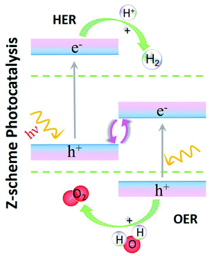 |
| | Fig. 1 Schematic of Z-scheme photocatalysis. | |
In this article, we have presented an exhaustive comparative study of MoS2 and MoSSe based vdW HTSs, where the second layer is from the family of (i) TMDs, viz. WS2, HfS2, ZrS2, TiS2 and (ii) TMOs, viz. HfO2, T-PtO2, T-SnO2. The existing literature so far has not discussed the above listed vdW HTS configurations for Z-scheme photocatalysis. Up to this date, earlier reports exist only on monolayers of type II vdW HTSs of TMDs and TMOs for photocatalytic applications.52 Here, using state-of-the-art theoretical methodologies within the framework of hybrid density functional theory (DFT) and many body perturbation theory (MBPT) (viz. G0W0) we have systematically studied the important parameters for photocatalytic applications. First, we introduce the different possible stable configurations of vdW HTSs. Next, we discuss the band edge alignment of 2D monolayers and their corresponding vdW HTSs. Subsequently, their recombination path is thoroughly analyzed to check their capabilities as Z-scheme photocatalysts. Finally, their accurate optical responses are computed and understood using the MBPT technique for considering them for photocatalytic devices. Strikingly, we observe that, despite most of the individual monolayers not performing optimally as photocatalysts, their vdW HTSs with type II band edge alignment appear to be efficient Z-scheme photocatalysts.
2 Methodology
We have employed a first-principles based methodology under the framework of DFT.53–58 PAW pseudopotentials are used in our calculations using the plane wave basis set as employed in the Vienna ab initio simulation package (VASP).59–61 The exchange–correlation (xc) interactions amongst electrons are accounted for by the generalized gradient approximation (GGA) with the functional form as proposed by Perdew–Burke–Ernzerhof (PBE).62,63 The hybrid density functional has also been employed to account for the same with the functional proposed by Heyd–Scuseria–Ernzerhof (HSE06).64 The hybrid functional (HSE06) considers 25% mixing (α) of the short range Hartree–Fock (HF) exchange. Its long range part is described by the GGA-PBE functional.
The vdW HTSs are optimized using the PBE functional and HSE06 is used to determine the single point energy. The conjugate gradient minimization is performed with the Brillouin zone (BZ) sampling of a 2 × 2 × 1 K-grid and the energetics are obtained by the BZ sampling of a 16 × 16 × 1 K-grid. An energy tolerance of 0.001 meV and a force tolerance of 0.001 eV Å−1 have been used for optimization. In the ground state calculations, the plane wave cut-off energy is set to 600 eV. The vdW HTSs are modelled with a 20 Å vacuum in order to avoid electrostatic interactions between the periodic images. The two-body vdW interaction as devised by Tkatchenko–Scheffler has been employed.65,66 The correction parameter is based on Hirshfeld partitioning of the electron density. Note that we have not included spin–orbit coupling (SOC) in our calculations, since the previous literature has reported only a slight change in the band gap due to this.44,67,68 The optical properties are calculated using the GW approach.69,70 We have performed hybrid calculations (HSE06) as an initial step for single shot GW calculations (i.e. G0W0@HSE06).
3 Results and discussion
3.1 Heterostructure stacking
We have constructed commensurate bilayer vdW HTSs71 with minimum lattice mismatch between the layers. The vdW HTSs have been formed with a monolayer of MoS2 (or MoSSe) and a monolayer of WS2, ZrS2, HfS2, TiS2, HfO2, T-PtO2 or T-SnO2, in vertical alignment. The specifications of the monolayers (see the lattice parameters in ESI†) corroborate with the existing literature.52,72,73 All of the monolayers constitute a 2 × 2 × 1 supercell (24 atoms) except ZrS2 and HfS2, where the  supercell consists of 21 atoms. Here, the stacking styles between the two monolayers have not been varied in each vdW HTS. This is due to the fact that a binding energy change of merely a few meV is observed with the change in stacking styles of the two monolayers in a particular vdW HTS.74,75
We have calculated the binding energy of vdW HTSs by the expression,74
| | Eb = E(vdW HTSs) − E(MoS2![[thin space (1/6-em)]](https://www.rsc.org/images/entities/char_2009.gif) orMoSSe) − E(BX2) orMoSSe) − E(BX2) | (1) |
where
Eb is the binding energy of the vdW HTS MoS
2/BX
2 (or MoSSe/BX
2),
E(MoS
2) is the energy of monolayer MoS
2,
E(MoSSe) is the energy of monolayer MoSSe and
E(BX
2) is the energy of monolayer BX
2 (where B = W, Hf, Zr, Pt or Sn and X = S or O).
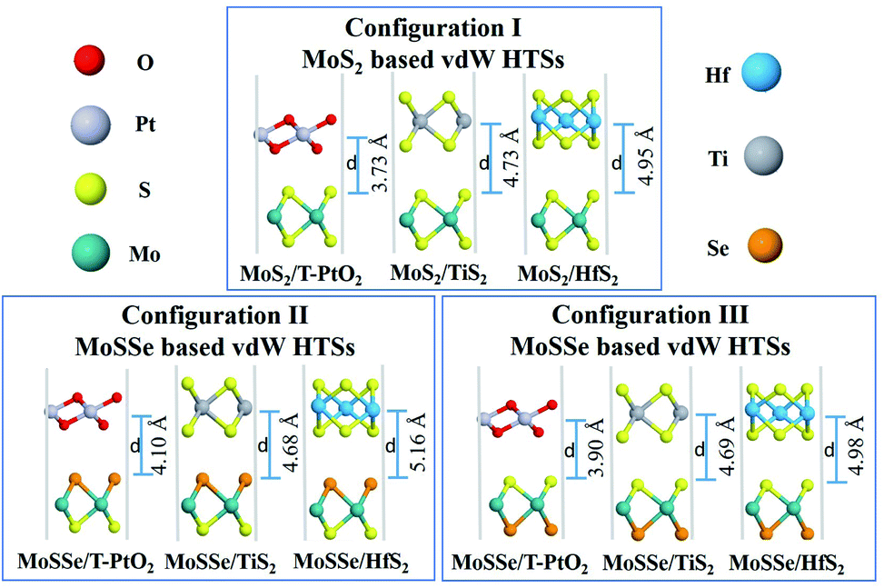
Fig. 2 shows the three configurations of vdW HTSs considered in the present work. Configuration I is of the type MoS2/BX2. The stacking type of MoS2/T-SnO2, MoS2/ZrS2 and MoS2/WS2(or HfO2) are the same as that of MoS2/T-PtO2, MoS2/HfS2 and MoS2/TiS2, respectively. By replacing MoS2 with MoSSe, we have created configurations II and III. The former consists of a Se atomic layer from MoSSe at the interface, whereas the latter has a S atomic layer at the interface. Configurations II and III also follow the same pattern as configuration I. Table 1 contains the lattice mismatches and the binding energies of all of the vdW HTS configurations. We define the mismatch as (l(MoS2) − l(BX2))/l(BX2), where l(MoS2) and l(BX2) are the lattice constants of MoS2 and BX2, respectively.
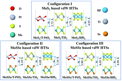 |
| | Fig. 2 vdW HTSs with configurations I, II and III. MoS2/BX2 (configuration I), MoSSe/BX2 (configuration II), where the Se atomic layer is at the interface, and MoSSe/BX2 (configuration III), where the S atomic layer is at the interface. | |
Table 1 The corresponding bilayer vdW HTS lattice mismatches and binding energies of the different configurations (MoS2/BX2(I), MoSSe/BX2(II and III))
| BX2 |
Lattice mismatch (%) |
Binding energy (eV) |
| I |
II |
III |
| WS2 |
0.0 |
−1.04 |
−1.05 |
−1.02 |
| ZrS2 |
2.5 |
−0.49 |
−0.54 |
−0.52 |
| HfS2 |
3.9 |
−0.30 |
−0.35 |
−0.33 |
| TiS2 |
2.5 |
−0.45 |
−1.00 |
−0.94 |
| HfO2 |
1.2 |
−0.40 |
−0.54 |
−0.47 |
| T-PtO2 |
0.4 |
−0.83 |
−0.63 |
−0.68 |
| T-SnO2 |
1.8 |
−2.19 |
−2.24 |
−2.22 |
3.2 Band edge alignment
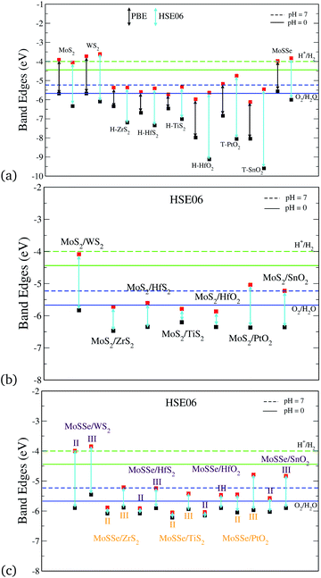
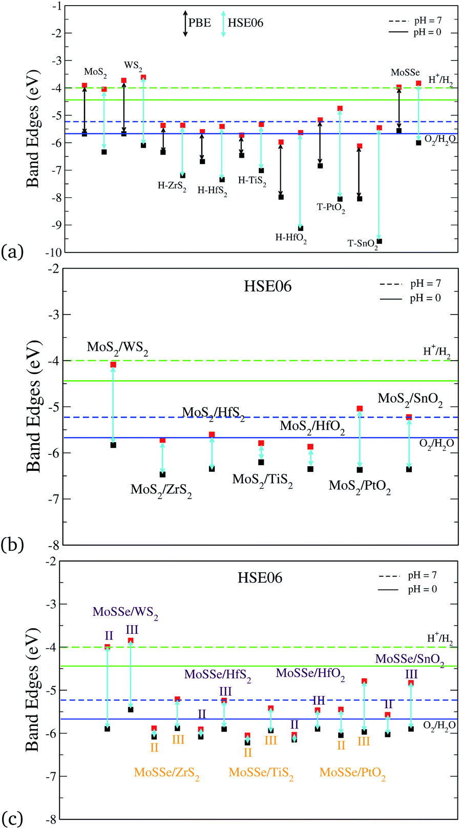
Photocatalytic applications require the understanding of the band gaps and absolute band edge positions. We have calculated these with both the PBE and HSE06 functionals. Fig. 3(a) shows the band edge alignments of the monolayers. We observe here that the chosen monolayers for the vdW HTSs have type II heterojunctions. In Fig. 3, H+/H2 and O2/H2O correspond to the reduction and oxidation potentials of water splitting, respectively, for both pH(0) (solid line) and pH(7) (dashed line). Fig. 3(a) shows that HSE06 and PBE have some discrepancies in estimating the band edge positions. Calculations with the HSE06 functional incorporate the HF exact exchange term resulting due to the self-interaction error of e−, which is not well taken care of in the case of the PBE functional. Hence, the results presented in further plots are carried out using the HSE06 functional.
 |
| | Fig. 3 Band edge alignment with respect to water redox potentials of (a) the individual monolayers, (b) MoS2/BX2 vdW HTSs (configuration I), (c) MoSSe/BX2 vdW HTSs (configuration II and III), where BX2 refers to WS2, ZrS2, HfS2, TiS2, HfO2, PtO2 or SnO2. | |
Fig. 3(b) and (c) depict the absolute band edge positions of the MoS2 and MoSSe based vdW HTSs, respectively. Fig. 3(b) indicates that individual band alignment approximately predicts the combined alignment of the vdW HTSs. The weak vdW interactions between the 2D monolayers is attributed to the aforementioned prediction. Here, type II alignment can be seen with the VBM of the MoS2 (or MoSSe) monolayer and the CBM of HfS2, ZrS2, TiS2, HfO2, T-PtO2 and T-SnO2 monolayers. The band gaps of the monolayers and vdW HTSs are listed in the ESI† (Table II). The CBM and VBM should lie a few eVs above and below the redox potentials of water for the material to be suitable for photocatalysis. However, in our case the vdW HTSs band gaps do not straddle the photocatalytic water splitting potentials. Hence, we analyze these bilayer vdW HTSs for their applicability as Z-scheme photocatalysts. The vdW HTSs selected for further analysis from Fig. 3 are the configurations consisting of HfS2, ZrS2, TiS2, HfO2, T-PtO2 and T-SnO2. Note that the MoS2 (or MoSSe) monolayer (CBM) does form type II alignment with WS2 (VBM) as well and the HTS is observed to be capable of photocatalysis (but not via the Z-scheme). However, we have included this in our manuscript as a reference, with an intention to showcase a clear distinction with regards to Z-scheme photocatalysts. Moreover, from observing Fig. 3(c) a unanimously similar trend suggests that the band gaps of the vdW HTSs with configuration II are significantly different than those with configuration III.
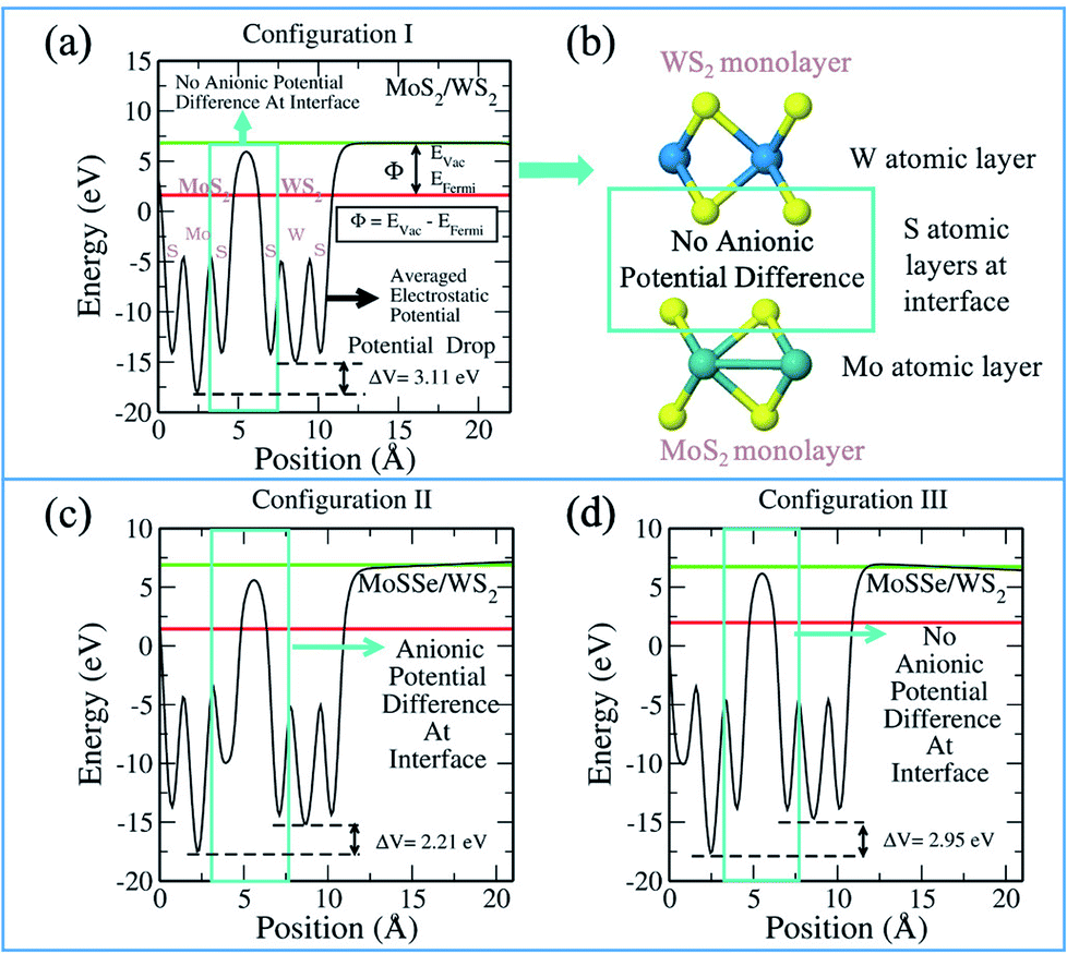
It should be noted that the absolute band edge alignment is obtained with respect to the zero vacuum level. The associated EVac (vacuum level) of each calculation is obtained from the electrostatic potential of the system. As is evident from the term, the plot explains the electrostatic potential corresponding to each atomic layer (see Fig. 4). It is pertinent to understand the plot as it informs us about the work function and potential difference between the monolayers. Thus, we are able to analyze the interlayer charge transfer that indicates the photocatalytic ability. Fig. 4 presents the electrostatic potential plot of MoS2/WS2. From left to right in Fig. 4(a), we observe the potential of the S, Mo and S atomic layers of the MoS2 monolayer and the S, W and S atomic layers of the WS2 monolayer. We see a clear difference in the potentials of the cationic layers with regards to the Mo and W atomic layers. The gradient between the monolayers facilitates the charge separation between them. Fig. 4(b) shows the corresponding MoS2/WS2 vdW HTS, describing the respective atomic layers.
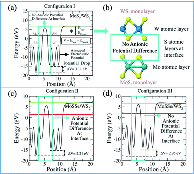 |
| | Fig. 4 Electrostatic potential plot of MoS2/WS2 depicting (a) potential difference in configuration I, (b) schematic of configuration I; (c) potential difference in configuration II and (d) potential difference in configuration III. | |
Fig. 4(c) and (d), show the plots for MoSSe/WS2 configuration II and III, respectively. We observe that in configuration II (Fig. 4(c)) there is an additional potential gradient between the Se atomic layer of MoSSe and the S atomic layer of the WS2 at the interface, along with the cationic potential difference. In the case of configuration III, the interface has no anionic gradient (due to the presence of S in both of the layers facing each other) and hence, charge separation is mainly the result of the cationic gradient. Therefore, we see different band gaps in configuration III and configuration II. Further, one should always remember, that these configurations are type II and the band edge levels are on two different layers. Therefore, any potential gradient at the interface will definitely effect the corresponding band edge levels. Fig. S1–S6 in ESI† discuss the electrostatic potentials for other vdW HTSs. Fig. S4† explains the change in the band gap on the basis of the dipole direction. The dipole direction is seen from S to Se i.e. from the lower to the higher potential. So, we observe opposite dipole directions in configurations II and III, thereby affecting the interfacial interactions. Thus, the vdW HTSs with TMOs are also in line with the above discussion and inference.
We have also calculated the associated charge densities on the layers and the work functions of the vdW HTSs. The work function (ϕ) is a significant parameter to understand the charge separation or transfer at the interface. It is defined as follows:
where
EVac and
EFermi are the electrostatic potentials corresponding to the vacuum level and Fermi level, respectively (see
Fig. 4).
Table 2 gives the total Hirshfeld charges (of all of the atoms in the monolayers of the HTSs) and the work functions of vdW HTSs. The estimated values of the work functions of the free standing monolayers (
ϕM as in
Table 3), corroborate with the existing literature.
73‡ The Hirshfeld charge in the case of configuration II shows greater charge transfer than those of configuration I and III. This is attributed to the anionic and cationic potential difference at the interface. The smaller charge transfer corresponds to the lower work function in configurations I and III. The plane averaged charge density difference Δ
ρ has been calculated (see Section V in the ESI
†) by:
| | | Δρ = ρ(vdW HTSs) − ρ(MoS2 or MoSSe) − ρ(BX2) | (3) |
where
ρ(vdW HTSs),
ρ(MoS
2),
ρ(MoSSe) and
ρ(BX
2) are the charge densities of the vdW HTS, monolayer MoS
2, monolayer MoSSe and monolayer BX
2, respectively.
Table 2 The Hirshfeld charges and work functions of the different configurations (I: MoS2/BX2, II: MoSSe/BX2 (Se interfacial layer), III: MoSSe/BX2 (S interfacial layer))
| BX2 |
Hirshfeld charge (e) |
Work function (ϕ) (eV) |
| I |
II |
III |
I |
II |
III |
| WS2 |
0.64 |
0.19 |
3.00 |
5.19 |
5.34 |
4.76 |
| ZrS2 |
−0.26 |
−0.25 |
−0.16 |
5.98 |
6.02 |
5.56 |
| HfS2 |
−0.08 |
−0.14 |
−0.07 |
5.98 |
6.01 |
5.58 |
| TiS2 |
−0.09 |
−0.25 |
−0.12 |
6.02 |
6.15 |
5.69 |
| HfO2 |
−0.04 |
−0.12 |
−0.09 |
6.12 |
6.13 |
5.70 |
| T-PtO2 |
0.03 |
−0.08 |
−0.04 |
5.78 |
5.75 |
5.53 |
| T-SnO2 |
−0.10 |
−0.16 |
−0.06 |
5.91 |
5.79 |
5.46 |
We can understand the charge transfer by calculating the band bending (ΔEBB) as well. This parameter is estimated by the Fermi-level difference between the vdW HTSs and the corresponding free-standing monolayer, with the expression as follows:76
where
ϕ is the work function of the vdW HTS and
ϕM is the work function of the free standing monolayer. A Δ
EBB < 0 indicates charge transfer from the vdW HTSs to the monolayer. All of the vdW HTSs display Δ
EBB < 0
i.e. charge is gained by the monolayer (
Table 3). The observation is in agreement with the calculated Hirshfeld charges as noted in
Table 2. It is to be noted that in the case of WS
2, Δ
EBB is more negative, with
ϕM(MoS
2) = 5.82 eV compared to
ϕM(WS
2). Hence, the associated Hirshfeld charge on the WS
2 monolayer is positive. The above observations indicate that the MoSSe based configurations (II and III) can play a crucial role in photocatalytic applications.
Table 3 The estimated band bending between vdW HTSs and the free-standing monolayer (ϕM is the work function of the free standing monolayer, I: MoS2/BX2, II: MoSSe/BX2 (Se interfacial layer), III: MoSSe/BX2 (S interfacial layer))
| BX2 |
ϕ
M (eV) |
ΔEBB (eV) |
| I |
II |
III |
| WS2 |
5.53 |
−0.34 |
−0.19 |
−0.77 |
| ZrS2 |
6.95 |
−0.97 |
−0.93 |
−1.39 |
| HfS2 |
7.13 |
−1.15 |
−1.12 |
−1.55 |
| TiS2 |
7.01 |
−0.99 |
−0.86 |
−1.32 |
| HfO2 |
8.86 |
−2.74 |
−2.73 |
−3.16 |
| T-PtO2 |
7.86 |
−2.08 |
−2.11 |
−2.33 |
| T-SnO2 |
9.06 |
−3.15 |
−3.27 |
−3.60 |
The aforementioned discussions, along with Fig. 3(a), have showcased the spatial charge separation due to the work function difference. Therefore, with the e−–h+ pair generation in the individual monolayers of the vdW HTSs, the MoS2 (or MoSSe) monolayer will be positively charged as it contributes to the VBM of the vdW HTS, which will restrict the flow of e− to the other layer (BX2). Moreover, the BX2 monolayer that contributes to the CBM of the vdW HTS does not straddle the reduction potential. Hence, the MoS2 (or MoSSe) monolayer will have restricted e− motion from its CBM to the BX2 CBM, thereby facilitating the e−–h+ recombination path of the BX2 CBM to the MoS2 VBM and promoting the standard Z-scheme mechanism.
3.3 Recombination in vdW HTSs
Considering the case of photocatalysts that straddle the potentials, less recombination is synchronous with effective photocatalytic capability. However, for their applicability as Z-scheme photocatalysts, higher recombination is required in the vdW HTSs compared to their constituent monolayers. Hence, the layer with a CBM above the reduction potential can facilitate HER, while the layer with a VBM below the oxidation potential can facilitate OER. In view of this, we have analyzed the recombination rate, which is indicated by the effective mass of the electrons and holes. The effective mass have been calculated by the parabolic fitting at the CBM and VBM in the band structures obtained by the hybrid calculations.77 The band structures of MoS2/ZrS2 have been previously reported78 and are in agreement with those reported in the present work. The same data for the other vdW HTSs discussed here are previously unreported.
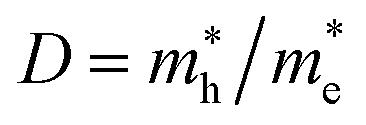
The recombination in the system can be estimated by relative ratio (D) that is defined as follows:79
| |  | (5) |
The higher the variance of D from 1, the less the recombination. Since, D refers to the relative ratio of the effective mass of holes  and electrons
  a value closer to 1 (i.e. a low variance) is ideal for high recombination in the system . This is obvious as a value closer to 1 indicates similar electron and hole effective mass, resulting in easier recombination. On the contrary, a large difference in the effective mass leads to significant differences in the carrier mobilities, leading to the separation of carriers and hindrance of their recombination. Consider Tables 4 and 5 that gives the value of D for the monolayers and their corresponding vdW HTSs, respectively. The effective mass of carriers at the CBM (i.e.
 ) and VBM (i.e.
 ) have been obtained along the designated direction in the high symmetry path Γ–M–K–Γ (see the band structures i.e. Fig. S7 in the ESI†). Also, it should be noted that the parameter is calculated from the band structures of the supercells rather than the primitive cells. Since the supercell is small, the density of the bands near the VBM and CBM is not very high and hence the band folding is not an issue here.
Table 4 The effective mass ratios (D) of the monolayers (BX2) except for MoS2 and MoSSe (both have same value of D = 1.21)
| BX2 |
WS2 |
ZrS2 |
HfS2 |
TiS2 |
HfO2 |
T-PtO2 |
T-SnO2 |
|
D
|
1.29 |
1.58 |
1.17 |
0.03 |
5.88 |
4.66 |
9.00 |
Table 5 The effective mass ratios (D) of the vdW HTSs (I: MoS2/BX2, II: MoSSe/BX2 (Se interfacial layer), III: MoSSe/BX2 (S interfacial layer))
| BX2 |
Effective mass ratio (D) |
| I |
II |
III |
| WS2 |
2.50 |
0.85 |
10.19 |
| ZrS2 |
0.13 |
0.64 |
0.62 |
| HfS2 |
0.65 |
0.87 |
0.71 |
| TiS2 |
0.50 |
0.20 |
0.80 |
| HfO2 |
0.32 |
0.34 |
0.34 |
| T-PtO2 |
0.49 |
0.50 |
0.49 |
| T-SnO2 |
0.91 |
1.15 |
1.14 |
Furthermore, since we are considering Z-scheme photocatalysis, we require monolayers with less recombination compared to that of their corresponding vdW HTSs. In order to review this, we have checked the variance of the D values for the monolayers and the vdW HTSs. Therefore, the vdW HTSs with D values which have a smaller variance compared to those of their respective monolayers can be considered probable Z-scheme photocatalysts. As per the discussed approach, we have deduced MoSSe/ZrS2 (configuration II and III), MoSSe/HfS2 (configuration II), MoSSe/TiS2 (configuration III), MoS2/SnO2 and MoSSe/SnO2 (configuration II and III) as probable Z-scheme vdW HTSs. Amongst these, the D values for MoS2/SnO2, MoSSe/HfS2 (configuration II) and MoSSe/TiS2 (configuration III) show the smallest variance. Their respective carrier mobilities80 are computed as 46 × 102 cm2 V−1 s−1, 21 × 102 cm2 V−1 s−1 and 2 × 102 cm2 V−1 s−1. Additional details are provided in the ESI.† Note that, we have also estimated their exciton binding energies (EB), and the vdW HTSs showed comparatively smaller EB as compared to those of the MoS2 and MoSSe monolayers (see Section VII in the ESI†). It should be mentioned here that the value of D is an indicative approach and should not be considered as the sole criterion for e−–h+ recombination. This yields future scope to explore the carrier dynamics more to understand the excitonic physics in these materials. We have, nevertheless, supported the inferences with the study of the optical responses, carrier mobilities, H2O adsorption and HER.
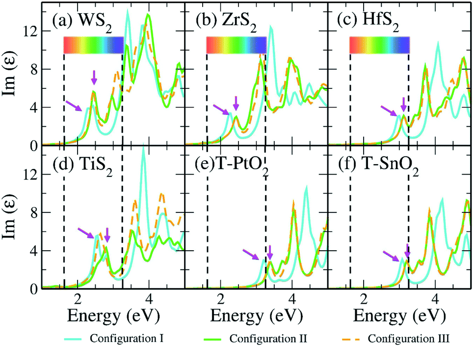
3.4 Absorption spectra
Optical response is amongst the important parameters involved in constructing photocatalytic devices. Therefore, we have obtained the absorption spectra for the previously discussed vdW HTSs that can be considered for photocatalytic applications. Fig. 5 gives the absorption spectra obtained from the imaginary part of the dielectric function as computed by the GW method (G0W0@HSE06). The dielectric function is a frequency dependent complex function (ε(ω) = Re(ε) + Im(ε)) where the real part (Re(ε)) is computed from the Kramers–Kronig relation, and the imaginary part (Im(ε)) is obtained from the interband matrix elements in the momentum space.81 Since the interband process consists of transitions to the unoccupied orbitals, the Im(ε) gives the absorption spectra. The first peak will, therefore, indicate the onset of the absorption process. We observe that the vdW HTSs of MoS2/TMD and MoS2/TMO have responses in the visible region. The spectra corresponding to the MoSSe vdW HTSs (configuration II and III) have shown minute blue shifts compared to those of the MoS2 vdW HTSs. Furthermore, we observe from Fig. 5 that the vdW HTSs with ZrS2 (Fig. 5b) and TiS2 (Fig. 5d) monolayers show red shifts compared to the other vdW HTSs (i.e., Fig. 5(a), (c), (d)–(f)). The spectra thus indicate the use of MoS2/ZrS2, MoSSe/ZrS2, MoS2/TiS2 and MoSSe/TiS2 for harnessing the overlap region of Im(ε) with the solar spectrum in order to construct photocatalytic devices.
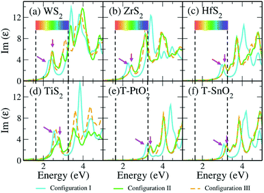 |
| | Fig. 5 Imaginary part of the dielectric function vs. energy plot depicting the optical responses of the vdW HTS configurations I, II and III by G0W0@HSE06. Here, the arrows indicate the initial peak positions that are associated with the absorption onset. | |
3.5 H2O adsorption
We have further calculated the H2O adsorption in these vdW HTSs to confirm that the adsorption is supported for further redox reactions. The associated expression is given as:| | | Eads = E(adsorbed H2O) − E(vdW HTSs) − E(H2O) | (6) |
where Eads is the adsorption energy (see Table 6) of the H2O on the vdW HTSs, E(adsorbed H2O) is the energy of the vdW HTSs with adsorbed H2O, E(vdW HTSs) is the energy of the vdW HTSs and E(H2O) is the energy of the water molecule. From Table 6 we observe that H2O is physisorbed in the system and its binding strength in all of the monolayers is higher than that of WS2. Also, the transition metal oxides show higher binding strengths than the transition metal dichalcogenides. The data supplements the previous analysis which supports considering the monolayers for Z-scheme photocatalysis.
Table 6 H2O adsorption on the monolayer surfaces
| BX2 |
Adsorption energy (eV) |
Distance (Å) |
| WS2 |
−0.09 |
2.88 |
| ZrS2 |
−0.24 |
2.59 |
| HfS2 |
−0.23 |
2.75 |
| TiS2 |
−0.25 |
2.74 |
| T-PtO2 |
−0.28 |
2.08 |
| T-SnO2 |
−0.29 |
2.31 |
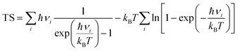
In addition, we have calculated the Gibbs free energy changes (ΔG) of the intermediate in the HER as per the expression:
where Δ
E is the intermediate adsorption energy on the vdW HTSs, Δ
Ezpe is the change in zero-point energy and Δ
S is the difference in entropy. The temperature,
T, is taken as 300K. We have calculated the
Ezpe and TS by the following expression using density functional perturbation theory (DFPT):
| |  | (8) |
| |  | (9) |
where ℏ is Planck’s constant,
νi is the vibrational frequency and
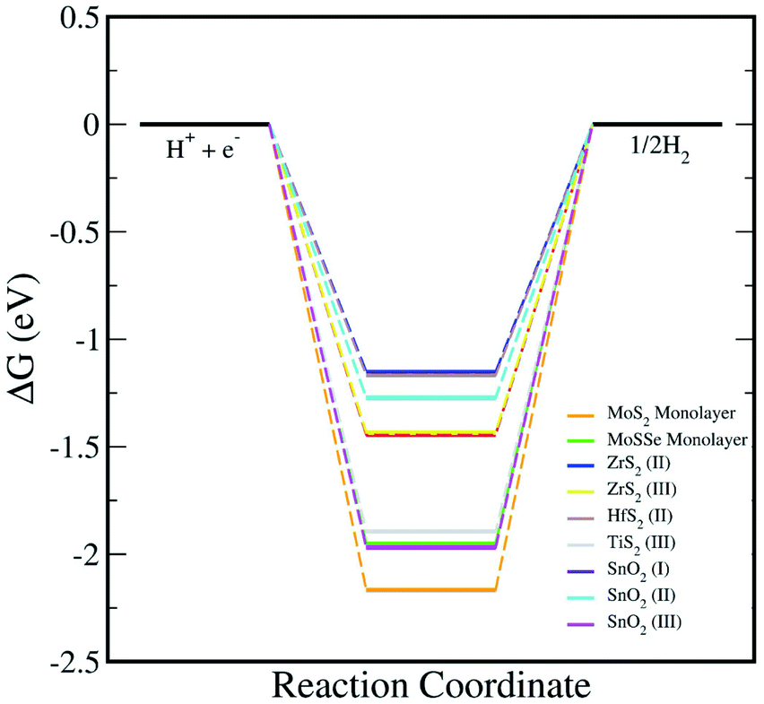
kB is the Boltzmann constant. The HER diagram along the reaction pathway H
+ + e
− → H* → 1/2H
2 is illustrated in
Fig. 6. Here, H* represents the adsorbed intermediate. Under the conditions of pH = 0 and a standard hydrogen electrode (SHE) potential of 0 V, H
+ + e
− is equivalent to the 1/2H
2.
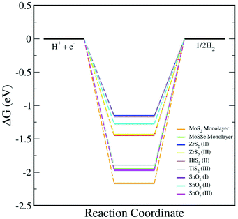 |
| | Fig. 6 The HER reaction free energy diagrams on the monolayers and vdW HTSs at an electrode potential ESHE = 0 V and pH = 0. At zero potential, (H+ + e−) can be expressed as 1/2H2. | |
Now, upon systematically revisiting all of the aforementioned factors, we have observed vdW HTSs to have type II band alignment with their work function being affected by the interfacial potential difference. This further influences the charge separation. Another point is that the smaller conduction band offset between the two monolayer systems would promote efficient charge separation at the interface.82 Therefore, in reference to Fig. 3, with the comparatively large differences in the two conduction band levels along with type II alignment, the possibility of interlayer recombination in vdW HTSs for the Z-scheme process seems very plausible. Effective mass is also an important factor for this, and we have indicated the recombination probability by the effective mass ratio (D). However, since this approach is qualitative, we have explicitly included the results of the optical responses, H2O adsorption and HER as direct evidence to validate MoSSe/HfS2, MoSSe/TiS2, MoS2/T-SnO2, MoSSe/T-SnO2 and MoSSe/ZrS2 as probable Z-scheme photocatalysts.
4 Conclusion
An exhaustive study has been undertaken for understanding different MoS2 and MoSSe based vdW HTSs. As per the band edge alignment, it is observed that these vdW HTSs do not facilitate the normal photocatalytic process as the band edges do not straddle the redox potential. However, they are predicted to show Z-scheme photocatalysis. The band edge alignments of the MoSSe vdW HTSs infer larger band gaps in configuration III than in configuration II. This has been attributed to the additional anionic potential gradient due to the Se atomic layer at the interface in configuration II. The probability of recombination, as suggested by the effective mass ratio (D), has corroborated MoSSe/HfS2, MoSSe/TiS2, MoS2/T-SnO2, MoSSe/T-SnO2 and MoSSe/ZrS2 as favourable Z-scheme photocatalysts. The absorption spectra further confirm the visible light response of these vdW HTSs and hence, their applicability in photocatalytic devices. Finally, the H2O adsorption and HER indicate their interactions with water to help the photocatalytic process.
Conflicts of interest
There are no conflicts of interest to declare.
Acknowledgements
AS thanks IIT Delhi for the financial support. AS and MJ thank Pooja Basera for the helpful discussions. MJ acknowledges CSIR, India, for the senior research fellowship [grant no. 09/086(1344)/2018-EMR-I]. SB acknowledges the financial support from SERB under the Core Research Grant [CRG/2019/000647]. We thank the High Performance Computing (HPC) facility at IIT Delhi for computational resources.
Notes and references
- M. Ni, M. K. Leung, D. Y. Leung and K. Sumathy, Renewable Sustainable Energy Rev., 2007, 11, 401–425 CrossRef CAS.
- H. Yao, M. Fan, Y. Wang, G. Luo and W. Fei, J. Mater. Chem. A, 2015, 3, 17511–17524 RSC.
- F. Opoku, K. K. Govender, C. G. C. E. van Sittert and P. P. Govender, New J. Chem., 2017, 41, 11701–11713 RSC.
- C. Yu, F. Chen, D. Zeng, Y. Xie, W. Zhou, Z. Liu, L. Wei, K. Yang and D. Li, Nanoscale, 2019, 11, 7720–7733 RSC.
- A. Gupta, T. Sakthivel and S. Seal, Prog. Mater. Sci., 2015, 73, 44–126 CrossRef CAS.
- A. Singh, P. Basera, S. Saini, M. Kumar and S. Bhattacharya, J. Phys. Chem. C, 2020, 124, 1390–1397 CrossRef CAS.
- Y. Chen, S. Huang, X. Ji, K. Adepalli, K. Yin, X. Ling, X. Wang, J. Xue, M. Dresselhaus and J. Kong,
et al.
, ACS Nano, 2018, 12, 2569–2579 CrossRef CAS PubMed.
- C. Rao, K. Gopalakrishnan and U. Maitra, ACS Appl. Mater. Interfaces, 2015, 7, 7809–7832 CrossRef CAS PubMed.
- E. Singh, P. Singh, K. S. Kim, G. Y. Yeom and H. S. Nalwa, ACS Appl. Mater. Interfaces, 2019, 11, 11061–11105 CrossRef CAS PubMed.
- H. Zeng, G.-B. Liu, J. Dai, Y. Yan, B. Zhu, R. He, L. Xie, S. Xu, X. Chen and W. Yao,
et al.
, Sci. Rep., 2013, 3, 1608 CrossRef PubMed.
- C.-Y. Wang and G.-Y. Guo, J. Phys. Chem. C, 2015, 119, 13268–13276 CrossRef.
- N. Glebko, I. Aleksandrova, G. C. Tewari, T. S. Tripathi, M. Karppinen and A. J. Karttunen, J. Phys. Chem. C, 2018, 122, 26835–26844 CrossRef CAS.
- K. W. Lau, C. Cocchi and C. Draxl, Phys. Rev. Mater., 2019, 3, 074001 CrossRef CAS.
- M. Mattinen, G. Popov, M. Vehkama ki, P. J. King, K. Mizohata, P. Jalkanen, J. Ra isa nen, M. Leskela and M. Ritala, Chem. Mater., 2019, 31, 5713–5724 CrossRef CAS.
- S. Lebègue, T. Björkman, M. Klintenberg, R. M. Nieminen and O. Eriksson, Phys. Rev. X, 2013, 3, 031002 Search PubMed.
- J. Yang, Z. Zeng, J. Kang, S. Betzler, C. Czarnik, X. Zhang, C. Ophus, C. Yu, K. Bustillo and M. Pan,
et al.
, Nat. Mater., 2019, 18, 970–976 CrossRef CAS PubMed.
- C. C. Leong, H. Pan and S. K. Ho, Phys. Chem. Chem. Phys., 2016, 18, 7527–7534 RSC.
- P. Liao and E. A. Carter, Chem. Soc. Rev., 2013, 42, 2401–2422 RSC.
- L. Ju, M. Bie, J. Shang, X. Tang and L. Kou, J. Phys.: Mater., 2020, 3, 022004 CAS.
- Y. Sun, Z. Shuai and D. Wang, Nanoscale, 2018, 10, 21629–21633 RSC.
- B. Song, L. Liu and C. Yam, J. Phys. Chem. Lett., 2019, 10, 5564–5570 CrossRef CAS PubMed.
- M. Sun and U. Schwingenschlogl, Chem. Mater., 2020, 32, 4795–4800 CrossRef CAS.
- X. Ma, X. Wu, H. Wang and Y. Wang, J. Mater. Chem. A, 2018, 6, 2295–2301 RSC.
- Y. Luo, S. Wang, H. Shu, J.-P. Chou, K. Ren, J. Yu and M. Sun, Semicond. Sci. Technol., 2020, 35, 125008 CrossRef CAS.
- A. Kuc and T. Heine, Chem. Soc. Rev., 2015, 44, 2603–2614 RSC.
- R. Kumar, I. Verzhbitskiy, F. Giustiniano, T. P. Sidiropoulos, R. F. Oulton and G. Eda, 2D Mater., 2018, 5, 041003 CrossRef CAS.
- Y. Huang, X. Chen, C. Wang, L. Peng, Q. Qian and S. Wang, Nanoscale, 2017, 9, 8616–8622 RSC.
- H. Terrones, F. López-Urías and M. Terrones, Sci. Rep., 2013, 3, 1549 CrossRef PubMed.
- Q. Zhang and U. Schwingenschlögl, Phys. Rev. B: Condens. Matter Mater. Phys., 2018, 97, 155415 CrossRef CAS.
- P. Rivera, K. L. Seyler, H. Yu, J. R. Schaibley, J. Yan, D. G. Mandrus, W. Yao and X. Xu, Science, 2016, 351, 688–691 CrossRef CAS PubMed.
- P. Li, W. Zhang, D. Li, C. Liang and X. C. Zeng, ACS Appl. Mater. Interfaces, 2018, 10, 19897–19905 CrossRef CAS PubMed.
- P. Li, W. Zhang, C. Liang and X. C. Zeng, Nanoscale, 2019, 11, 19806–19813 RSC.
- Y. Luo, K. Ren, S. Wang, J.-P. Chou, J. Yu, Z. Sun and M. Sun, J. Phys. Chem. C, 2019, 123, 22742–22751 CrossRef CAS.
- Y. Luo, S. Wang, K. Ren, J.-P. Chou, J. Yu, Z. Sun and M. Sun, Phys. Chem. Chem. Phys., 2019, 21, 1791–1796 RSC.
- K. Ren, S. Wang, Y. Luo, J.-P. Chou, J. Yu, W. Tang and M. Sun, J. Phys. D: Appl. Phys., 2020, 53, 185504 CrossRef CAS.
- S. Wang, C. Ren, H. Tian, J. Yu and M. Sun, Phys. Chem. Chem. Phys., 2018, 20, 13394–13399 RSC.
- Y. Li, Y.-L. Li, C. M. Araujo, W. Luo and R. Ahuja, Catal. Sci. Technol., 2013, 3, 2214–2220 RSC.
- E. Parzinger, B. Miller, B. Blaschke, J. A. Garrido, J. W. Ager, A. Holleitner and U. Wurstbauer, ACS Nano, 2015, 9, 11302–11309 CrossRef CAS PubMed.
- Z.-K. Tang, W.-J. Yin, L. Zhang, B. Wen, D.-Y. Zhang, L.-M. Liu and W.-M. Lau, Sci. Rep., 2016, 6, 32764 CrossRef CAS PubMed.
- X. Gao, Y. Shen, Y. Ma, S. Wu and Z. Zhou, Appl. Phys. Lett., 2019, 114, 093902 CrossRef.
- R. Zhang, L. Zhang, Q. Zheng, P. Gao, J. Zhao and J. Yang, J. Phys. Chem. Lett., 2018, 9, 5419–5424 CrossRef CAS PubMed.
- K. Ren, C. Ren, Y. Luo, Y. Xu, J. Yu, W. Tang and M. Sun, Phys. Chem. Chem. Phys., 2019, 21, 9949–9956 RSC.
- B.-J. Wang, X.-H. Li, R. Zhao, X.-L. Cai, W.-Y. Yu, W.-B. Li, Z.-S. Liu, L.-W. Zhang and S.-H. Ke, J. Mater. Chem. A, 2018, 6, 8923–8929 RSC.
- C.-F. Fu, Q. Luo, X. Li and J. Yang, J. Mater. Chem. A, 2016, 4, 18892–18898 RSC.
- Y. Liu, X. Zeng, C. D. Easton, Q. Li, Y. Xia, Y. Yin, X. Hu, J. Hu, D. Xia and D. T. McCarthy,
et al.
, Nanoscale, 2020, 12, 8775–8784 RSC.
- X. Xia, M. Song, H. Wang, X. Zhang, N. Sui, Q. Zhang, V. L. Colvin and W. Y. William, Nanoscale, 2019, 11, 11071–11082 RSC.
- K. Maeda, ACS Catal., 2013, 3, 1486–1503 CrossRef CAS.
- H. Li, W. Tu, Y. Zhou and Z. Zou, Adv. Sci., 2016, 3, 1500389 CrossRef PubMed.
- A. J. Bard, J. Photochem., 1979, 10, 59–75 CrossRef CAS.
- J. Lang and Y. H. Hu, Phys. Chem. Chem. Phys., 2020, 22, 9250–9256 RSC.
- L. Ju, Y. Dai, W. Wei, M. Li and B. Huang, Appl. Surf. Sci., 2018, 434, 365–374 CrossRef CAS.
- F. A. Rasmussen and K. S. Thygesen, J. Phys. Chem. C, 2015, 119, 13169–13183 CrossRef CAS.
-
R. M. Martin, Electronic structure: basic theory and practical methods, Cambridge university press, 2004 Search PubMed.
-
R. M. Martin, L. Reining and D. M. Ceperley, Interacting Electrons, Cambridge University Press, 2016 Search PubMed.
- C. Freysoldt, B. Grabowski, T. Hickel, J. Neugebauer, G. Kresse, A. Janotti and C. G. Van de Walle, Rev. Mod. Phys., 2014, 86, 253 CrossRef.
- L.-p. Feng, J. Su, S. Chen and Z.-t. Liu, Mater. Chem. Phys., 2014, 148, 5–9 CrossRef CAS.
- P. Hohenberg and W. Kohn, Phys. Rev., 1964, 136, B864 CrossRef.
- W. Kohn and L. J. Sham, Phys. Rev., 1965, 140, A1133 CrossRef.
- G. Kresse and J. Furthmüller, Phys. Rev. B: Condens. Matter Mater. Phys., 1996, 54, 11169 CrossRef CAS PubMed.
- P. E. Blöchl, Phys. Rev. B: Condens. Matter Mater. Phys., 1994, 50, 17953 CrossRef PubMed.
- V. Blum, R. Gehrke, F. Hanke, P. Havu, V. Havu, X. Ren, K. Reuter and M. Scheffler, Comput. Phys. Commun., 2009, 180, 2175–2196 CrossRef CAS.
- C. Stampfl and C. Van de Walle, Phys. Rev. B: Condens. Matter Mater. Phys., 1999, 59, 5521 CrossRef CAS.
- J. P. Perdew, K. Burke and M. Ernzerhof, Phys. Rev. Lett., 1996, 77, 3865 CrossRef CAS PubMed.
- J. Heyd, G. E. Scuseria and M. Ernzerhof, J. Chem. Phys., 2003, 118, 8207–8215 CrossRef CAS.
- A. Tkatchenko and M. Scheffler, Phys. Rev. Lett., 2009, 102, 073005 CrossRef PubMed.
- A. Tkatchenko, R. A. DiStasio Jr, R. Car and M. Scheffler, Phys. Rev. Lett., 2012, 108, 236402 CrossRef PubMed.
- J. Weng and S.-P. Gao, Phys. Chem. Chem. Phys., 2018, 20, 26453–26462 RSC.
- K. Ren, W. Tang, M. Sun, Y. Cai, Y. Cheng and G. Zhang, Nanoscale, 2020, 12, 17281–17289 RSC.
- G. Onida, L. Reining and A. Rubio, Rev. Mod. Phys., 2002, 74, 601 CrossRef CAS.
- H. Jiang, P. Rinke and M. Scheffler, Phys. Rev. B: Condens. Matter Mater. Phys., 2012, 86, 125115 CrossRef.
- A. U. Rahman, J. M. Morbec, G. Rahman and P. Kratzer, Phys. Rev. Mater., 2018, 2, 094002 CrossRef CAS.
- C. M. Bastos, R. Besse, J. L. Da Silva and G. M. Sipahi, Phys. Rev. Mater., 2019, 3, 044002 CrossRef CAS.
- S. Haastrup, M. Strange, M. Pandey, T. Deilmann, P. S. Schmidt, N. F. Hinsche, M. N. Gjerding, D. Torelli, P. M. Larsen and A. C. Riis-Jensen,
et al.
, 2D Mater., 2018, 5, 042002 CrossRef CAS.
- C. Xia, W. Xiong, W. Xiao, J. Du, L. Fang, J. Li and Y. Jia, Phys. Rev. Appl., 2018, 10, 024028 CrossRef CAS.
- X. Hu, L. Kou and L. Sun, Sci. Rep., 2016, 6, 31122 CrossRef CAS PubMed.
- J. Padilha, A. Fazzio and A. J. da Silva, Phys. Rev. Lett., 2015, 114, 066803 CrossRef CAS PubMed.
- A. Ganose, A. Jackson and D. Scanlon, J. Open Source Softw., 2018, 3, 717 CrossRef.
- A. K. A. Lu, M. Houssa, M. Luisier and G. Pourtois, Phys. Rev. Appl., 2017, 8, 034017 CrossRef.
- H. Zhang, L. Liu and Z. Zhou, RSC Adv., 2012, 2, 9224–9229 RSC.
- J. Dai and X. C. Zeng, Angew. Chem., 2015, 127, 7682–7686 CrossRef.
- P. Basera, S. Saini and S. Bhattacharya, J. Mater. Chem. C, 2019, 7, 14284–14293 RSC.
- S. Khanchandani, P. K. Srivastava, S. Kumar, S. Ghosh and A. K. Ganguli, Inorg. Chem., 2014, 53, 8902–8912 CrossRef CAS PubMed.
Footnotes |
| † Electronic supplementary information (ESI) available. See DOI: 10.1039/d1na00154j |
| ‡ Note that the mentioned reference has considered a 15 Å vacuum, whereas we have used a 20 Å vacuum. The slight differences (i.e. the not exact matches) may be due to this change. |
|
| This journal is © The Royal Society of Chemistry 2021 |
Click here to see how this site uses Cookies. View our privacy policy here. 
 Open Access Article
 This Open Access Article is licensed under a Creative Commons Attribution-Non Commercial 3.0 Unported Licence
 *,
Manjari
Jain
*,
Manjari
Jain

 supercell consists of 21 atoms. Here, the stacking styles between the two monolayers have not been varied in each vdW HTS. This is due to the fact that a binding energy change of merely a few meV is observed with the change in stacking styles of the two monolayers in a particular vdW HTS.74,75
 and electrons
  a value closer to 1 (i.e. a low variance) is ideal for high recombination in the system . This is obvious as a value closer to 1 indicates similar electron and hole effective mass, resulting in easier recombination. On the contrary, a large difference in the effective mass leads to significant differences in the carrier mobilities, leading to the separation of carriers and hindrance of their recombination. Consider Tables 4 and 5 that gives the value of D for the monolayers and their corresponding vdW HTSs, respectively. The effective mass of carriers at the CBM (i.e.
 ) and VBM (i.e.
 ) have been obtained along the designated direction in the high symmetry path Γ–M–K–Γ (see the band structures i.e. Fig. S7 in the ESI†). Also, it should be noted that the parameter is calculated from the band structures of the supercells rather than the primitive cells. Since the supercell is small, the density of the bands near the VBM and CBM is not very high and hence the band folding is not an issue here.