
 Open Access Article
 This Open Access Article is licensed under a
 Creative Commons Attribution 3.0 Unported Licence
Energetic carbon precursors for micro-supercapacitor printing†
Christin
Gellrich
,
Stefanie
Lochmann
,
Thomas
Otto
,
Julia
Grothe
and
Stefan
Kaskel
 *
*
TU Dresden, Institute of Inorganic Chemistry, Bergstraße 66, 01069 Dresden, Germany. E-mail: Stefan.kaskel@tu-dresden.de
First published on 24th August 2021
Abstract
A highly energetic carbon precursor suitable for soft lithographic processing based on acetylene dicarboxylic acid is presented. High-resolution micro-supercapacitors with line width down to 500 nm are produced using solvent assisted nanoimprint lithography. The resulting nonporous carbons exhibit remarkably low specific resistance down to 6.9 × 10⁻⁵ Ω m pyrolyzed at 800 °C. The interdigital electrodes show excellent device capacitances of up to 1.32 mF cm−2 with an average capacitance retention of 97% after 10![[thin space (1/6-em)]](https://www.rsc.org/images/entities/char_2009.gif) 000 cycles. Tailoring the performance is achieved by variation of electrode distances and carbonization temperatures.
000 cycles. Tailoring the performance is achieved by variation of electrode distances and carbonization temperatures.
Introduction
The establishment of portable electronic devices in medicine, technical applications and consumer electronics also attracted an immense attention in research of miniaturized modules. Pursuing this objective, recent efforts in nanotechnology and the development of maintenance-free microelectronics such as autonomous micro-sensors or medical implants and nanorobotics also stimulated the development of micro-scale energy storage units.1–5 In this sense micro-supercapacitors with remarkable power densities, fast charge/discharge rates and ultra-long cycle life assembled on ultra-small device areas are extensively studied.6,7 A wide range of different surface structuring and electrode deposition techniques are established and approaches concerning simple, lightweight packaging and leakage safety are investigated.8–10 Prominent methods for producing interdigital electrodes are for example direct laser writing,11,12 inkjet printing10,13,14 or stamping and screen printing.15–17 Recently used inks include carbon materials like graphene and graphene oxide,10,18,19 CNTs20 as well as MXenes.14,17,21Nanoimprint lithography (NIL) is a promising technique for the production of high-resolution interdigital carbon elec-trodes.22,23 The approach is using liquid carbon precursors and enables binder free direct printing of precursor structures. After pyrolysis the porous carbon electrodes adhere to the substrate. Compared to, for example, photolithographic techniques, the nanoimprint lithography facilitates fast and low-cost printing and high process throughput. A typical limiting resolution achieved via soft lithographic techniques using PDMS as stamping material is around 200 nm.24,25
The ongoing trend towards ever smaller mobile devices forces the development of flexible, stretchable and transparent devices.26 Especially in the production of e-skin, wearable devices or biomedical applications a high degree of shape stability and elasticity is required.13,27,28 In this sense polymer or silicon substrates are used to produce micro-supercapacitors.29 However, printing carbon precursors onto flexible substrates requires carbonization temperatures significantly above the melting point of the substrate.29 Hence, for porous carbon printing applications precursors transforming into conductive carbons at low temperatures are required.
Typical flexible substrates consist of polyimide (Kapton), PET or PDMS.8,30–32 The carbon properties like electronic conductivity and porosity are highly dependent on the carbonization temperature.33 Provided that the electronic conductivity has a decisive influence on the performance of high-resolution micro-supercapacitors, the formation of a suitable carbon material with high electronic conductivity and appropriate surface area remains to be a challenge. Graphene and other particle dispersions afford high surface areas when deposited on substrates but continuous processing via printing technologies is hampered by clogging of nozzles and stamps.
Micro-structuring provides a good accessibility and an increased carbon surface area can even be achieved without porous carbons. A challenge is to envision molecular precursors graphitizable at low temperature (<900 °C). In this regard, energetic carbon precursors based on alkynes are promising candidates. Acetylene is a widely used gaseous precursor for CNT production and CVD processes. It is a carbon rich molecule, promising for the formation of graphitic carbon structures.34–36 For the processing of a liquid carbon precursor additional functional groups like carboxylate groups are ideal as the CO2 elimination is favorable. In this sense we envisioned acetylene dicarboxylic acid to be an ideal precursor for micro-contact printing. In the following we present an acetylene dicarboxylic acid-based carbon precursor for the nanoimprint processing of micro-supercapacitor with a high resolution in-plane interdigital structure (Fig. 1).
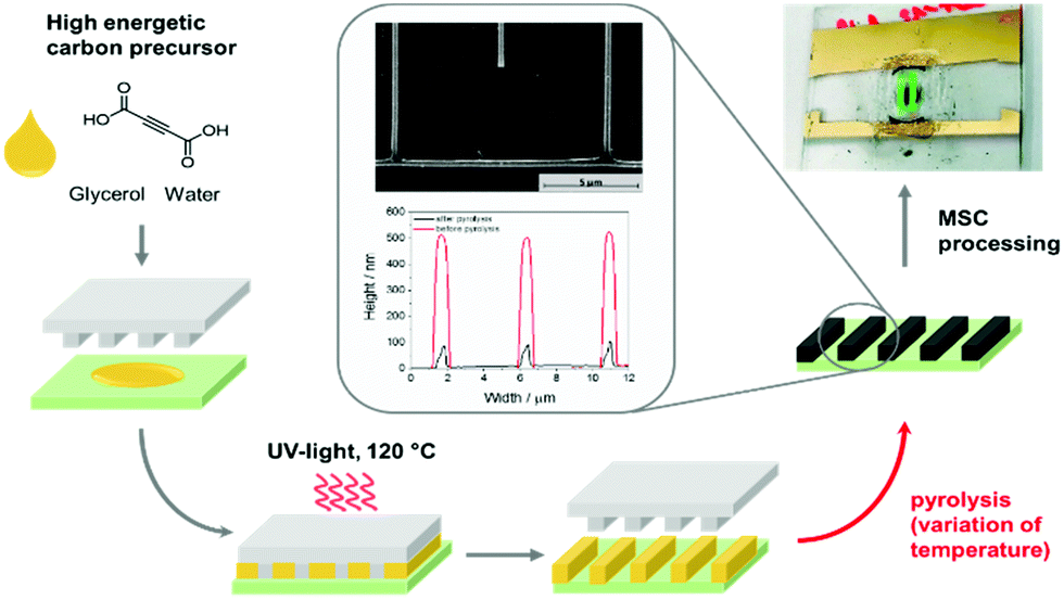 | ||
| Fig. 1 Schematic procedure of the SA-NIL process using a high energetic carbon precursor and further MSC processing. | ||
Results and discussion
A new energetic carbon precursor system is developed to produce in-plane micro-supercapacitors (MSC) with interdigital geometry using the solvent assisted nanoimprint lithography (SA-NIL) technique (Fig. 1).A suitable precursor must fulfill various requirements regarding processability and shape stability. The selected solvent system should have a high vapor pressure to ensure a fast curing under thermal or UV-treatment, forming the desired homogeneous and stable pattern. The main focus is to reduce the necessary carbonization temperature significantly below 900 °C and guarantee a high electrical conductivity at the same time.
We study a promising energy-rich carbon precursor based on acetylene dicarboxylic acid (H2ADC), glycerol and sulfuric acid. During pattering of the mixture, the structure is cured through polymerization triggered by heating and UV-radiation. Three different interdigital structures are tested and compared using the same line height of 500 nm but different line width of 10 μm (IDE 500/10), 5 μm (IDE 500/5) and 1 μm (IDE 500/1). The influence of the carbonization temperature on the material and structural characteristics like conductivity, porosity and line heights as well as the electrochemical performance are explored.
Precursor characterization
The processability of the dissolved acetylene dicarboxylic acid is increased using glycerol as esterification agent in order to obtain a more homogeneous precursor. At the same time, the polymerization of these educts is promising to form stable structures during NIL-printing.In our work, the triol glycerol serves as an optimal polymerization agent. To characterize and optimize the polymerization and esterification degree, various heat and UV-radiation treatments are analyzed by infrared spectroscopy (Fig. 2a). The treated and untreated acid-alcohol mixtures exhibit very similar IR-spectra showing mainly the characteristic stretches of the pure dicarboxylic acid and glycerol. These are namely the valence and deformation vibration of the OH-groups (∼3400 cm−1) and the characteristic vibration of the carboxyl-group at 1650 cm−1 caused by the acid, glycerol and 20 wt% of water.
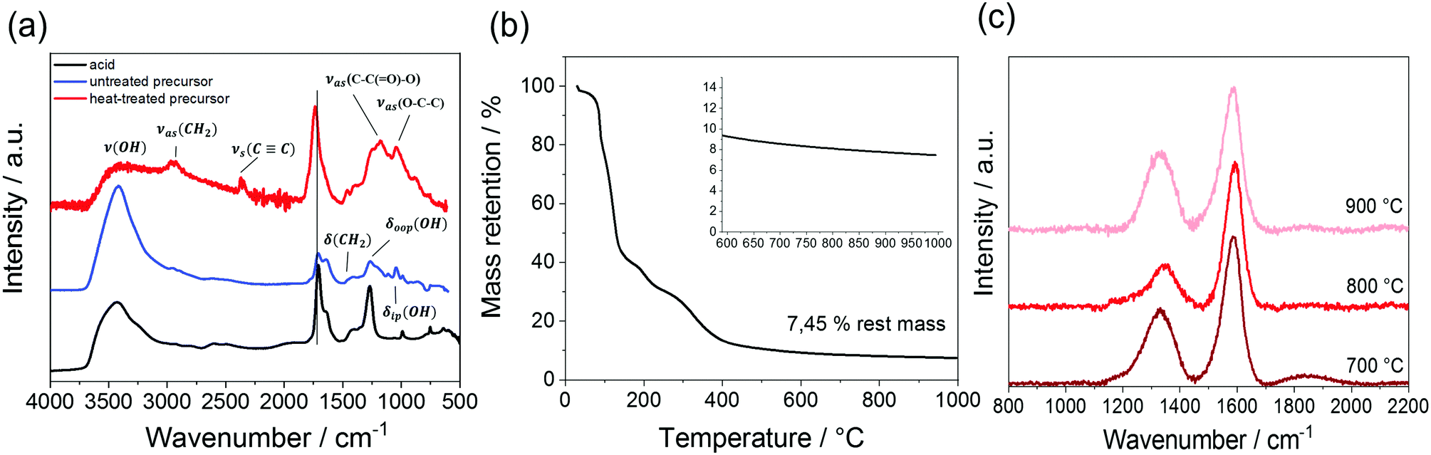 | ||
| Fig. 2 IR-spectra of the pure acid (black line), the untreated (blue line) and treated precursor (red line) (a), thermal analysis (b), Raman-spectra of the precursor powders carbonized at 700 °C, 800 °C and 900 °C in Ar-atmosphere (c). | ||
To enhance the polymerization, concentrated sulfuric acid is added to the solution, treated again with UV-light and cured at 100 °C afterwards. In the polymerized system the two characteristic bands of the ester groups are clearly visible (νas(C–C(![[double bond, length as m-dash]](https://www.rsc.org/images/entities/char_e001.gif) O)–O) at 1250 cm−1 and νas(O–C–C) at 1080 cm−1). Furthermore, due to the formation of the ester, the symmetric valence stretch of the C
O)–O) at 1250 cm−1 and νas(O–C–C) at 1080 cm−1). Furthermore, due to the formation of the ester, the symmetric valence stretch of the C![[triple bond, length as m-dash]](https://www.rsc.org/images/entities/char_e002.gif) C triple bond at 2300 cm−1 clearly emerges, because the symmetry of H2ADC is reduced and the stretch of the CC triple bond becomes IR-active. A slight shift in the stretch of the carboxylic group to higher wavenumbers can be recognized and is now observed at 1710 cm−1, the typical range for the CO vibration in the alpha-beta unsaturated ester group (usually at 1750–1715 cm−1).37,38
C triple bond at 2300 cm−1 clearly emerges, because the symmetry of H2ADC is reduced and the stretch of the CC triple bond becomes IR-active. A slight shift in the stretch of the carboxylic group to higher wavenumbers can be recognized and is now observed at 1710 cm−1, the typical range for the CO vibration in the alpha-beta unsaturated ester group (usually at 1750–1715 cm−1).37,38
The TG measurements suggest that a temperature of 450 °C is sufficient to completely transform the organic precursor, because at higher temperatures only a small mass loss is observed (Fig. 2b).
To characterize the surface properties of the material, nitrogen physisorption and Raman measurements are performed using the carbon powder carbonized at varying temperature. Therefore, carbon powders are prepared at carbonization temperatures between 500 to 900 °C. The powders show no appreciable specific surface area at all analyzed pyrolysis temperatures, indicating a total absence of porosity. In the Raman spectra, the presence of highly graphitic carbon, carbonized at temperatures between 700 to 900 °C under Argon, can be observed. Due to the high reactivity, even conversion temperatures as low as 300 °C in air are sufficient to produce this allotrope of carbon (ESI,† Fig. S1). This observation is in agreement with observations by Bourlinos et al., who investigated the formation of a carbonaceous solid after pyrolysis of monopotassium salt of acetylene dicarboxylic acid at 300 °C. Besides the characteristic D-band at 1350 cm−1 for disordered carbon structures, the G-band at 1595 cm−1 assigned to the graphitic carbon is present,37 rendering the precursor as promising for the transformation into materials for electrochemical energy storage (Fig. 2c). The powder carbonized at 800 °C showed the lowest ratio of ID/IG with 0.28 and therefore the highest amount of graphitic carbon, followed by 700 °C (0.50) and 900 °C (0.54). The drop of the ID/IG ratio at 900 °C is probably caused by the increasing degradation of the carbon material at high temperatures.
The electrochemical properties of the carbon material are investigated using compact thin films after different carbonization temperatures between 600 and 900 °C (Table 1). As expected, the electrical conductivity increases with increasing temperatures due to a higher graphitization.39 The lowest resistance is achieved for the sample carbonized at 800 °C with 6.92 × 10⁻⁵ Ωm due to the highest amount of graphitic carbon at this temperature. The specific resistance for the sample prepared at 900 °C is slightly higher probably due to the increasing carbon degradation and possible cracking occurring especially at high temperatures. A dramatic increase in the resistance emerges at temperatures below 700 °C.
| Temperature [°C] | Resistance [kΩ] | Film thickness [nm] | Specific resistance [Ω m] |
|---|---|---|---|
| 600 | 87.5 × 10³ | 820 | 71.75 |
| 700 | 6.850 | 640 | 4.384 × 10⁻³ |
| 800 | 0.407 | 170 | 6.919 × 10⁻⁵ |
| 900 | 0.330 | 450 | 1.485 × 10⁻⁴ |
After processing at 600 °C the material showed unacceptably low conductivity. The loss of conductivity could be caused by the minimal increase of organic residues in the material, which probably have a high impact on the overall resistance. However, the compact thin films pyrolyzed at 800 °C and 700 °C showed remarkably low specific resistances which are about three times lower than for comparable carbon precursors at those temperatures.40 Therefore, we focused especially on pyrolysis temperatures between 700 and 900 °C for the subsequent preparation of micro-supercapacitors.
Nanoimprint lithography
Due to the promising results of the powder characterization, the precursor was applied in the nanoimprint process. In general, the generation of homogeneous crack-free and completely separated electrode fingers is a crucial requirement to obtain high performance interdigital electrodes. The nanoimprint lithography is a suitable procedure to generate high-resolution structures. The short distances between the electrodes, created with this technique, are an important factor to accelerate the ion transport and reduce the diffusion resistance. In this work, we present the printing of high-resolution interdigital micro-structures with line widths of 500 nm and distances down to only 1 μm using the investigated energy-rich carbon precursor. The characteristic structure parameters are summarized in Table 2.| Structure | Line width [nm] | Distance [μm] | Finger length [μm] |
|---|---|---|---|
| IDE 500/10 | 500 | 1 | 400 |
| IDE 500/5 | 500 | 5 | 400 |
| IDE 500/1 | 500 | 10 | 400 |
The precursor is an ideal candidate for application of the SA-NIL process, because, using water as solvent, it provides an ideal viscosity and curability at moderate temperatures and UV-radiation.
After the printing process at 120 °C, lines with heights of around 500 nm are produced (Fig. 3). The etching depth of the stamp is 500 nm. Typically, the line height is lower than this value because the solvent is evaporated during printing. In this case, it indicates significant swelling of the printed lines at high humidity. Only for the IDE 500/10 the line height is lower with 380 nm. In the subsequent SEM image precursor droplets along the patterned lines are visible, which might promote emergence of short circuits in the final MSCs. The formation of droplets together with the swelling of the lines is caused by the hydrophilic nature of the precursor and is especially occurring when the structures are stored at room temperature. To prevent these side effects and the appearance of short circuits of electrodes, the structures should be stored at 120 °C before carbonization.
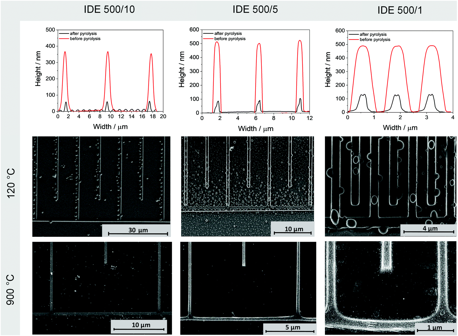 | ||
| Fig. 3 Height profiles (after printing red lines (polymer), after pyrolysis black lines (carbon)) of the different structures and SEM images of the three different structures after printing at 120 °C and after carbonization at 900 °C. | ||
After pyrolysis at 900 °C, almost no residues between the lines are visible, but a homogenous pattern with clearly separated and completely contacted electrode fingers is observed. During the pyrolysis high volume shrinkage and height loss of the lines down to 60–140 nm occurs. The average line height, which was achieved for all structures and all temperatures, allows an electrochemical application. Interestingly, a layered structural characteristic of the resulting carbon material can be observed in the SEM image (Fig. 3) for the pyrolyzed IDE 500/1 structure indicating the formation of graphitic domains.
In analogy to the structures pyrolyzed at 900 °C, carbonization temperatures of 800 °C and 700 °C are analyzed. Theoretically, an increase in the achieved line heights due to the decrease of graphitization is expected. However, no remarkable line height and width differences could be observed probably because the graphitization state is still very high at these temperature ranges (ESI,† Fig. S2), making the precursor an interesting material for further electrochemical applications.
Electrochemical characterization
To analyze the basic electrochemical behavior of the carbon bulk material compact thin films and sandwich type EDLCs are prepared and investigated (Fig. 4). For the precursor pyrolyzed at 900 °C, a high specific areal capacitance of 14.8 mF cm−2 is reached. The system shows a low internal series resistance of 5 Ω, which underlines the high conductivity of the carbon. Compared to that, the carbon material pyrolyzed at 800 °C reaches an areal capacitance of 5.3 mF cm−2.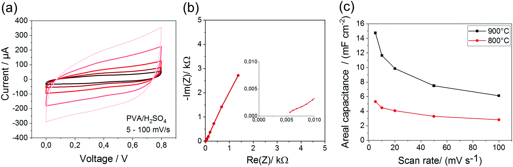 | ||
| Fig. 4 Electrochemical characterization of the thin film EDLC (CV-curves) (a), GCD-curves (b), Nyquist plot (c). | ||
The interdigital MSCs are electrochemically characterized using a PVA/H2SO4-electrolyte. In Fig. 5, these results are shown for the IDE 500/10 exemplarily as well as for the IDE 500/5 and IDE 500/1 (ESI,† Fig. S4) all pyrolyzed at 900 °C.
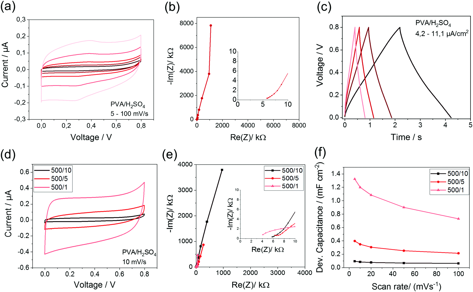 | ||
| Fig. 5 Electrochemical characterization of IDE 500/10 pyrolyzed at 900 °C (CV-curves (a), Nyquist plot (b), GCD-curves (c)) and of the three different structures (CV-curves (d), Nyquist plot (e), device Capacitances (f)). | ||
The CV-curves of all analyzed structures show a characteristic rectangular shape even at high scan rates. The Nyquist plot exhibits the typical form, which is expected for capacitive systems. The ESR (equivalent series resistance) ranges between 4–6 kΩ and is much higher compared to the thin film EDLCs caused by the small line width of the interdigital structure. Theoretically, it is expected that the capacitance increases with smaller electrode distances, because of smaller diffusion pathways. This trend can also be seen for the analyzed geometries. Here, the IDE 500/1 shows with 1.32 mF cm−2 the highest device capacitance in comparison to the device capacitance of IDE 500/5 with 0.40 mF cm−2 and IDE 500/10 with 0.1 mF cm−2. Due to the lowest distance, IDE 500/1 shows the lowest diffusion resistance and therefor exhibits the lowest ESR with only 4 kΩ. Surprisingly, very high device capacitances for all structures could be reached, despite the porosity and specific surface area of the carbon material is moderate. This underlines the importance of the implementation of a highly conductive material as electrode material to achieve high capacitances, which greatly compensates a possible absence of a high surface area carbon. Moreover, the high-resolution pattern increases the outer surface area and the accessibility of the electrodes. Furthermore, the influence of the carbonization temperature on the electrochemical performance are investigated. The calculated device capacitances for all structures at different carbonization temperatures are shown in Table 3.
| Temperature [°C] | IDE 500/10 [mF cm−2] | IDE 500/5 [mF cm−2] | IDE 500/1 [mF cm−2] |
|---|---|---|---|
| 900 | 0.10 | 0.40 | 1.32 |
| 800 | 0.16 | 0.04 | 0.48 |
| 700 | 0.18 | 0.02 | 0.22 |
Because the IDE 500/1 exhibits the highest capacitance, the CV-curves, Nyquist plots and rate capability of the three analyzed temperatures are shown in detail in Fig. 6a–c. As expected, the capacitances decrease with lower carbonization temperatures, because the graphitization and therefore conductivity decreases. Because of the absence of porosity an effect on the capacitance with temperature change can be neglected. The mentioned trend can be seen for the IDE 500/5 structure as well (Fig. 6d).
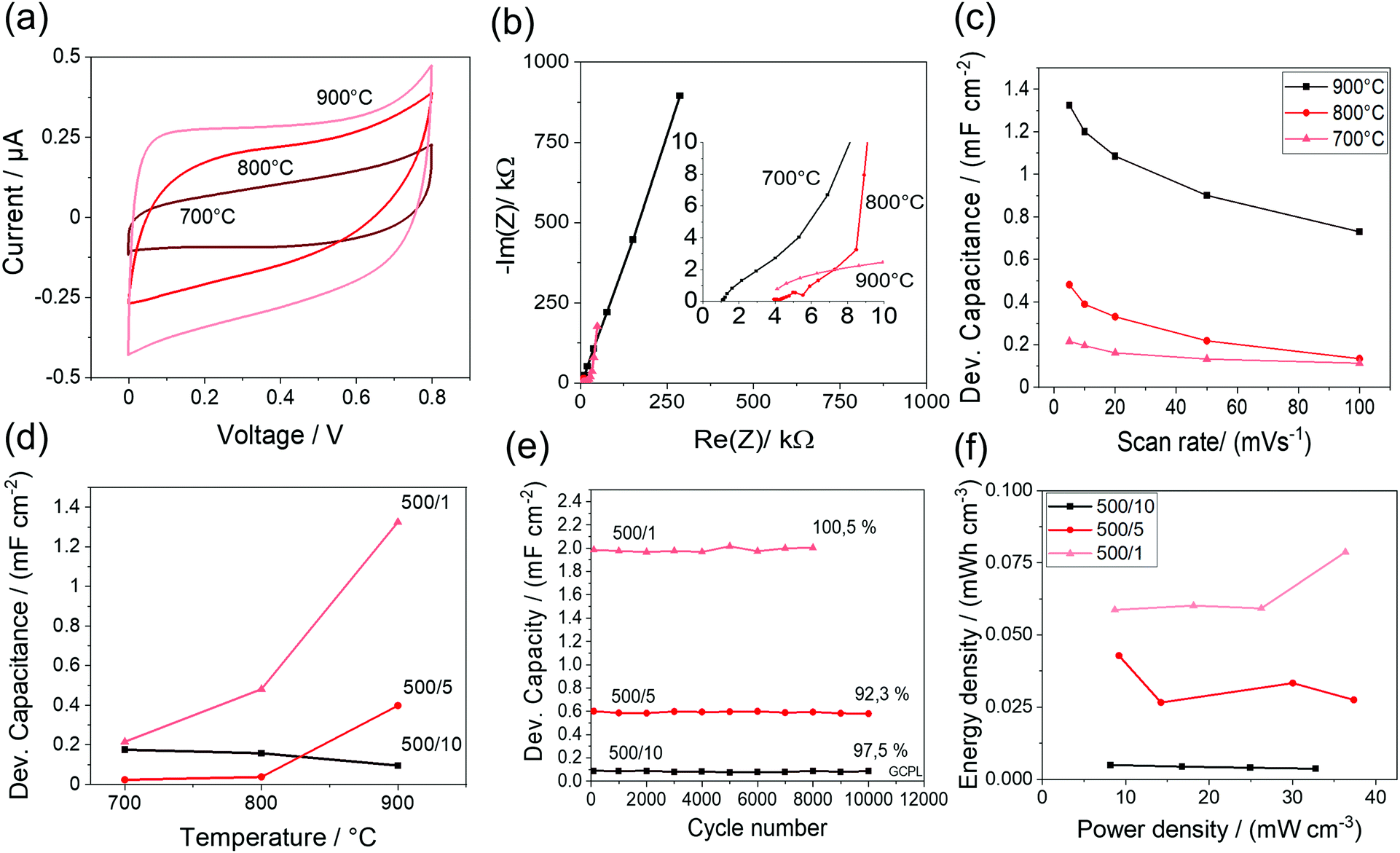 | ||
| Fig. 6 Electrochemical characterization of the IDE 500/1 at different temperatures (CV-curves (a), Nyquist plot (b), rate capability (c); device capacitances of all structures at different temperatures (d), GCD cycling stability over 10000 cycles at 8.3 μA cm−2 for all structures (e) and the Ragone plot (f) both for 900 °C pyrolysis temperature). | ||
However, beyond the discussed temperature influence, the fabrication of defect-free structures without cracks after carbonization is another crucial challenge to achieve high capacitances. This might cause the observed reverse trend for the IDE 500/10, where the probability of line cracks is lower at reduced temperatures.
The electrode distance might play another important role when it comes to the fabrication of defect free MSCs. The interdigital structure with the smallest electrode distance (IDE 500/1) shows the highest number of electrode fingers and therefore the highest probability of line cracks and contact problems, which makes a fabrication of defect free MSCs with reproducible device capacitances more challenging. This influence, and the mentioned influence of lower conductivity, might cause the device capacitance drop from 900 °C to 800 °C for the IDE 500/1. However, high device capacitances for all structures could be reached.
To analyze the cycling stability of the fabricated MSCs, 10000 charge and discharge cycles are performed (Fig. 6e). For all structures, an excellent cycling stability could be observed, leading to a maximal capacity retention of 92%. In the Ragone plot (Fig. 6f), all structures pyrolyzed at 900 °C showed similar power densities at different scan rates from 4.2 to 11.1 μA cm−2, because all structures exhibit the same line width of 500 nm. However, the energy densities could be significantly improved with decreasing line distances and transport pathways, because of decreasing diffusion path length. Therefore, IDE 500/1 showed the highest energy density with an average of 0.07 mW h cm−3.
Experimental
Precursor preparation
The carbon precursor is synthesized using 0.340 g (2.981 mmol) of acetylene dicarboxylic acid (97%, abcr GmbH) and 0.276 g (2.981 mmol) of glycerol (Carl Roth) solved in 0.16 ml deionized water. To improve the polymerization, 32.4 mg of sulfuric acid (95%, Sigma Aldrich) is added.Compact film formation
The thin films are prepared on pre-treated boro-aluminium silicate slides (Corning 1737, DELTA Technologies) (25 mm × 25 mm × 1.1 mm). In the pre-treatment step, the slides are stored in piranha solution (1 part 30% H2O2, 3 parts conc. H2SO4) for at least 30 minutes, cleaned with deionized water and ethanol and dried in a nitrogen stream afterwards. Furthermore, the surface of the dried substrate is activated in argon plasma (kiNPen, Neoplas Tools). Thin films are formed by spin coating (Spin 150, ATP GmbH) 80 μl of the carbon precursor applied on the substrate using a speed of 2000 rpm for 30 seconds. The thin films are dried at 100 °C and pyrolyzed in a tube furnace at temperatures between 300 and 900 °C with a heating rate of 150 K min−1 for 2 h under argon stream.Preparation of thin film supercapacitors
To prepare layered EDLCs the pyrolyzed compact films are placed in acetone in order to separate them from the substrate and dried at 70 °C. The two electrodes are coated with electro-conductive varnish (electro-DAG) and afterwards with the dried films. To activate the electrodes, they are treated at 80 °C in vacuum overnight before additionally activation with Ar-plasma. Afterwards, the hydrogel electrolyte is added (see electrolyte synthesis) and a polypropylene separator placed between the electrolyte layers. After drying both electrodes at 45 °C they are built together in a Swagelok setup.Nanoimprint lithography
For the synthesis of interdigital patterned structures the solvent assisted nanoimprint lithography is applied using a micro-contact-printing System μ-CP 3.0 (GeSim mbH). The substrate-material and its pre-treatment is analogous to the compact films. The preparation of the patterned PDMS stamps (Sylgard 184 elastomer kit, Dow Chemicals) is described elsewhere.41 A droplet of 4 μl precursor is applied onto the substrate before the stamp is pressed into it in order to fill the space in the stamp pattern. To receive an adequate solvent removal, the printing is carried out under constant pressure of 165 kPa and temperature of 120 °C for 900 seconds. For an improved polymerization and curing of the precursor, the structure is irradiated with UV-light during the whole printing process. After peeling of the stamp, the structure is dried at 100 °C and pyrolyzed at the same conditions as the carbon films. In this work, three different interdigital structures are prepared with line widths of 10 μm (IDE-1), 5 μm (IDE-2) and 1 μm (IDE-3) and maximum line heights and widths of 500 nm each. The structures are analyzed by atomic force microscopy (Dimensions D 3100, Digital Instruments) and SEM (DSM-982 Gemini, Zeiss) measurements.Electrolyte synthesis
The used proton conductive electrolyte is a polymer hydrogel consisting of a mixture of polyvinyl alcohol (PVA; Merck; molecular weight 145000) and sulfuric acid in a ratio of 1:1.2. For an optimal amount 1 g of PVA (0.0069 mol) is added to 14 ml deionized water and heated at 90 °C under constant stirring and reflux. Afterwards 1.2 g (0.0122 mol) conc. sulfuric acid is added drop-wise so that a clear gel-like solution is created.
Preparation of interdigital micro-supercapacitors and electrochemical characterization
Possibly attached carbon residues are carefully removed before the interdigital structure is covered with silicone to protect it from the following deposition of a chrome (10 nm) and gold (100 nm) current collector. The physical vapor deposition (B39, Malz & Schmidt) is performed with a deposition rate around 15–20 kÅ s−1. Subsequently the silicon cover is removed, a PMMA ring is applied around the structure area to create an isolation to the metal and confine the electrolyte in a defined area. After drying, the electrode surface is activated in argon plasma to increase the hydrophilicity and remove attached particles. After that, 10 μl of the electrolyte is applied into the corresponding space.For electrochemical characterization (VMP3 Potentiostat, Bio-Logic) cyclic voltammetry (CV) and electrical impedance spectroscopy (EIS) are performed. The CVs are recorded with a scanning rate between 5 to 100 mV s−1 in a voltage window of 0–0.8 V, while for the EIS analysis a frequency range from 5 mHz to 100 kHz is used.
Conclusions
In summary, an energy-rich carbon precursor system was successfully established as an ink in the SA-NIL process leading to highly defined interdigital structures with a line width down to 1 μm. By using pyrolysis temperatures between 700 and 900 °C, stable, highly graphitic carbon electrodes for solid-state micro-supercapacitors could be obtained. Although the material showed no porosity, very high device capacitances up to 1.32 mF cm−2 with an excellent cycling stability over 10000 cycles could be reached. Comparable micro-supercapacitors with line widths of 500 nm and 1 μm prepared via SA-NIL technique achieved areal capacitances of only 7.6 μF cm−2 and 23.1 μF cm−2 using sucrose derived carbon as precursor and a Li2SO4-solution as electrolyte.22 Other comparable interdigital micro-supercapacitors based on 8 layers of CVD graphene using a PVA/H2SO4 hydrogel as electrolyte and line distances of 70 μm exhibit a device capacitance of 62.7 μF cm−2 but are difficult to print continuously.42
To further enhance the device capacitance, the specific surface area of the carbon material may be further enhanced. To increase the porosity, CO2-activation or the use of a template strategy are two possible options here for future development. However, an optimum between decreasing conductivity with increasing porosity should be considered. To improve the performance of the micro-supercapacitor at low carbonization temperature the reactivity of the precursor needs to be enhanced. In particular the content of polymerization agents i.e. glycerol should be minimized to achieve an enhanced reactivity of the acid. The development of new reactive precursor agents is a promising field for the SA-NIL technique to achieve defined carbonization at low temperatures for energy storage applications.
Conflicts of interest
There are no conflicts to declare.Notes and references
- S. A. Han, J. H. Lee, W. Seung, J. Lee, S. W. Kim and J. H. Kim, Small, 2019, 1903519, 1–14 Search PubMed.
- H. Park, Y. Lee, N. Kim, D. Seo, G. Go and T. Lee, Adv. Mater., 2020, 32, 1903558 CrossRef CAS PubMed.
- Z. L. Wang, Adv. Mater., 2012, 24, 280–285 CrossRef CAS PubMed.
- S. Gong and W. Cheng, Adv. Energy Mater., 2017, 7, 1–33 CAS.
- H. R. Lim, H. S. Kim, R. Qazi, Y. T. Kwon, J. W. Jeong and W. H. Yeo, Adv. Mater., 2020, 32, 1–43 Search PubMed.
- C. Lethien, J. Le Bideau and T. Brousse, Energy Environ. Sci., 2019, 12, 96–115 RSC.
- P. Simon and Y. Gogotsi, Nat. Mater., 2008, 7, 845–854 CrossRef CAS PubMed.
- J. Cai, C. Lv, C. Hu, J. Luo, S. Liu, J. Song, Y. Shi, C. Chen, Z. Zhang, S. Ogawa, E. Aoyagi and A. Watanabe, Energy Storage Mater., 2020, 25, 404–415 CrossRef.
- P. He, Z. Ding, X. Zhao, J. Liu, Q. Huang, J. Peng and L.-Z. Fan, Carbon N. Y., 2019, 155, 453–461 CrossRef CAS.
- Z. Pei, H. Hu, G. Liang and C. Ye, Nano-Micro Lett., 2017, 9, 19 CrossRef PubMed.
- R. Kumar, E. Joanni, R. K. Singh, E. T. S. G. da Silva, R. Savu, L. T. Kubota and S. A. Moshkalev, J. Colloid Interface Sci., 2017, 507, 271–278 CrossRef CAS PubMed.
- M. F. El-Kady and R. B. Kaner, Nat. Commun., 2013, 4, 1475 CrossRef PubMed.
- S. Sollami Delekta, A. D. Smith, J. Li and M. Östling, Nanoscale, 2017, 9, 6998–7005 RSC.
- C. (John) Zhang, L. McKeon, M. P. Kremer, S. H. Park, O. Ronan, A. Seral-Ascaso, S. Barwich, C. Coileáin, N. McEvoy, H. C. Nerl, B. Anasori, J. N. Coleman, Y. Gogotsi and V. Nicolosi, Nat. Commun., 2019, 10, 1–9 CrossRef PubMed.
- H. Li, X. Li, J. Liang and Y. Chen, Adv. Energy Mater., 2019, 9, 1–13 Search PubMed.
- S. Liu, J. Xie, H. Li, Y. Wang, H. Y. Yang, T. Zhu, S. Zhang, G. Cao and X. Zhao, J. Mater. Chem. A, 2014, 2, 18125–18131 RSC.
- C. (John) Zhang, M. P. Kremer, A. Seral-Ascaso, S. Park, N. McEvoy, B. Anasori, Y. Gogotsi and V. Nicolosi, Adv. Funct. Mater., 2018, 1705506, 1–10 Search PubMed.
- E. B. Secor, P. L. Prabhumirashi, K. Puntambekar, M. L. Geier and M. C. Hersam, J. Phys. Chem. Lett., 2013, 4, 1347–1351 CrossRef CAS PubMed.
- J. Li, S. Sollami Delekta, P. Zhang, S. Yang, M. R. Lohe, X. Zhuang, X. Feng and M. Östling, ACS Nano, 2017, 11, 8249–8256 CrossRef CAS.
- W. Yu, B. Q. Li, S. Ding and H. Liu, J. Micromech. Microeng., 2018, 28, 105014 CrossRef.
- S. Abdolhosseinzadeh, J. Heier and C. Zhang, ChemElectroChem, 2021, 8, 1911–1917 CrossRef CAS.
- S. Lochmann, J. Grothe, K. Eckhardt, D. Leistenschneider, L. Borchardt and S. Kaskel, Nanoscale, 2018, 10, 10109–10115 RSC.
- W. J. Hyun, E. B. Secor, C.-H. Kim, M. C. Hersam, L. F. Francis and C. D. Frisbie, Adv. Energy Mater., 2017, 7, 1700285 CrossRef.
- Y. Xia and G. M. Whitesides, Annu. Rev. Mater. Sci., 1998, 28, 153–184 CrossRef CAS.
- W. Zhou, Nanoimprint Lithography: An Enabling Process for Nanofabrication, Springer Berlin Heidelberg, Berlin, Heidelberg, 2013 Search PubMed.
- S. Lochmann, Y. Bräuniger, V. Gottsmann, L. Galle, J. Grothe and S. Kaskel, Adv. Funct. Mater., 2020, 30, 1910439 CrossRef CAS.
- W. Li, Y. Li, M. Su, B. An, J. Liu, D. Su, L. Li, F. Li and Y. Song, J. Mater. Chem. A, 2017, 5, 16281–16288 RSC.
- M. Qiu, P. Sun, G. Cui, Y. Tong and W. Mai, ACS Nano, 2019, 13, 8246–8255 CrossRef CAS PubMed.
- Y.-J. Kim, S. J. Kim, M. H. Jung, K. Y. Choi, S. Bae, S.-K. Lee, Y. Lee, D. Shin, B. Lee, H. Shin, M. Choi, K. Park, J.-H. Ahn and B. H. Hong, Nanotechnology, 2012, 23, 344016 CrossRef PubMed.
- P. Zhang, F. Wang, M. Yu, X. Zhuang and X. Feng, Chem. Soc. Rev., 2018, 47, 7426–7451 RSC.
- S. Xi, Y. Kang, S. Qu and S. Han, Mater. Lett., 2016, 175, 126–130 CrossRef CAS.
- L. Liu, D. Ye, Y. Yu, L. Liu and Y. Wu, Carbon N. Y., 2017, 111, 121–127 CrossRef CAS.
- L. Borchardt, M. Oschatz and S. Kaskel, Mater. Horiz., 2014, 1, 157–168 RSC.
- G. Zhong, S. Hofmann, F. Yan, H. Telg, J. H. Warner, D. Eder, C. Thomsen, W. I. Milne and J. Robertson, J. Phys. Chem. C, 2009, 113, 17321–17325 CrossRef CAS.
- R. Atchudan, S. Perumal, T. N. Jebakumar Immanuel Edison and Y. R. Lee, RSC Adv., 2015, 5, 93364–93373 RSC.
- P. Huang, M. Heon, D. Pech, M. Brunet, P.-L. Taberna, Y. Gogotsi, S. Lofland, J. D. Hettinger and P. Simon, J. Power Sources, 2013, 225, 240–244 CrossRef CAS.
- A. B. Bourlinos, M. A. Karakassides, P. Stathi, Y. Deligiannakis, R. Zboril, P. Dallas, T. A. Steriotis, A. K. Stubos and C. Trapalis, J. Mater. Sci., 2011, 46, 975–982 CrossRef CAS.
- M. Gasgnier, J. Mater. Sci. Lett., 2001, 20, 1259–1262 CrossRef CAS.
- S. H. Y. L. F. Chen, X. D. Zhang, H. W. Liang, M. Kong, Q. F. Guan, P. Chen and Z. Y. Wu, ACS Nano, 2012, 6, 7092–7102 CrossRef PubMed.
- S. Lochmann, S. Kintzel, Y. Bräuniger, T. Otto, E. Zhang, J. Grothe and S. Kaskel, Chem. – Eur. J., 2021, 27, 1356–1363 CrossRef CAS.
- S. K. B. Schumm, P. Wollmann, J. Fritsch and J. Grothe, J. Phys. Chem. C, 2011, 21, 10697–10704 Search PubMed.
- J. Ye, H. Tan, S. Wu, K. Ni, F. Pan, J. Liu, Z. Tao, Y. Qu, H. Ji, P. Simon and Y. Zhu, Adv. Mater., 2018, 30, 1–8 Search PubMed.
Footnote |
| † Electronic supplementary information (ESI) available. See DOI: 10.1039/d1ma00556a |
| This journal is © The Royal Society of Chemistry 2021 |