
 Open Access Article
 This Open Access Article is licensed under a Creative Commons Attribution-Non Commercial 3.0 Unported Licence
Solution-based “bottom-up” synthesis of group VI transition metal dichalcogenides and their applications
Áine
Coogan
 and
Yurii K.
Gun'ko
*
and
Yurii K.
Gun'ko
*
School of Chemistry, CRANN and AMBER Research Centers, Trinity College Dublin, College Green, Dublin 2, Ireland. E-mail: igounko@tcd.ie
First published on 8th December 2020
Abstract
Research interest in the area of transition metal dichalcogenide (TMD) nanostructures has significantly increased in recent years. This interest is driven by their exceptional properties (e.g. semiconductor state, electronic confinement, conductivity, flexibility, transparency, large surface area, etc.) and their potential applications as materials for catalysis, photonics, sensing, solid lubrication, energy storage, high performance electronics, imaging, medical diagnostics and drug delivery systems, to name a few. The most common methods of production of these nanomaterials are “top-down” techniques involving solution-phase exfoliation or mechanical microcleavage, or chemical vapour deposition, a “bottom-up” approach. However, these methods suffer from a number of drawbacks, including poor controllability over size, high cost, and lack of scalability, thus limiting their potential commercial use. Therefore, over the last number of years, solution-based “bottom-up” synthesis of TMDs is gaining much attention as it can provide solutions to these problems. This review focuses on “bottom-up” methods such as hydro/solvothermal, hot-injection and other approaches which have the potential to produce high-quality TMD nanostructures with controllable properties such as size, phase, morphology, and at low-cost. Here, we consider and compare various “bottom-up” synthetic techniques for synthesis of TMD nanostructures, explore some potential applications of corresponding colloidal TMD materials and provide future outlook for this fast-developing and important area.
 Áine Coogan | Áine Coogan received her BA in Nanoscience, Physics and Chemistry of Advanced Materials from Trinity College Dublin in 2019. She is currently pursuing her PhD in Materials Chemistry in the same university under the supervision of Prof. Yurii K. Gun’ko. Her research interests include bottom-up synthesis of 2D nanomaterials, with a particular focus on chiral 2D nanomaterials. |
 Yurii K. Gun'ko | Yurii Gun’ko received his MSc and PhD degrees in Chemistry from Moscow State University (Russia) in 1987 and 1990 respectively. Then he worked as a lecturer in Chemistry in Belarus Institute of Technology and as a postdoctoral researcher in the University of Sussex (UK). In 1995 he was awarded the Alexander von Humboldt fellowship of the University of Gottingen and Magdeburg (Germany). After that he returned back to the University of Sussex. In 1999 he was appointed as a Lecturer in Inorganic Chemistry in Trinity College Dublin, was promoted to Senior Lecturer and elected to Fellowship in 2005, became an Associate Professor in 2007 and was appointed to the 1922 Chair in 2014. He has a very wide experience in Inorganic Chemistry and has made a particular use of this knowledge to pioneer innovative routes to new materials, with potential applications in areas such as solar energy conversion, optical sensing, catalysis, magnetic materials (including those for MRI) and adhesive technology. His main research interest and activities are in the areas of quantum dot based materials, nanophotonics, photovoltaic cells, and plasmonic and magnetic nanostructures. |
1. Introduction
Transition metal dichalcogenides (TMDs) have been researched as far back as the 1960s. In recent years, however, the area has experienced a huge surge in interest. Research in the area of 2D materials in general has soared of late, and can be traced back to 2004, when graphene was first isolated from graphite by Novoselov et al. by the method of mechanical exfoliation.1 While this method produced high-quality samples of graphene, it was not scalable, thus limiting large-scale applications of the material. In 2008, Coleman et al. reported liquid-phase exfoliation (LPE) of graphite, which opened the door for mass production of graphene through a facile, top-down approach.2 This approach was later expanded upon by the same group, and was found to be effective in the exfoliation of a range of 2D materials, such as boron nitride (BN) and TMDs, among others.3The interest in TMDs of late can also be attributed to their versatility and a range of exciting properties. For example, they have variable electrical properties: depending on their structure, they can be metallic or semiconducting.4,5 They exhibit a tunable bandgap which is dependent on the number of monolayers, and an indirect to direct bandgap transition on being reduced from the bulk to the monolayer.5 Semiconducting monolayer TMDs such as MoS2 and WS2 also exhibit photoluminescence in the visible region of the spectrum.6 These properties make them potential candidates for use in optoelectronics and sensing.7,8
Although the method of LPE partially addressed the issue of scalability, it presented other problems. The best results from LPE are often obtained using high-boiling point organic solvents, such as N-methyl-2-pyrrolidone (NMP) and dimethylformamide (DMF), which are toxic and hard to remove from the end product.9 Bodik et al. also showed that exfoliation of TMDs, specifically MoS2, at high starting concentrations in more ‘green’ media such as ethanol–water mixtures can lead to the formation of unwanted side-products.10 LPE also has poor controllability over the number of layers and lateral sizes of nanosheets formed, often requiring further post-processing steps to achieve monodisperse samples.11 Thus, LPE-produced 2D nanosheet dispersions may not be of suitable monodispersity or quality for many applications, particularly in the case of 2D TMDs, where monolayer-rich dispersions are often required to exploit their interesting semiconducting properties.6
One solution to the above-stated problem may be to synthesise nanosheets using controlled ‘bottom-up’ rather than top-down approaches. One commonly used approach is chemical vapour deposition (CVD), which can produce highly crystalline, defect-free, large lateral size monolayers of TMDs and many other layered materials.12–14 The drawback of this method is that it is very expensive, and shows low potential for commercial scalability. Thus, new methods are required for the synthesis of TMDs, which could combine both the scalability and cost-effectiveness of LPE and the product quality of CVD. Solution-based “bottom-up” approaches may have the potential to synthesise TMDs in this way.
The main goal of this review is to analyse and discuss various methodologies for the synthesis of TMDs using solution-based “bottom-up” approaches. The properties, such as phase, morphology, and electrical properties, of the products resulting from each synthetic regime will be analysed, and the applications arising from these properties will be discussed. As much of the research on TMDs is dedicated to Group VI TMDs such as molybdenum and tungsten disulfides and diselenides, the main focus of this review will be on these materials. Finally, we will look at some challenges facing the field of bottom-up synthesis of TMDs, and finish by discussing some future prospects of TMD nanostructures synthesised via various “bottom-up” approaches.
2. TMD polymorphs
TMD monolayers consist of an atomic layer of transition metal atoms, M (such as Mo, W, etc.), sandwiched between 2 atomic layers of chalcogen atoms, X, (such as S, Se, Te, etc.). van der Waals interactions between these monolayers cause them to stack, forming bulk TMDs. Both the coordination of the transition metal atom and the stacking sequence of the monolayers can change, leading to the formation of different phases or polymorphs (Fig. 1), all of which can have different properties. The combination of the d-electron configuration and coordination of the transition metal are the predominant factors in determining its electrical and conductive properties. | ||
| Fig. 1 (a) Trigonal prismatic and octahedral transition metal coordination in TMDs. (b) The layer stacking in the most common polytypes of TMDs – 1T, 2H and 3R. The grey and yellow spheres represent transition metal and chalcogen atoms, respectively. | ||
There are 3 main phases of TMDs: the 1T, 2H and 3R phases. The distorted 1T′ phase is also one of significant research interest. The phases or polymorphs of TMDs are named using numbers, which denote the number of repeating X–M–X layers in the unit cell, and letters, which describe their crystal system.
1T phase
This TMD polymorph has one X–M–X layer in its unit cell, which has trigonal symmetry with the atoms being arranged in an AbA AbA pattern. Capital letters and lower-case letters represent chalcogen and transition metal atoms respectively, and the letter itself represents a position in space. In the 1T TMD polymorph, the transition metal atom exists in an octahedral coordination environment. Group VI TMDs of this polytype, e.g. 1T-MoS2 and WS2, are metallic, as a result of partial filling of the dxy, dxz and dyz set of degenerate orbitals that arise due to octahedral coordination (Fig. 2(a)).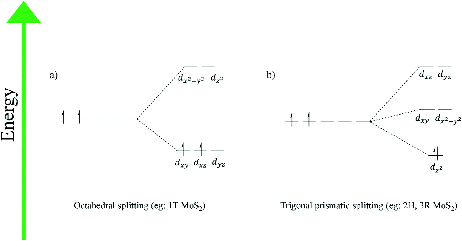 | ||
| Fig. 2 The splitting diagram and occupation of orbitals by d electrons in group VI TMDs in (a) octahedral coordination environments such as the 1T phase and (b) trigonal prismatic coordination environments such as the 2H and 3R phases. | ||
2H phase
The 2H polymorph belongs to the hexagonal crystal group. It involves the transition metal atom coordinated in a trigonal prismatic fashion. There are two repeating X–M–X units in its unit cell, with the atoms following an AbA BaB AbA pattern. 2H TMDs from Group VI of the periodic table are semiconducting, due to complete filling of the lowest energy dz2 orbital that arises from trigonal prismatic coordination (Fig. 2(b)).3R phase
The 3R polytype is similar to the 2H, in that it involves trigonal prismatic coordination of the transition metal. However, it differs in its stacking pattern. The unit cell involves 3 monolayers, stacked in an AbA BcB CaC AbA fashion. This polymorph belongs to the rhombohedral crystal group, and like the 2H phase, leads to semiconducting Group VI TMDs due to the trigonal prismatic coordination of the transition metal (Fig. 2(b)).15It should be noted that, in the case of monolayer TMDs, there are only two phases – 1T and 1H – as the stacking sequence is no longer a factor.
3. Bottom-up synthetic routes
In recent years, much progress has been made in the synthesis of TMDs through solution-phase bottom-up processes. The properties of the as-prepared TMDs vary widely with the use of different synthetic regimes, precursors, and stabilising ligands, giving rise to TMDs with a wide range of morphologies, phases and applications. In this section, the various established synthetic routes will be discussed, as well as the properties of the resulting TMD materials.3.1. Hydrothermal and solvothermal methods
Hydro/solvothermal methods refer to the synthesis of materials in closed vessels at high temperatures and pressures, carried out in water (hydrothermal) or other non-aqueous solvents (solvothermal).16,17 Hydro/solvothermal methods are commonly used in the synthesis of a variety of nanomaterials. They are also widely reported methods in the wet-chemical, bottom-up synthesis of TMD-based nanomaterials.The solvothermal and hydrothermal approaches to the synthesis of nanoscale TMDs date back to the years 1998 and 2000, respectively. Zhan et al. developed a solvothermal method for the production of nanocrystalline MoS2 using pyridine as the solvent, and MoO3 and elemental sulfur as the precursors.18 The use of this method resulted in the formation of thin platelets of semiconducting 2H MoS2, with average diameters of 100 nm. This was followed closely by Fan et al., who successfully synthesised nanocrystallites of MoS2 and MoSe2 for the first time via a hydrothermal method.19 Using Na2MoO4 as the Mo source and Na2S2O3/Na2SeSO3 as the sulfur/selenium sources, amorphous MoS2 and MoSe2 were formed, of average crystallite sizes 4 and 7 nm, respectively, which when annealed at 350 °C for 9 h resulted in the formation of the semiconducting 2H phase, in the case of both MoS2 and MoSe2. The synthesis of both involved the use of hydrazine as a reducing agent for the reduction of Mo(VI) to Mo(IV). These articles paved the way for the use of hydro/solvothermal methods in the bottom-up synthesis of ultrathin nanoscale TMDs.
Hydro/solvothermal synthesis of TMDs became very popular in the years that followed, producing nanostructures of various morphologies including nanosheets, nanotubes, nanorods, nanowires and nanoflowers.20–22
Wang et al. investigated the self-assembly behaviour of monolayer MoS2 synthesised via a simple solvothermal approach, using octylamine as the solvent and ethanol as an additive.23 In the absence of ethanol, MoS2 nanosheets were synthesised. However, in the presence of ethanol, hierarchical 3D tubular structures consisting of 2D nanosheets were formed (Fig. 3). The authors concluded that the formation of the tubular structure consisting of individual nanosheets, rather than a nanotube of restacked sheets, occurred due to a combination of factors. Firstly, ethanol in amine is a poor solvent, disrupting the interaction between nanosheets. Secondly, layered nanomaterials have a trend to form nanotubes under certain conditions. The octylamine capping ligands also prevent restacking of the sheets. The combination of these factors thus resulted in the formation of tubular arrangements of nanosheets, rather than single crystalline MoS2 nanotubes.
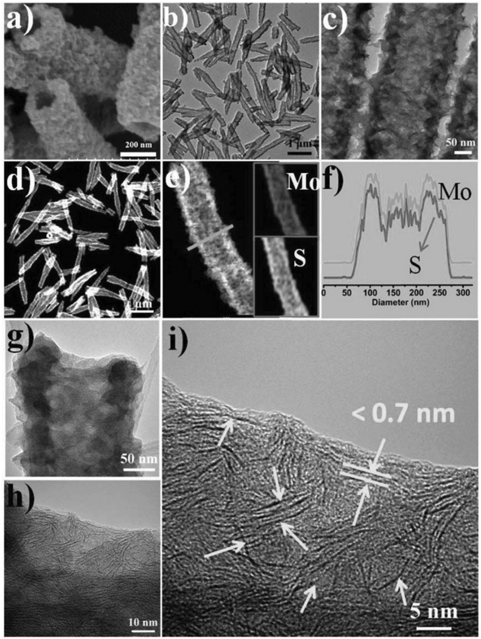 | ||
| Fig. 3 (a) SEM, (b and c) TEM, and (d and e) STEM images of the 3D architectures assembled from single-layered MoS2. The insets in (e) are EDX elemental maps, which clearly indicate that molybdenum and sulphur are uniformly distributed in the assembled architectures. (f) Corresponding EDS line scan profiles for Mo and S along the line in image (e). (g) TEM image of a single tube. (h) HRTEM image of the rim of the tube in (g). (i) Enlarged image in (g). The arrows indicate the separated layers with thickness below 0.7 nm. Reproduced from ref. 23. | ||
The authors also demonstrated that the diameter and length of the tubular structures could be tuned by changing the nature of alcohol present, using butanol as an example. It is also important to note that this synthesis is highly scalable, with 2 g of MoS2 hierarchical tubes being synthesised with ease, which is advantageous for potential commercial use.
3.2. Hot-injection methods
In the 1950s, LaMer and Dinegar proposed a set of conditions which are necessary to synthesise monodisperse colloidal solutions of nanoparticles, which involve a rapid nucleation step, followed by a slower step of controlled growth of nuclei to form larger particles.24 This motivated some groups of researchers to develop a new method of synthesising colloidal QDs, namely cadmium sulfide, selenide and telluride, which involved the rapid injection of organometallic precursors into vessels at high temperatures containing coordinating ligands and solvents.25 This method, termed ‘hot-injection’, has become commonplace in the synthesis of QDs, being used in the production of a wide variety of QDs, beyond just cadmium-based QDs.26,27In recent years, significant efforts have been made to apply the method of hot-injection to the synthesis of monodisperse TMDs. Small variations in the method, such as stabilising ligands, precursors, reaction time and temperature, are shown to produce TMDs of various phases, sizes and morphologies.
The as-produced QDs were ultra-small lateral size, few-layer nanosheets (Fig. 4). The authors found that an increase in the reaction temperature corresponded to an increase in the diameter of the WS2 QDs, due to the increase in the reaction rate.
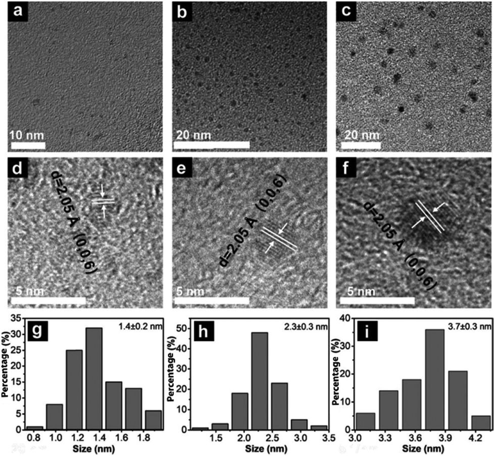 | ||
| Fig. 4 TEM images of WS2 QDs prepared at different reaction temperatures of (a) 255, (b) 275, and (c) 295 °C; (d–f) corresponding HRTEM images and (g–i) size distributions. Reproduced from ref. 32. | ||
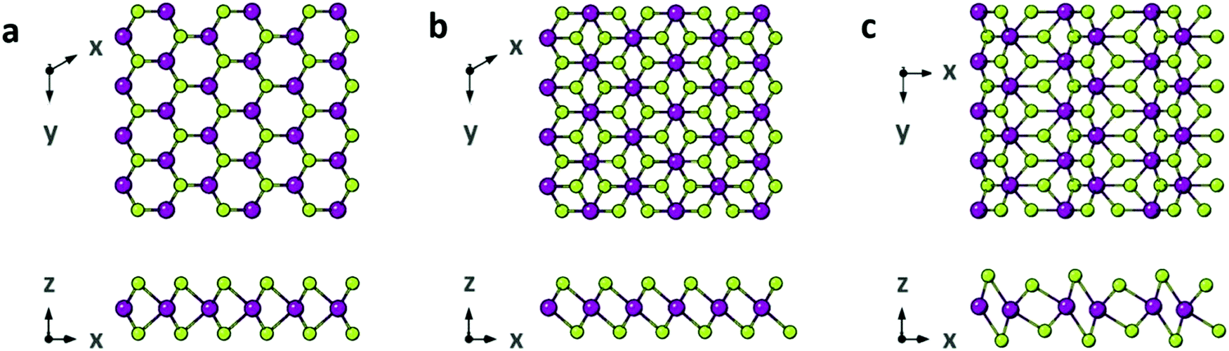 | ||
Fig. 5 Structural polymorphs of WSe2. (a) 2H WSe2 (space group P63/mmc). (b) 1T WSe2 (space group P![[3 with combining macron]](https://www.rsc.org/images/entities/char_0033_0304.gif) m1). (c) 1T′ WSe2 (space group P21/m). Reproduced from ref. 33. m1). (c) 1T′ WSe2 (space group P21/m). Reproduced from ref. 33. | ||
The resulting nanostructures exhibited a flower-like morphology, of average diameter 200 nm. The colloidal suspension of WSe2 nanoflowers in ethanol was observed to be stable under ambient conditions. The 1T′ nanoflowers were also fully convertible to the semiconducting 2H phase via annealing at 400 °C for 2 h, with no obvious changes in their size or morphology.
 | ||
| Fig. 6 TEM images of the 1H-MoS2@oleylamine flocculates give evidence for the presence of monolayer MoS2 nanosheets. The variation of the average nanosheet dimension from the reactions carried out at (a) 200 °C (average size of 4.78 ± 0.78 nm) and (b) 325 °C (average size of 11.29 ± 1.26 nm). The inserted images represent the SAED patterns, supporting the identification of the 1H crystallites. Reproduced from ref. 34. | ||
Jung et al. were able to produce size-controlled MoSe2 and WSe2 nanosheets using capping ligands with various binding energies to promote lateral growth of the nanosheets.35 Using Mo(CO)6/W(CO)6 and diphenyl diselenide (Ph2Se2) as precursors, they varied the capping ligand used in the synthesis from oleylamine to oleyl alcohol to oleic acid. It was found that the use of the amine resulted in small-lateral size, multi-layered sheets, the alcohol resulted in fewer layers and a larger lateral size, and the carboxylic acid resulted in the production of large lateral size (200–400 nm) monolayers (Fig. 7).
 | ||
| Fig. 7 Lateral size- and thickness-controlled synthesis of WSe2 nanosheets with the use of different capping ligands. (a) Visualization of single-layer WSe2 and its trigonal prism geometry with the ball-and-stick model. (b) Chemical equation for WSe2 nanosheets. (c) TEM images of WSe2 nanosheets synthesized with (i) oleylamine, (ii) oleyl alcohol, and (iii) oleic acid. (i′ and ii′) Magnified TEM images of the nanosheets, and (iii′) pseudocolor image of the single-layer nanosheets. (d) XRD patterns of WSe2 nanosheets synthesized with (i) oleylamine, (ii) oleyl alcohol, and (iii) oleic acid. (e) UV-vis absorption spectra of WSe2 nanosheets synthesized with (i) oleylamine (purple line), (ii) oleyl alcohol (orange line), and (iii) oleic acid (red line). Reproduced from ref. 35. | ||
Using DFT calculations, the researchers were able to show the significance of the binding energy of the capping ligand to the edge sites of MoSe2 and WSe2, and the effect this had on lateral size and thickness. It was demonstrated that the binding energy decreases on moving from the amine, to the alcohol, to the carboxylic acid. The strongly bound oleylamine stabilises the edge sites, favouring the formation of more layers and inhibiting lateral growth, whereas the weakly bound oleic acid does not offer much stabilisation to the edge sites of MoSe2 and WSe2, so lateral growth is favoured in this case. This insight into the factors controlling anisotropic growth in 2D materials may be a huge step forward for the solution-based bottom-up synthesis of these materials.
More recently, Zhou et al. successfully produced colloidal solutions of few-layer semiconducting 2H WS2, using an array of capping ligands – oleylamine (OAm), oleic acid (OA), trioctylphosphine oxide (TOPO), and squalane.36 Raman spectroscopy is commonly used for characterisation of Group VI TMDs such as MoS2 and WS2 to determine the number of monolayers present in the sample. The frequencies of the A1g out-of-plane chalcogen vibrational mode, and the E12g vibrational mode, which involves the in-plane displacement of transition metal and chalcogen atoms, are monitored. The Raman shift between these two phonon modes has a thickness dependence – it decreases with decreasing number of monolayers – allowing the thickness of a sample to be determined.37,38 The as-produced nanosheets were confirmed to have a thickness of 2 to 3 layers by AFM and Raman spectroscopy, and were reported to be of higher aspect ratio than those obtained by LPE combined with size-selective, post-processing steps.
It is clear that modification of the reaction conditions in the hot-injection approach – precursors, reaction temperatures and times, coordinating ligands, etc. – can result in the production of TMDs of a wide range of morphologies. The effects of changing these conditions need to be further understood in order for the hot-injection approach to be used widely in the synthesis of TMDs. In 2019, Geisenhoff et al. carried out a study on how ligands affect different properties of WSe2 nanocrystals, synthesised via hot-injection.39 The study involved the injection of a selenium precursor, Ph2Se2, into a mixture of tungsten hexacarbonyl [W(CO)6] and two ligands – OA and TOPO. It was found that, by altering the ratio of OA and the tungsten precursor, the reactivity of the reagents changed drastically – resulting in huge differences in the phases and morphologies of WSe2 products prepared under different conditions (Fig. 8).
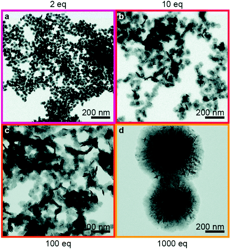 | ||
| Fig. 8 TEM images of WSe2 nanocrystals synthesised via injection of 1 mL of Ph2Se2 (0.04 M in TOPO or OA) into a solution of W(CO)6 (0.02 mmol) in OA/TOPO. The final reaction mixtures contained (a) 2, (b) 10, (c) 100 or (d) 1000 eq. OA/W. Reproduced from ref. 39. | ||
3.3. Other miscellaneous synthetic methods
Although the hydrothermal and hot-injection methods are the most widely reported in the solution-based bottom-up synthesis of TMDs, there are some other interesting colloidal synthetic methods available in the literature.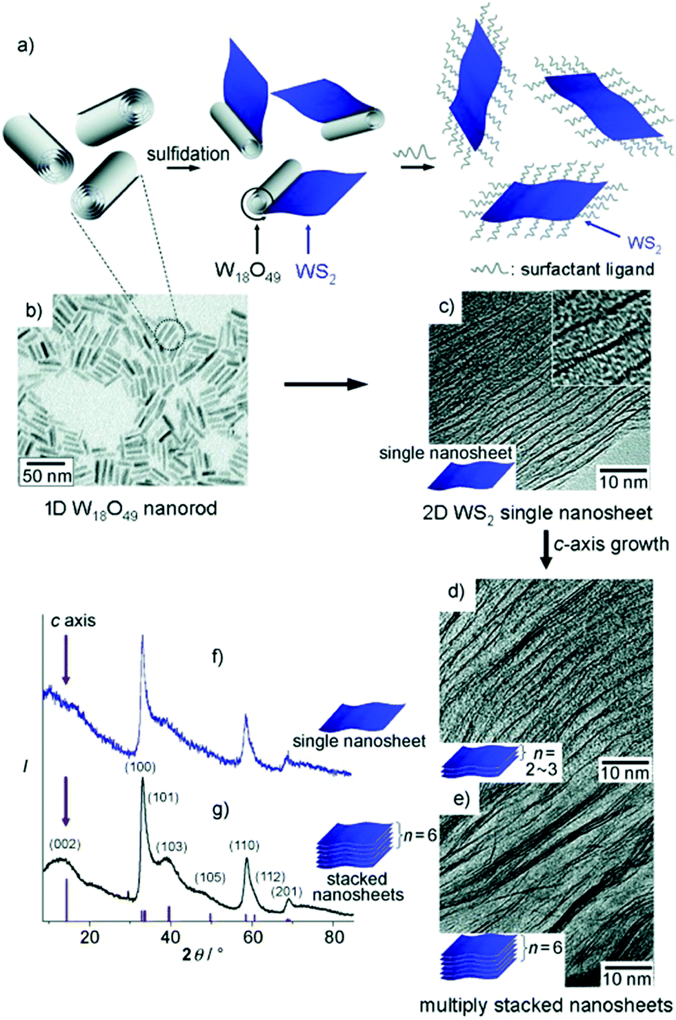 | ||
| Fig. 9 2D WS2 nanosheet crystal formation through rolling-out shape-transformation processes of 1D W18O49 nanorod precursors. (a) Schematic diagram for the synthesis of 2D WS2 nanosheet crystals. (b) TEM image of W18O49 nanorod precursors. (c–e) TEM images of 2D WS2 obtained with the reaction times of 10 min (c), 30 min (d), and 1 h (e) after the CS2 injection. (f) XRD analyses of the WS2 single (top) and stacked (bottom) nanosheet crystals (red lines: JCPDS reference card no. 08-0237). Reproduced from ref. 40. | ||
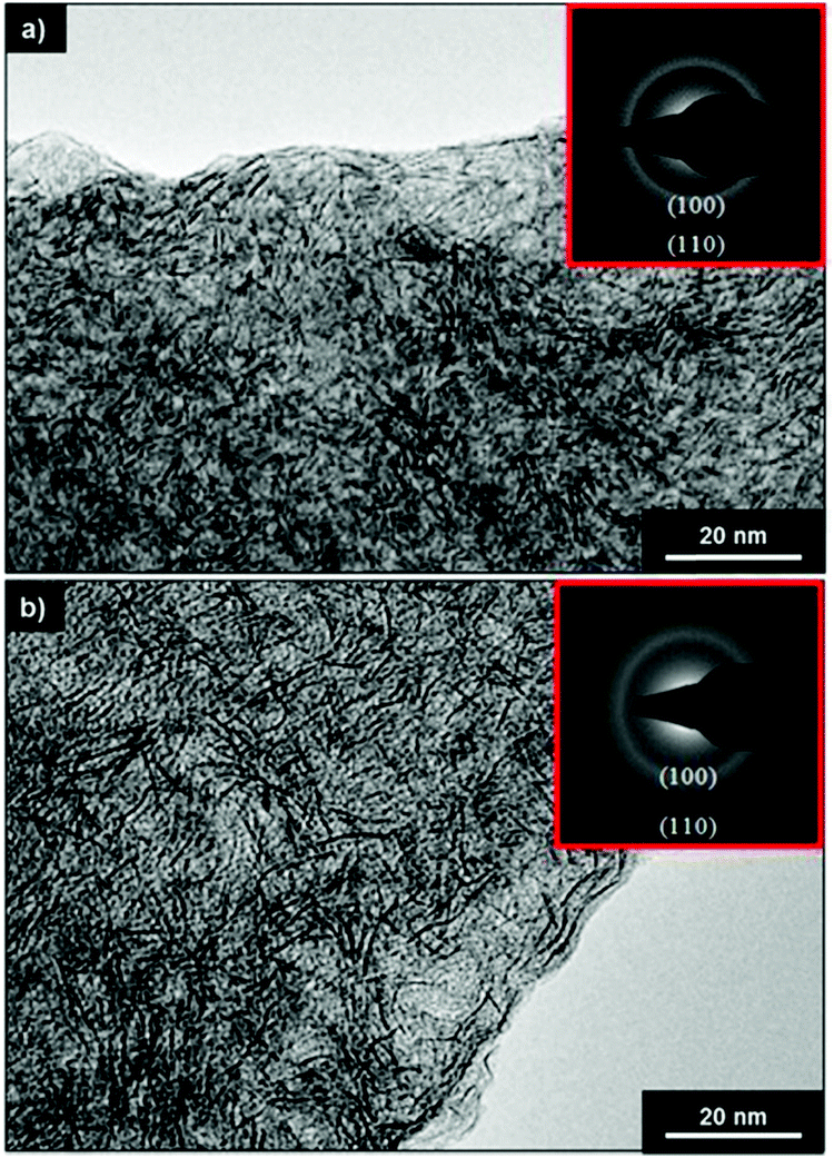
Mastria et al. followed a very similar approach in the production of WS2 thin films via hot-injection, followed by spin-coating, with some slight modifications.41 Oleylamine was used in place of hexadecylamine as the coordinating solvent, and elemental sulfur was used in place of CS2 for the sulfidation step. The oleylamine seemed to have provided superior colloidal stability compared to hexadecylamine as used by Seo et al., evidenced by the fact that no major restacking of the sheets was observed in the TEM images. The ultrathin nature of these oleylamine-stabilised WS2 nanosheets was shown by the low electron diffraction contrast under low magnification TEM imaging.
It is clear that the bottom-up synthesis of 2D TMDs is an exciting new field. The various techniques employed to make these materials are very versatile, and result in a wide variety of high quality TMDs, with varying sizes, phases, morphologies and other properties, with relative ease. The various synthetic techniques are summarised in Table 1.
| Method | TMD materials | Morphologies | Phases | Advantages | Disadvantages | Ref. |
|---|---|---|---|---|---|---|
| Hydrothermal | MoS2, MoSe2, WS2, WSe2 | Microrods, micro/nanoparticles, microspheres, nanosheets, nanoflowers, laterally confined monolayers (QDs) | Amorphous, 2H, 1T/1T′ | Simple, one-step process, aqueous phase synthesis | High temperatures and pressures required | 19–21 and 45–55 |
| Solvothermal | MoS2, WS2 | Platelets, nanosheets, 3D self-assembled tubes | 2H | Simple, one-step process | Requires solvents, may be hard to remove from the final product | 18, 22 and 23 |
| Hot injection | MoS2, MoSe2, WS2, WSe2 | Laterally confined monolayers (QDs), nanoflowers, monolayer and few-layer nanosheets | 1H, 2H, 1T′ | High level of controllability, monodisperse products | High temperatures, solvents may be hard to remove from the final product | 32–36, 39 and 56–58 |
| One-pot method | MoS2, WS2, RuS2 MoTe2, MoSe2, WSe2, RuSe2 QDs | Laterally confined monolayers (QDs) | 2H | Incredibly fast reaction time, uniform, monodisperse product, a wide variety of TMDs possible | — | 42 |
| Shape-transformation | WS2 ultrathin nanosheets | Ultrathin nanosheets, stacked nanosheets | 1T′, 2H | Highly monodisperse product | Multi-step process, requires high quality W18O49 nanorods as precursors | 40 and 41 |
| Calcination | WS2 | Nanosheets | 2H, 3R | Highly scalable, no use of surfactants required, allows for large quantities of nanomaterials to be produced | Multi-step process, very high temperatures required | 44 |
4. Applications
The benefit of the above-mentioned synthetic techniques is that they mainly give rise to phase-pure, monodisperse products, and that the phase, size and morphology can often be tuned by modification of the reaction conditions. TMDs have a wide variety of already-established applications, as well as potential applications, which are heavily dependent on their size, phase and morphology. In this section, some of the main applications of TMDs – biomedical, electronics and catalysis – will be discussed, and the importance of ‘bottom-up’ synthetic routes for achieving these applications will be highlighted.4.1. Biomedical applications
TMD nanostructures possess many unique and interesting properties which make them promising candidates for use in biomedical applications. Semiconducting 2D TMDs, such as MoS2 and WS2, have a direct bandgap, with monolayer MoS2 for example exhibiting strong photoluminescence at 627 and 677 nm, making them exciting candidates for use in biosensing and bioimaging.6,59 The exceptionally high surface-to-volume ratio of TMD nanosheets is also advantageous, as this is a key factor in choosing suitable nanomaterials for drug delivery.60 However, one drawback is that they typically exhibit poor stability in aqueous media, which can limit their potential use in biomedical applications.61 Surface functionalisation with suitable surfactants or biomolecules can overcome this problem. The benefit of bottom-up synthetic methods such as hydro/solvothermal and hot injection syntheses is that they involve the use of suitable surfactants or ligands that coordinate to and stabilise the nanomaterial. Therefore, wet-chemical bottom-up approaches to the synthesis of TMDs can allow for the material to be synthesised and stabilised/functionalised in the same process. Furthermore, these wet-chemical synthetic approaches often result in the production of more monodisperse, well-controlled TMD nanostructures than those obtained via top-down approaches, which is vital in ensuring consistency for biomedical applications.PEGylation is a functionalisation method commonly used to make nanomaterials more suitable for biomedical applications. It involves the attachment of polyethylene glycol (PEG) molecules to other entities.62 PEGylated nanomaterials have the advantage of better water solubility, reduced immunogenicity when introduced into the body, and prolonged blood circulation time.63
Kumar et al. developed PEGylated MoS2 microspheres via a hydrothermal method for use as potential anti-cancer agents.43 Using ammonium heptamolybdate tetrahydrate and thiourea as precursors, and the addition of PEG as a stabilising ligand, they successfully produced 2–4 μm microspheres, consisting of bundles of ultrathin sheets of PEGylated 2H MoS2. The authors found, through altering the concentration of PEG used in the reaction, that PEG played a vital role in the self-assembly of the PEGylated MoS2 to form the hierarchical micro-spherical structure. These PEGylated MoS2 microstructures were shown to have excellent cytotoxicity towards cells from the MCF-7 breast cancer cell line, due to PEGylation aiding in the cellular uptake of MoS2. It is worth nothing that MoS2 nanostructures have been previously shown to exhibit low toxicity towards normal cells. These ‘bottom-up’ synthesised MoS2 nanostructures, thus have the capability to act simultaneously as both imaging/sensing and anti-cancer agents.
One particularly exciting potential application of TMD nanostructures is as agents for photodynamic (PDT) and photothermal therapy (PTT).64,65 PDT is an anti-cancer treatment, and involves the use of light and photosensitive species. When the photosensitive compound is in the body, under conditions of no light irradiation, it is non-toxic. However, when the photosensitive compound is exposed to light of correct wavelength, it is activated, producing reactive oxygen species (ROS). ROS are toxic to cells, therefore inducing cell death in the targeted area.66 PTT is a type of PDT which does not require the generation of ROS. Instead, light irradiation (usually infrared) of the photosensitive species triggers the release of heat, killing the targeted cells.
Wang et al. produced MoSe2 nanoflowers via a hot injection approach for potential use as PTT/PDT agents, using sodium molybdate and selenium powder as transition metal and chalcogen sources, respectively.56 The resulting semiconducting 2H MoSe2 nanoflowers, which consisted of 150 nm diameter bundles of sheets, each 3–4 layers thick, displayed a strong absorbance in the NIR region, at 808 nm. These MoSe2 nanoflowers showed high photothermal stability, and demonstrated superior photothermal conversion efficiency (61.8%) compared to similar previously synthesised MoSe2-based PTT agents, such as PVP-coated MoSe2 nanosheets (57.9%) and MoSe2@PDA nanocomposites (44.5%).67,68 The high photothermal conversion efficiency of these MoSe2 nanoflowers can be attributed to their branched, nanoflower-like morphology, which is readily achievable only through solution-based bottom-up synthetic strategies such as hydro/solvothermal and hot-injection syntheses. Furthermore, the MoSe2 nanoflowers were found to be effective in producing reactive oxygen species, necessary for PDT. These nanoflowers were subsequently PEGylated for further experiments to increase biocompatibility, and these PEG–MoSe2 nanohybrids were loaded with an anticancer drug, Doxorubicin (Dox), to investigate their loading capacity and potential for controlled drug release (Fig. 10). The nanoflowers were found to have a high drug loading capacity of Dox (12.6 ± 2.5 wt%), with inhibited drug release at pH 7.4, and enhanced release of Dox under acidic conditions of pH 5, which is significant as tumour sites are weakly acidic, displaying pH values of around 4–5. Therefore, the authors, through a simple bottom-up synthetic approach, produced MoSe2-based nanostructures with strong potential for use as PTT/PDT/chemotherapy agents.
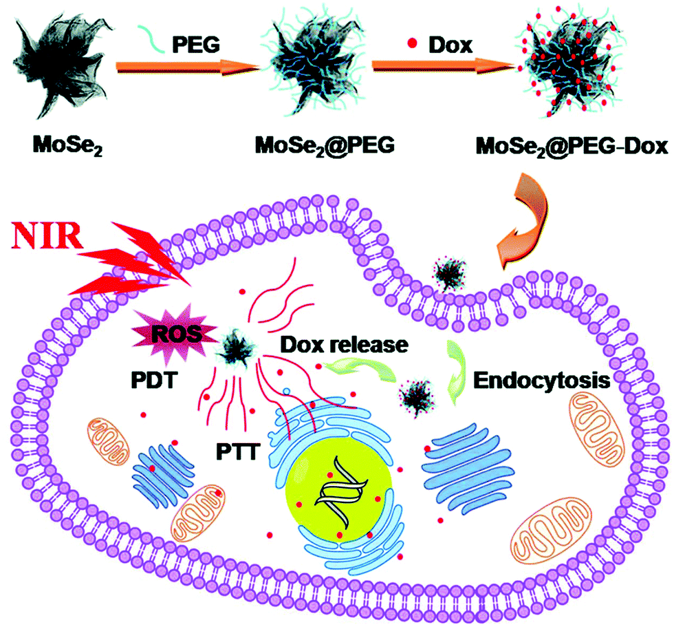 | ||
| Fig. 10 Schematic representation of the preparation and therapeutic action of MoSe2@PEG–Dox nanocomposites. Reproduced from ref. 56. | ||
In addition to potential anti-cancer applications, some recent studies have also focused on the potential of TMD nanomaterials as antibacterial agents. Masimukku et al. synthesised <1 μm wide, single-to-few layer WS2 nanoflowers via a hydrothermal method, using sodium tungsten dihydrate and thiocarbamide as tungsten and sulfur sources, respectively (Fig. 11).46
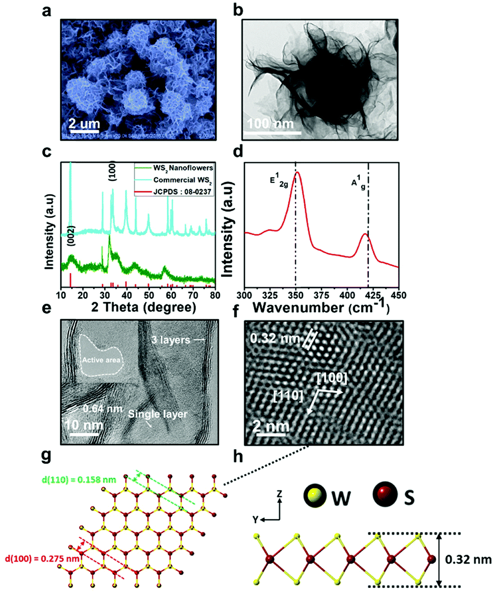 | ||
| Fig. 11 (a) FESEM image of the WS2 NFs showing the size in the range of 0.5 μm. (b) Low-magnitude TEM image showing an individual nanoflower of WS2. The HRTEM image showing the WS2 NFs with a great number of single layer and few layers. (c) The XRD patterns of commercial WS2 (upper pattern) and WS2 NFs (lower pattern). (d) Raman spectra of as-synthesised WS2 NFs. (e) The abundant single- and few-layered WS2 NFs with a lattice spacing of ∼0.64 nm; the greatly dispersed nanopetals offer rich active edge sites. (f) The HRTEM image of single-layer WS2. (g) and (h) The atomic structure of single layer of WS2. Reproduced from ref. 46. | ||
Through piezoresponse force microscopy (PFM), the resultant metallic 1T WS2 nanoflowers were shown to have a piezoelectric response. This piezoresponse was examined further to see if the WS2 nanoflowers exhibited piezo-degradation ability towards Rhodamine-B (Rh-B) dye. WS2 nanoflowers were dispersed in a solution of Rh-B and subjected to ultrasonication in the dark for 200 s, and were found to exhibit 99% degradation of Rh-B. As a control, WS2 nanoflowers were dispersed in Rh-B for 200 s in the dark and in the absence of ultrasonication, and negligible amounts of Rh-B were degraded, which is evidence that the degradation occurs due to mechanical strain on the WS2 nanoflowers when subjected to ultrasonication. The degradation potential of WS2 nanoflowers was also tested on E. coli K12 cells. After ultrasonication for 60 min, >99.99% of E. coli K12 cells were observed to have been destroyed. This first report on the production of singlet oxygen species and hydroxyl free radicals by WS2 nanoflowers under the conditions of ultrasonication and no light irradiation is a very significant result, and could pave the way for further application of TMDs in catalysis and as antibacterial agents.
Research into photocatalytic activity of TMDs is more common than non-light-driven catalysis, and may also be beneficial for use in antibacterial applications. Askari et al. produced porous hexagonal-phase MoS2 nanoparticles via a hydrothermal approach using sodium molybdate and thioacetamide as metal and chalcogen precursors, respectively.47 As an initial test of the nanomaterial's photocatalytic activity, different amounts of solid MoS2 nanoparticles were added to methylene blue (MB) solution and subjected to light irradiation under a 100 W tungsten bulb. The photocatalytic activity was highest at a MoS2 concentration of 15 mg L−1. Once the photocatalytic capability via generation of reactive oxygen species of the porous MoS2 nanoparticles was confirmed, the authors tested them for potential antibacterial applications, using both Gram positive (Staphylococcus aureus) and negative (E. coli DH5α) bacterial samples (Fig. 12). The porous MoS2 was found to be more effective as an antibacterial agent than both raw MoS2 powder and MoS2 nanosheets.69
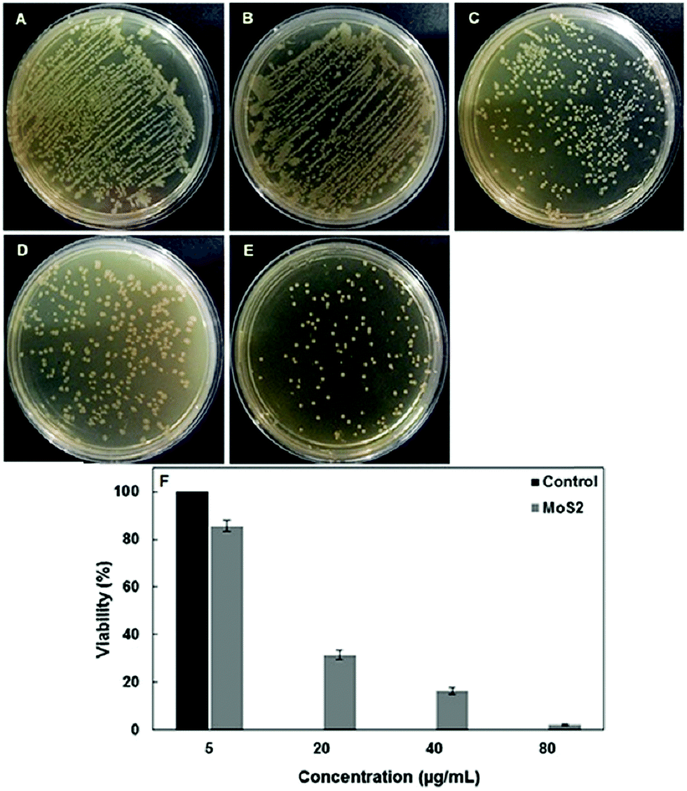 | ||
Fig. 12 Viability of E. coli cells in the absence of porous MoS2 (A) and after 2![[thin space (1/6-em)]](https://www.rsc.org/images/entities/char_2009.gif) h exposure to different concentrations of porous MoS2 (5μg mL−1 (B), 20 μg mL−1 (C), 40 μg mL−1 (D) and 80 μg mL−1 (E)). (F) Cell viability is plotted as the percentage of colony-forming units of bacterial samples exposed to different concentrations of MoS2 (gray bars) relative to the control (in the absence of porous MoS2; black bar). Reproduced from ref. 47. h exposure to different concentrations of porous MoS2 (5μg mL−1 (B), 20 μg mL−1 (C), 40 μg mL−1 (D) and 80 μg mL−1 (E)). (F) Cell viability is plotted as the percentage of colony-forming units of bacterial samples exposed to different concentrations of MoS2 (gray bars) relative to the control (in the absence of porous MoS2; black bar). Reproduced from ref. 47. | ||
It is clear that TMDs show huge potential for use in a variety of different biomedical applications. The monodispersity of bottom-up synthesised TMDs is hugely advantageous for use in the biomedical realm. However, more studies on the biocompatibility and in vivo toxicity of TMD nanostructures synthesised via bottom-up approaches are required to assist in the progression of this field.
4.2. Electrocatalysis and photocatalysis
As detailed above, many examples of the biomedical applications of 2D TMDs, in particular their antibacterial activity, are catalytic by nature. 2D TMDs have been recently explored as potential photocatalysts, in particular for use in the hydrogen evolution reaction (HER). A key factor in the reaction kinetics of the HER is the hydrogen adsorption Gibbs free energy (ΔGH).70 In general, the closer the value of ΔGH is to zero, the higher the catalytic activity. Using density functional theory, Hinnemann et al. demonstrated the potential of MoS2 as a catalyst for HER, displaying a ΔGH value of 0.08 eV – very close to the ideal value of 0 eV.71 Nano-scale TMDs, in particular MoS2, have been also explored as alternatives to platinum for HER due to their low cost and high earth abundance.72 The catalytic activity of nanoscale TMDs can vary widely with phase, morphology, and defects.73 For example, the metallic phases of TMDs such as MoS2 and WS2 (1T and 1T′ phases) typically exhibit higher catalytic activity in HER than their semiconducting, 2H-phase counterparts, due to the catalytic active sites being distributed on both the basal planes and the edge sites in the metallic TMD phases.74 Thus, the preparation of TMDs for catalytic applications through bottom-up approaches can be advantageous for many reasons.Solution-phase bottom-up synthesis allows for often more catalytically active, metastable phases (such as 1T and 1T′ in the case of group VI diselenides and disulfides) to be easily accessed.75 Production of TMDs exhibiting these phases via traditional methods such as Li intercalation and chemical exfoliation presents problems such as in non-phase pure samples, as well as metallic TMD samples often reverting back to the thermodynamically stable 2H phase after some time.76 However, through solution-based synthesis, involving stabilisation with appropriate ligands or surfactants, long-term stable, phase-pure 1T and 1T′ phases are readily accessible.
Wang et al. developed a hydrothermal approach for the synthesis of metallic MoS2 nanopetals for use as catalysts for HER.48 1T and 1T′ phase TMDs typically exhibit higher catalytic activity because both the basal plane and edge sites are active. However, the edge sites have higher activity for HER than the basal planes, so 1T/1T′ phase TMDs with abundant edge sites would be advantageous for HER. The petal-like MoS2 nanostructures, of an average thickness of 5 layers and a lateral size of 75 nm, result in abundant exposed active edge sites, in turn resulting in high electrochemical activity for HER. The bottom-up synthesised metallic MoS2 nanopetals showed superior HER performance compared to bulk, exfoliated and semiconducting MoS2, with an exceptionally low overpotential of 210 mV at a current density of 10 mA cm−2, and a small Tafel slope of 44 mV per decade, approaching ideal, platinum-like behaviour (Fig. 13).
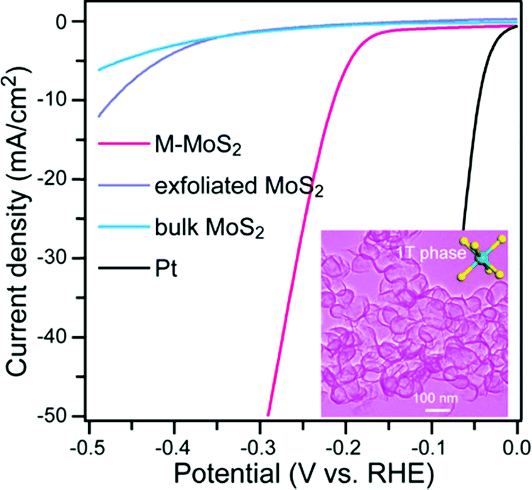 | ||
| Fig. 13 Polarization curves after iR correction for M-MoS2 in comparison with bulk MoS2, exfoliated MoS2 and Pt/C. Inset: TEM image of M-MoS2 nanopetals. Reproduced from ref. 48. | ||
In addition, colloidal synthesis allows for TMDs to be grown directly on a given substrate or electrode, which is highly desirable for electrocatalytic testing. Sokolikova et al. demonstrated this by growing 1T′ WSe2 nanoflowers directly on carbon paper, carbon foil and gold foil via a hot injection approach.33 Another advantage of colloidal synthesis is the potential for controlled introduction of defects into the nanostructures, which can result in improved catalytic activity.77
Xie et al. produced defect-rich, hexagonal phase MoS2 nanosheets for application as HER catalysts via a hydrothermal approach.49 Thiourea was employed as the sulfur source, with the additional role of reducing Mo(VI) to Mo(IV), as well defect engineering of the resultant MoS2 nanosheets. By varying the concentration of thiourea used in the hydrothermal reaction, the authors discovered that the number of defects could be controlled, thus controlling the efficacy of the MoS2 nanosheets for use as a catalyst in HER. The excess thiourea acts as a stabilising agent for the MoS2 nanosheets, partially hindering the growth, resulting in a defect-rich structure (Fig. 14). The introduction of defects significantly improves the catalytic activity as, in hexagonal/2H-MoS2, the basal planes are inert. The defects cause cracks in the basal planes of the nanosheets, forming more edge sites, which are catalytically active. It is also worth noting that this synthesis is done on the gram-scale, and is highly scalable, which lends itself to potential industrial applications.
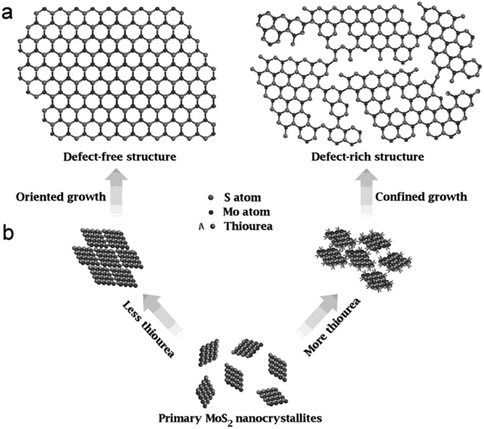 | ||
| Fig. 14 (a) Structural models of defect-free and defect-rich structures. (b) As-designed synthetic pathways to obtain the above two structures. Reproduced from ref. 49. | ||
The photocatalytic properties of TMDs have been exploited for many applications other than HER. Removal of contaminants of natural water supplies is a huge challenge and an exciting area of research. 2D materials such as hexagonal boron nitride and TMDs are being used for this purpose, often in the form of membranes for nanofiltration.78 One such harmful contaminant is hexavalent chromium (Cr(VI)).79 Cr(VI) is a known carcinogen, mutagen, as well as a toxic element to plants, animals and microbes.80 However, the use of nanofiltration for removal of Cr(VI) from water supplies may have limited efficacy, as the technique suffers from drawbacks such as membrane fouling.81 An alternative route for the removal of Cr(VI) from water is the reduction of Cr(VI) to Cr(III), which is significantly less toxic. Chu et al. produced 2H MoSe2 nanosheets via a hydrothermal route for examination of their photocatalytic activity for the reduction of Cr(VI) to Cr(III) under different pH conditions.50 An advantage of MoSe2 over other photocatalysts is that it exhibits photocatalytic activity over the UV, visible and IR regions, whereas many other photocatalysts only operate in the UV and visible regions, which account for only 46% of the solar energy reaching earth. The MoSe2 prepared at a pH of 2 had higher absorption and a larger specific area, resulting in the best photocatalytic activity. After 3 h, MoSe2 resulted in 99%, 91% and 98% reduction of Cr(VI) to Cr(III) under UV, visible and IR light irradiation, respectively. The use of “bottom-up” synthetic methods in this case allowed for the production of MoSe2 with ultrahigh specific surface area, which aided in the exceptional performance of the photocatalyst.
4.3. Electronics and optoelectronics
2D materials have been the subject of much research interest for potential electronic applications in recent years. For some time, graphene was the main focus, due to its high electron mobility, flexibility, transparency, tensile strength and thermal conductivity.82 However, the major disadvantage of graphene is that it lacks an electronic bandgap, thus limiting its potential application as a material for use in transistors.83 2D TMDs also exhibit many of the advantageous properties of graphene, with the additional benefit of having a non-zero bandgap, as well as exhibiting phase-dependent conductivity behaviour, ranging from metallic (e.g. 1T MoS2) to semiconducting (e.g. 2H MoS2).84A significant drawback of solution-phase exfoliated 2D materials is their polydispersity.85 For electronic device applications, uniform sheets of material are required, to ensure consistency across devices if produced on a large scale.86,87 This can be achieved by synthetic methods such as hydro/solvothermal and hot-injection approaches; however the photophysics of colloidal TMDs are not well studied. Schiettecatte et al. produced ultrathin, 2–4-layer MoS2 nanosheets via hot-injection.58 Using transient absorption spectroscopy, a detailed study was carried out on the charge carrier dynamics in colloidal MoS2. The authors found that the carrier dynamics in colloidal MoS2 followed a very similar behaviour to that of CVD-grown MoS2, suggesting that colloidal synthesis of MoS2 yields nanosheets of comparable quality to those grown by state-of-the-art CVD.
Similarly, Zhou et al. produced ultrathin 2H WS2via a hot-injection approach to gain insight into the photophysics of the nanosheets necessary to exploit their potential application in optoelectronics.36 They too found that the colloidal WS2 nanosheets exhibited a very similar photophysical behaviour to that of CVD-grown WS2. This demonstrates the huge potential of bottom-up synthesis of TMDs, as it is possible to produce CVD-quality nanosheets at a fraction of the cost and under much less extreme conditions.
One of the advantages of using colloidal suspensions of TMDs in electronics is that they can be spin-coated or printed onto suitable substrates, to easily and inexpensively prepare TMD thin films.88,89 As mentioned previously, Mastria et al. developed a shape-transformation approach involving hot-injection, to produce ultrathin, oleylamine-stabilised, colloidal WS2 nanosheets for the production of solution processable, conducting thin films for device integration.41 Treatment of the thin films after deposition with diluted superacid resulted in partial removal of the oleylamine ligands, helping the nanosheets to orient parallel to the substrate, which is critical for increasing the planar conductivity of the WS2 thin-film. The 40–140 μm thick films, before post-deposition treatment, were shown to be highly insulating, due to the presence of oleylamine ligands. However, after treatment and partial removal of oleylamine, the sheet resistivity was dramatically reduced, displaying conductivity values comparable to that of pristine few-layer to monolayer semiconducting WS2 nanosheets obtained by mechanical exfoliation.90
Son et al. developed a gram-scale hot-injection synthesis for the production of uniform, monodisperse, 2-layer-thick MoS2.57 Using HRTEM and STEM, the authors were able to show that the colloidal MoS2 was thinner and significantly more monodisperse than exfoliated MoS2. A resistive random-access memory (RRAM) device was prepared using the colloidal MoS2via a spray coating deposition technique on aluminium electrodes. A similar device using exfoliated MoS2 was also fabricated as a control. The synthetic MoS2 RRAM exhibited superior uniform device performance, displaying an on/off ratio 10000 times higher than that of the exfoliated MoS2-based RRAM device, due in part to the uniformity of the colloidal MoS2 nanosheets. By conducting strain analysis of colloidal MoS2-based RREM using a flexible substrate, the authors demonstrated the exciting potential of colloidal MoS2 for use in wearable, flexible electronics (Fig. 15).
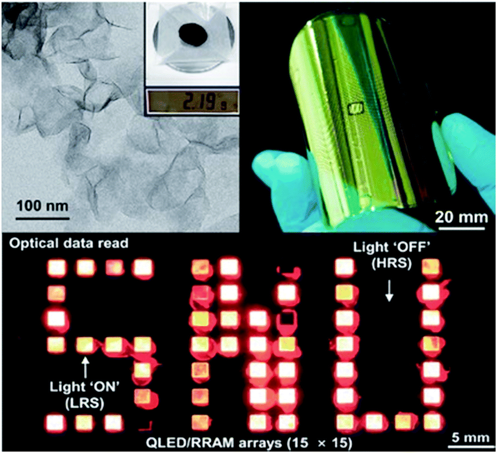 | ||
| Fig. 15 (top-left) TEM image of 2-layer thick MoS2 nanosheets. The inset shows that the synthesis occurs on a gram scale. (top-right) Flexible RREM device made from MoS2 nanosheets via a spray deposition technique (bottom) QLED-RRAM array based on MoS2 nanosheets and CdSe QDs. Reproduced from ref. 57. | ||
Another emerging application of TMD nanostructures is as field emitters. Field emission involves the emission of electrons from a material induced by an electric field.91 Generally, metallic and semiconducting nanomaterials are good natural field emitters, particularly 1D and 2D nanostructures, which can cause local electric field enhancement due to their high aspect ratio.92 However, the field emission effects from more exotic morphologies of TMDs such as nanoflowers are not well understood. Giubileo et al. produced MoS2via a hydrothermal approach to investigate their field emission characteristics.52 The 2H phase, 100–200 nm diameter nanoflowers were probed using tungsten tips as electrodes inside the SEM chamber. The use of small tips as electrodes allowed the field emission to be probed locally, at areas as small as 1 μm2, showing that the protruding sheets of the nanoflowers acted as strong field emitters, with electronic emission occurring at electric fields as low as 12 V μm−1. These field emitting MoS2 nanoflowers could find application in areas such as cathode materials for electron microscopy and optical displays, to name a few.93–95 It is important to mention that this unique field emission behaviour is characteristic of the flower-like morphology obtained via hydrothermal synthesis, highlighting the advantages of bottom-up synthesis and interesting applications which can arise from these synthetic approaches.
An emerging potential application for 2D TMD-based nanomaterials is valleytronics, which involves the use of the electron wave quantum number in a crystalline material to encode data by controlling the photon angular momentum (circular polarisation state) via circular polarised light.96 This area is rapidly developing and so far is mostly focused on the use of atomic layered transition metal dichalcogenides (TMDs), such as MoS2.97 Hexagonal TMDs are of particular interest for valleytronics applications as they lack inversion symmetry, which allows for different circular dichroism (CD) behaviour in each of the valleys.98 The induction of chirality in 2D materials may be of particular interest for valleytronics applications, due to the strong interaction with circularly polarized light. This has recently been achieved in MoS2 by liquid-phase exfoliation in the presence of chiral ligands such as cysteine and penicillamine.99 The functionalized MoS2 showed multiple intense CD peaks, far beyond the onset of CD signals due to the ligands alone (Fig. 16). The benefit of bottom-up synthetic approaches is that they allow for the production of high quality, size-controlled samples, with the ability to functionalise the nanomaterial in situ. Thus, the development of these synthetic techniques has the potential to mass produce monolayer-rich dispersions of colloidal, chiral TMDs for use in valleytronics applications.
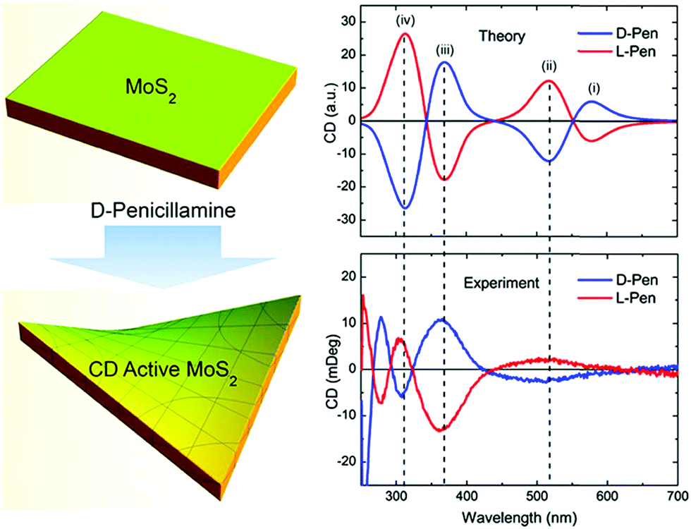 | ||
| Fig. 16 (left) Schematic showing functionalisation of MoS2 with penicillamine and subsequent induction of chirality. (right) Theoretical (top) and experimental (bottom) CD spectra for L- and D-penicillamine functionalised MoS2. Reproduced from ref. 99. | ||
4.4. Sensing applications
Gas sensors are commonplace in both industrial and residential settings, and are vital to protect people from potential exposure to harmful, noxious gases, as well as having application in medical diagnostics.100 In recent years however, there has been significant demand for, and interest in, wearable electronics, and integration of gas sensors into the likes of smartphones and smart watches, with the aim of providing the user with real-time information about their environment, as well as to monitor their health and wellbeing.101,102 2D materials have been explored for small scale gas sensors for device integration as their large surface to volume ratio means there are abundant sites available for target gases to bind to, allowing for exceptional sensitivity.103 Furthermore, TMDs in particular are regarded as good candidates for gas sensing technologies, as they can operate at room temperature due to their high electron mobility, which significantly reduces power consumption.104Solution-based bottom-up approaches for the synthesis of TMDs for gas sensing technologies are preferable, as they allow for a high yield of the product, at low-cost and with good controllability over particle size and morphology. Thang et al. synthesised a MoS2-based gas sensor, fabricated by drop-casting MoS2 nanoflowers – obtained via a hydrothermal approach – on platinum electrodes.53 The sensor, which operated at room temperature, showed excellent selectivity to sensing NO2 gas in the presence of other interfering gases and an exceptionally low detection limit of 84 parts per billion, and the sensing properties did not vary with environmental humidity. It is also worth noting that the authors attributed the exceptional sensing capabilities of this MoS2-based NO2 sensor to the thin petals of the flower-like morphology obtained via hydrothermal synthesis.
TMD-based nanomaterials are also good candidates for solution-phase chemical sensing for a variety of applications, from environmental (e.g. heavy metal ion detection) to medical diagnostics.105,106 Both monolayer TMD nanosheets and TMD QDs are luminescent in the visible region, making them viable candidates for use in fluorescent sensors. Sun et al. synthesised MoS2 QDs via a hydrothermal approach for the detection of rutin, a glycoside found in fruits and grains which has been shown to have medicinal properties.54,107 The authors found that on contact of rutin with MoS2 QDs, the fluorescence intensity decreased, and this decrease became more pronounced on addition of higher concentrations of rutin (Fig. 17). The quenching mechanism was determined to be due to the inner filter effect.
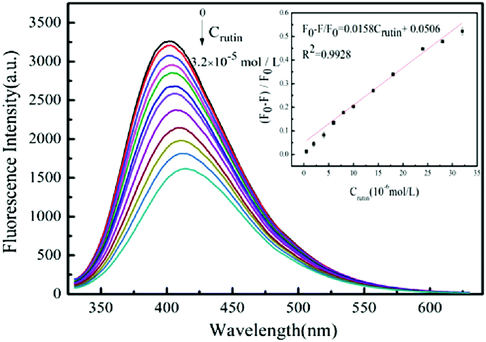 | ||
| Fig. 17 Fluorescence spectra of MoS2 quantum dots (QDs) with various concentrations of rutin. The inset shows the linear relationship between F0 − F/F0 and rutin concentration. Reproduced from ref. 54. | ||
The MoS2 QD fluorescent sensor was found to be comparable to other, more complicated and expensive detection techniques such as high-performance liquid chromatography (HPLC) and microsequential injection analysis (MIA), with a lower detection limit of 0.35 μM. The sensor also showed high selectivity towards detection of rutin in the presence of metal ions and common pharmaceutical additives.
4.5. Energy harvesting and storage
As previously mentioned, as the demand for wearable electronics has soared in recent years, so too has the demand for energy harvesting materials for integration into these devices as a green, sustainable energy source. Harvesting energy created by the body through movement and heat and converting it to electricity is an area of significant interest.108 One such energy harvesting device is the thermoelectric generator, which generates electricity from a temperature gradient across a material. For a thermoelectric generator to be highly efficient, the material needs to have a high Seebeck coefficient, high electrical conductivity, and low thermal conductivity.109 Xie et al. developed a thermoelectric nanogenerator based on a 2H-MoS2/graphene hybrid material via a hydrothermal approach.110 The reason for choosing a hybrid material is because both graphene and MoS2 have advantages and drawbacks for use in a thermoelectric generator. MoS2 has a high Seebeck coefficient and low thermal conductivity; however its large bandgap results in low electrical conductivity.111 Graphene, on the other hand, is a zero-bandgap semimetal, so has high electrical conductivity, but suffers from high thermal conductivity and a low Seebeck coefficient. The resulting MoS2/graphene nanocomposite was found to have improved electrical conductivity compared to pristine MoS2, while still maintaining low thermal conductivity and a high Seebeck coefficient. A flexible thermoelectric generator was produced using this MoS2/graphene nanocomposite, and was shown to generate an output voltage 2 times higher than that generated by pure MoS2 and 8 times higher than that generated by pure graphene thermoelectric nanogenerators.Another promising application of TMD nanomaterials is their use as anode materials in lithium ion batteries. A huge advantage of bottom-up synthesis of TMDs is that it can offer great controllability over properties such as size, phase and morphology, which can be crucial for energy storage applications. Lu et al. prepared MoS2 nanoflowers via a hydrothermal approach, using the reaction temperature to tune the interlayer distance between the constituent MoS2 nanosheets.51 It was shown that at higher temperatures, the interlayer spacing between the MoS2 nanosheets was decreased, as evidenced by the shift to higher angles of the (002) peak in the XRD patterns of different MoS2 samples. The increased reaction temperature also resulted in the formation of thinner nanosheets and nanoflowers with increased surface area, which is desirable for optimised lithium ion insertion–extraction. The sample with the best electrochemical activity was synthesised at 200 °C, exhibiting superior rate capability and lithium storage capacity. At this temperature, the MoS2 nanoflowers were found to have an optimal interlayer distance (0.65 nm) as well as improved crystallinity, the presence of some defects, and an enhanced specific surface area, which are also vital for optimising the electrochemical performance.
4.6. Photonics applications
Saturable absorption is a phenomenon by which the absorption of light by a given material decreases with increasing light intensity. The saturable absorption properties of 2D materials have been extensively studied in recent years for Q-switching and mode-locking in ultrafast compact pulsed lasers.112 Few layer to monolayer TMDs such as MoS2 and WS2 are particularly useful for these applications as their direct bandgap falls in the visible range, whereas many other 2D materials used for these purposes are limited to operation in the infrared region.113,114 Few-layer to monolayer nanosheets are often studied for their saturable absorption properties; however more exotic morphologies such as nanoflowers obtained through bottom-up synthesis are neglected. Sun et al. investigated the saturable absorption properties of MoS2 nanosheets and, for the first time, nanoflowers synthesised via a hydrothermal approach.55 The colloidal MoS2 samples were then mixed with 1% polymethyl methacrylate (PMMA) in toluene solution and spin-coated onto a quartz substrate to fabricate the saturable absorber (SA) for insertion into the Yb:GAB laser cavity (Fig. 18).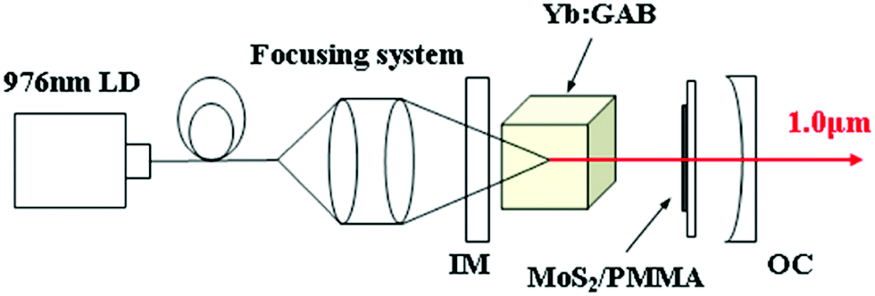 | ||
| Fig. 18 Schematic experimental setup of the Q-switched Yb3+:GAB solid-state laser. Reproduced from ref. 55. | ||
The nanosheets had Q-switching properties comparable to those of other MoS2 SAs obtained via exfoliation, displaying shortest pulse widths of 281 and 216 ns for single and dual wavelength laser sources, respectively. The nanoflowers, however, displayed superior optical switching behaviour compared to the nanosheets, with pulse widths of 209 and 198 ns for single and dual wavelengths. The authors attributed this enhanced non-linear optical behaviour to the unique morphology of the nanoflowers obtained via hydrothermal synthesis. Thus, further development and research in the field of bottom-up synthesis of TMDs may open the door for large-scale application of TMDs in lasers, due to its cost efficiency, scalability, and high-quality products.
Group VI monolayer 2H TMDs such as MoS2 and WS2 display photoluminescence due to the indirect to direct bandgap transition on being reduced from the bulk to the monolayer. This phenomenon has led to a multitude of potential applications of monolayer TMDs in photonics and optoelectronics. One of the limitations of the use of monolayer TMDs in photonics applications is the quantum yield (QY). The QYs of many pristine monolayer TMDs are often very low (<1%), likely due to non-radiative electron–hole recombination mediated by defects.115,116 However, chemical doping is an effective method of passivation of these non-radiative decay pathways, resulting in significant enhancement of the QY of monolayer TMDs. Mouri et al. discovered that doping with 2,3,5,6-tetrafluoro-7,7,8,8-tetracyanoquinodimethane (F4TCNQ) and 7,7,8,8-tetracyanoquinodimethane (TCNQ), both p-type dopants, dramatically increased the photoluminescence (PL) quantum yield of mechanically exfoliated monolayer MoS2.117 Amani et al. reported similar findings upon the treatment of monolayer MoS2 with bis(trifluoromethane)sulfonimide (TFSI), an organic superacid, resulting in a PLQY enhancement from 0.6% to >95%.118 Solution-based “bottom-up” synthetic methods allow for the doping of TMDs in situ, which may pave the way for the production of size-controlled, high PLQY monolayer TMDs in a one-pot process. Highly luminescent monolayer TMDs synthesised via bottom-up approaches may find application in areas of photonics such as highly efficient LEDs, as single photon emitters for quantum computing, and in circularly polarised light emission devices, to name a few.119–121
4.7. Membranes and nanofiltration applications
2D nanomaterials of atomic thickness are excellent nano-building blocks to develop high-performance separation membranes, as these nanomaterials exhibit extraordinary permeation behaviour. This opens a new avenue to ultra-fast and highly selective laminar membranes with tailored functions and properties for nanofiltration and purification.122 So far, most of the research in this area has been focused on graphene- and graphene oxide-based membranes, but atomic layered TMDs such as MoS2 and WS2 have also attracted some attention.123–131 For example, it was demonstrated that MoS2- and WS2-based membranes exhibit water permeance 2- to 5-fold greater than that of graphene oxide-based membranes of comparable thickness.123,124Sun et al. used vacuum filtration of an exfoliated MoS2 solution through a polycarbonate membrane to produce new membranes showing much higher water permeance than previously described graphene membranes, with similar thickness and rejection ratio due to the higher level of interaction between the MoS2 sheets.124 In addition, it was found that the nanochannels in the MoS2 membranes did not deform under pressures as high as 1.0 MPa, as has been shown by the linear relationship between pressure and water permeance. Furthermore, this type of membrane demonstrated high chemical stability even under harsh conditions, and therefore can be employed repeatedly.
Thus, TMD-based membranes are very promising for potential nanofiltration of organic compounds and water purification applications. However, a great challenge lies in the precise control of the interlayer spacing and corresponding membrane porosity and selectivity. An interesting approach to address some of these issues was recently reported by Ang and Chew.130 These researchers prepared a new type of membrane by stacking anionic TMD nanosheets, consisting of MS2 (M = Ni, Mo, and W), and cationic layered double hydroxide (LDH) nanosheets (Fig. 19). This method enabled them to achieve precise control of the interlayer spacing of anionic TMD laminates, resulting in TMD/LDH lamellar membranes which exhibited almost 100% rejection of selected organic dyes dissolved in acetone, while maintaining excellent long-term stability at an ultrafast permeance that is 2–3 orders-of-magnitude higher than that of other reported membranes with similar rejection.
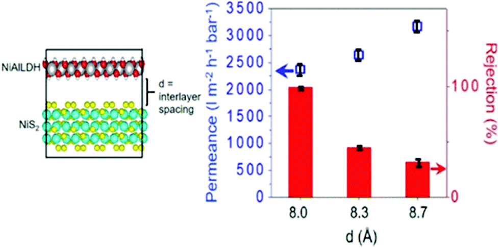 | ||
| Fig. 19 Left: Schematic presentation of control of the interlayer spacing of anionic TMD laminates using cationic layered double hydroxide (LDH) nanosheets. Right: Permeance and rejection of methyl orange (MO) dye in acetone through 250 ± 20 nm thick NiS2/NiAlLDH membranes as a function of the interlayer distance. Reproduced from ref. 130. | ||
This proposed hetero-assembly strategy using oppositely charged nanosheets is a very promising method to produce inorganic 2D-based membranes with a controllable interlayer distance for other gas or liquid separation applications.
5. Conclusions and future outlook
In this review, we have considered the various methods of solution-based bottom-up synthesis of TMDs and the properties of the resulting products. It was shown that these techniques enable the production of TMDs of varying shapes, sizes, morphologies, and phases, and we also gave some insight into how the variation of reaction conditions can affect these properties. It is clear that, if developed sufficiently, these synthetic methods may combine the cost-effectiveness and scalability of techniques such as LPE with the enhanced level of controllability provided by CVD, often at a fraction of the cost. The unique morphologies and phases that are readily obtained via these bottom-up synthetic regimes give rise to exciting applications as photocatalysts, anti-cancer and antibacterial agents, as well as for integration into electronics devices.The high quality and narrow size distribution of synthetic colloidal TMD-based nanomaterials, in combination with their unique physical and chemical properties, has resulted in significant advancements in the development of applications for these materials in recent years. It was demonstrated that 2D TMD materials are very promising for a range of biomedical applications including biosensing, drug delivery and photodynamic/photothermal therapy. However, despite the vast amount of progress made in recent years, and the obvious potential of these nanomaterials, they remain of academic interest only. One of the main concerns is the unknown potential toxicity of 2D nanostructures, which could limit their in vivo biomedical applications. The toxicity of 2D nanomaterials is still poorly studied and understood, and much detailed research on the biocompatibility and toxicity of TMD nanostructures is vital for their further advancement and use in biomedical applications.
TMDs possess unique catalytic properties which have been exploited in electro- and photocatalysis, in particular in the hydrogen evolution reaction (HER) and photo-oxidation of organic materials. However, further detailed experimental and theoretical studies are necessary to fully understand all phenomena, and to develop new, more efficient and selective catalysts, which will be crucial for the progression of relevant green chemistry sectors.
The 2D morphology and unique properties of TMDs such as semiconductor state, conductivity, flexibility, transparency and large surface area make these materials highly promising for future development of new wearable, flexible electronic devices. The promotion of synthetic colloidal TMD nanomaterials is especially important for these applications as they can be easily processed by standard solution and printing techniques, enabling new, cost-effective, flexible electronic devices.
2D TMD nanomaterials can also be tailored to form either fluorescent emitters or efficient fluorescence quenchers, making them powerful platforms for fabricating a series of optical sensors and biosensors to detect various targets, including gases, metal ions, biomolecules and potentially viral species. Despite the significant recent progress, TMD-based sensors still require further improvements in terms of detection limits and selectivity. The colloidal chemistry synthetic approaches offer excellent opportunities in this area, enabling the production of monolayers of photoluminescent TMD materials, which can be easily functionalised by standard wet chemistry techniques for targeted sensing applications. The photoluminescence properties of monolayered colloidal TMDs are also important for photonics applications, particularly in light emitting and laser devices.
TMD nanomaterials have emerging applications in energy harvesting and storage devices. The use of colloidal MoS2 and related materials as anodes in lithium ion batteries is particularly important. The bottom-up synthesis of TMDs enables the achievement of necessary control over size, phase and morphology of these nanomaterials and allows us to use efficient screen-printing techniques with colloidal inks, which are required for cost-effective production of batteries.
Colloidal synthetic 2D TMD nanomaterials are excellent materials for production of laminar membranes which are capable of providing exceptional performance and separation, even at very low membrane thickness. It has been shown that TMD-based membranes can outperform similar graphene oxide-based membranes of comparable thickness. The porosity of these membranes can be controlled and tuned by the dimensions of TMD flakes and by the addition of various interstitial nanoparticles or nanowires. In addition, these membrane materials can also be easily functionalised with appropriate groups to provide the necessary level of selectivity for targeted rejection and separation of mixtures of products. Thus, TMD-based membranes are expected to offer a number of advantages and their further development deserves significant attention.
Finally, the development of new chiral 2D TMD nanomaterials is expected to open up a vast range of new potential applications in valleytronics, spintronics, chiral sensing and asymmetric photocatalysis. However, the area of chiral 2D nanomaterials and their applications are minimally explored to date and this field is still in its infancy. Colloidal 2D TMD materials are excellent candidates for this research as chirality in these nanostructures can be induced by a simple synthesis in the presence of chiral ligands, or by the solution exchange of achiral ligands with appropriate enantiomeric molecules. Since chirality plays a crucial role in chemical and biological recognition and defines many interactions between chemical and biological species, these nanomaterials are also expected to have a significant impact on the fast-developing nano-biotechnology and nanomedicine disciplines.
Conflicts of interest
There are no conflicts to declare.Acknowledgements
The authors gratefully thank the Irish Research Council (projects: GOIPG/2019/2788) and the SFI Bioeconomy Research Centre, Biorbic (project: SFI 16/RC/3889) for financial support.References
- K. S. Novoselov, A. K. Geim, S. v. Morozov, D. Jiang, Y. Zhang, S. v. Dubonos, I. v. Grigorieva and A. A. Firsov, Science, 2004, 306, 666–669 CrossRef CAS PubMed.
- Y. Hernandez, V. Nicolosi, M. Lotya, F. M. Blighe, Z. Sun, S. De, I. T. McGovern, B. Holland, M. Byrne, Y. K. Gun’ko, J. J. Boland, P. Niraj, G. Duesberg, S. Krishnamurthy, R. Goodhue, J. Hutchison, V. Scardaci, A. C. Ferrari and J. N. Coleman, Nat. Nanotechnol., 2008, 3, 563–568 CrossRef CAS PubMed.
- J. N. Coleman, M. Lotya, A. O’Neill, S. D. Bergin, P. J. King, U. Khan, K. Young, A. Gaucher, S. De, R. J. Smith, I. v. Shvets, S. K. Arora, G. Stanton, H. Y. Kim, K. Lee, G. T. Kim, G. S. Duesberg, T. Hallam, J. J. Boland, J. J. Wang, J. F. Donegan, J. C. Grunlan, G. Moriarty, A. Shmeliov, R. J. Nicholls, J. M. Perkins, E. M. Grieveson, K. Theuwissen, D. W. McComb, P. D. Nellist and V. Nicolosi, Science, 2011, 331, 568–571 CrossRef CAS PubMed.
- C. Ataca, H. Şahin and S. Ciraci, J. Phys. Chem. C, 2012, 116, 8983–8999 CrossRef CAS.
- K. F. Mak, C. Lee, J. Hone, J. Shan and T. F. Heinz, Phys. Rev. Lett., 2010, 105, 136805 CrossRef PubMed.
- A. Splendiani, L. Sun, Y. Zhang, T. Li, J. Kim, C.-Y. Chim, G. Galli and F. Wang, Nano Lett., 2010, 10, 1271–1275 CrossRef CAS PubMed.
- H. Tian, J. Tice, R. Fei, V. Tran, X. Yan, L. Yang and H. Wang, Nano Today, 2016, 11, 763–777 CrossRef CAS.
- A. Soni, C. M. Pandey, M. K. Pandey and G. Sumana, Anal. Chim. Acta, 2019, 1055, 26–35 CrossRef CAS PubMed.
- Y. Xu, H. Cao, Y. Xue, B. Li and W. Cai, Nanomaterials, 2018, 8, 942 CrossRef PubMed.
- M. Bodík, A. Annušová, J. Hagara, M. Mičušík, M. Omastová, M. Kotlár, J. Chlpík, J. Cirák, H. Švajdlenková, M. Anguš, A. M. Roldán, P. Veis, M. Jergel, E. Majkova and P. Šiffalovič, Phys. Chem. Chem. Phys., 2019, 21, 12396–12405 RSC.
- C. Backes, B. M. Szydłowska, A. Harvey, S. Yuan, V. Vega-Mayoral, B. R. Davies, P. L. Zhao, D. Hanlon, E. J. G. Santos, M. I. Katsnelson, W. J. Blau, C. Gadermaier and J. N. Coleman, ACS Nano, 2016, 10, 1589–1601 CrossRef CAS PubMed.
- Q. Fu, W. Wang, L. Yang, J. Huang, J. Zhang and B. Xiang, RSC Adv., 2015, 5, 15795–15799 RSC.
- M. H. Khan, H. K. Liu, X. Sun, Y. Yamauchi, Y. Bando, D. Golberg and Z. Huang, Mater. Today, 2017, 20, 611–628 CrossRef CAS.
- W. Liu, H. Li, C. Xu, Y. Khatami and K. Banerjee, Carbon, 2011, 49, 4122–4130 CrossRef CAS.
- J. A. Wilson and A. D. Yoffe, Adv. Phys., 1969, 18, 193–335 CrossRef CAS.
- G. W. Morey and P. Niggli, J. Am. Chem. Soc., 1913, 35, 1086–1130 CrossRef CAS.
- T. Dubois and G. Demazeau, Mater. Lett., 1994, 19, 38–47 CrossRef CAS.
- J. H. Zhan, Z. D. Zhang, X. F. Qian, C. Wang, Y. Xie and Y. T. Qian, J. Solid State Chem., 1998, 141, 270–273 CrossRef CAS.
- R. Fan, X. Chen and Z. Chen, Chem. Lett., 2000, 920–921 CrossRef CAS.
- H. A. Therese, J. Li, U. Kolb and W. Tremel, Solid State Sci., 2005, 7, 67–72 CrossRef CAS.
- D. Chakravarty and D. J. Late, RSC Adv., 2015, 5, 21700–21709 RSC.
- Y. Liu, N. Zhang, H. Kang, M. Shang, L. Jiao and J. Chen, Chem. – Eur. J., 2015, 21, 11878–11884 CrossRef CAS PubMed.
- P. P. Wang, H. Sun, Y. Ji, W. Li and X. Wang, Adv. Mater., 2014, 26, 964–969 CrossRef CAS PubMed.
- V. K. Lamer and R. H. Dinegar, J. Am. Chem. Soc., 1950, 72, 4847–4854 CrossRef CAS.
- C. B. Murray, D. J. Norris and M. G. Bawendi, J. Am. Chem. Soc., 1993, 115, 8706–8715 CrossRef CAS.
- X. Bai, F. Purcell-Milton and Y. Gun’ko, Nanomaterials, 2019, 9, 85 CrossRef PubMed.
- C. B. Murray, C. R. Kagan and M. G. Bawendi, Annu. Rev. Mater. Sci., 2000, 30, 545–610 CrossRef CAS.
- A. Ghorai, A. Midya and S. K. Ray, New J. Chem., 2018, 42, 3609–3613 RSC.
- A. Bayat and E. Saievar-Iranizad, J. Lumin., 2017, 185, 236–240 CrossRef CAS.
- L. Zhou, S. Yan, H. Wu, H. Song and Y. Shi, Catalysts, 2017, 7, 18 CrossRef.
- A. Ghorai, S. Bayan, N. Gogurla, A. Midya and S. K. Ray, ACS Appl. Mater. Interfaces, 2017, 9, 558–565 CrossRef CAS PubMed.
- W. Yin, X. Bai, P. Chen, X. Zhang, L. Su, C. Ji, H. Gao, H. Song and W. W. Yu, ACS Appl. Mater. Interfaces, 2018, 10, 43824–43830 CrossRef CAS PubMed.
- M. S. Sokolikova, P. C. Sherrell, P. Palczynski, V. L. Bemmer and C. Mattevi, Nat. Commun., 2019, 10, 1–8 CrossRef PubMed.
- N. Savjani, E. A. Lewis, M. A. Bissett, J. R. Brent, R. A. W. Dryfe, S. J. Haigh and P. O’Brien, Chem. Mater., 2016, 28, 657–664 CrossRef CAS.
- W. Jung, S. Lee, D. Yoo, S. Jeong, P. Miró, A. Kuc, T. Heine and J. Cheon, J. Am. Chem. Soc., 2015, 137, 7266–7269 CrossRef CAS PubMed.
- P. Zhou, I. Tanghe, P. Schiettecatte, D. van Thourhout, Z. Hens and P. Geiregat, J. Chem. Phys., 2019, 151, 164701 CrossRef PubMed.
- W. Zhao, Z. Ghorannevis, K. K. Amara, J. R. Pang, M. Toh, X. Zhang, C. Kloc, P. H. Tan and G. Eda, Nanoscale, 2013, 5, 9677–9683 RSC.
- A. Berkdemir, H. R. Gutiérrez, A. R. Botello-Méndez, N. Perea-López, A. L. Elías, C. I. Chia, B. Wang, V. H. Crespi, F. López-Urías, J. C. Charlier, H. Terrones and M. Terrones, Sci. Rep., 2013, 3, 1–8 Search PubMed.
- J. Q. Geisenhoff, A. K. Tamura and A. M. Schimpf, Chem. Commun., 2019, 55, 8856–8859 RSC.
- J. W. Seo, Y. W. Jun, S. W. Park, H. Nah, T. Moon, B. Park, J. G. Kim, Y. J. Kim and J. Cheon, Angew. Chem., Int. Ed., 2007, 46, 8828–8831 CrossRef CAS PubMed.
- R. Mastria, R. Scarfiello, D. Altamura, C. Giannini, A. Liscio, A. Kovtun, G. V. Bianco, G. Bruno, V. Grillo, A. H. Tavabi, R. E. Dunin-Borkowski, C. Nobile, A. Cola, P. D. Cozzoli, S. Gambino and A. Rizzo, Sci. Rep., 2019, 9, 1–13 CAS.
- X. Ding, F. Peng, J. Zhou, W. Gong, G. Slaven, K. P. Loh, C. T. Lim and D. T. Leong, Nat. Commun., 2019, 10, 1–13 CrossRef PubMed.
- V. Štengl and J. Henych, Nanoscale, 2013, 5, 3387–3394 RSC.
- P. Sharma, A. Kumar, S. Bankuru, J. Chakraborty and S. Puravankara, New J. Chem., 2020, 44, 1594–1608 RSC.
- N. Kumar, B. P. A. George, H. Abrahamse, V. Parashar and J. C. Ngila, Appl. Surf. Sci., 2017, 396, 8–18 CrossRef CAS.
- S. Masimukku, Y. C. Hu, Z. H. Lin, S. W. Chan, T. M. Chou and J. M. Wu, Nano Energy, 2018, 46, 338–346 CrossRef CAS.
- M. B. Askari, A. F. Kalourazi, M. Seifi, S. S. Shahangian, N. Askari and T. J. Manjili, Optik, 2018, 174, 154–162 CrossRef CAS.
- J. Wang, N. Wang, Y. Guo, J. Yang, J. Wang, F. Wang, J. Sun, H. Xu, Z. H. Liu and R. Jiang, ACS Sustainable Chem. Eng., 2018, 6, 13435–13442 CrossRef CAS.
- J. Xie, H. Zhang, S. Li, R. Wang, X. Sun, M. Zhou, J. Zhou, X. W. Lou and Y. Xie, Adv. Mater., 2013, 25, 5807–5813 CrossRef CAS PubMed.
- H. Chu, X. Liu, B. Liu, G. Zhu, W. Lei, H. Du, J. Liu, J. Li, C. Li and C. Sun, Sci. Rep., 2016, 6, 1–10 CrossRef PubMed.
- Y. Lu, X. Yao, J. Yin, G. Peng, P. Cui and X. Xu, RSC Adv., 2015, 5, 7938–7943 RSC.
- F. Giubileo, A. Grillo, M. Passacantando, F. Urban, L. Iemmo, G. Luongo, A. Pelella, M. Loveridge, L. Lozzi and A. di Bartolomeo, Nanomaterials, 2019, 9, 717 CrossRef CAS PubMed.
- N. T. Thang, L. T. Hong, N. H. Thoan, C. M. Hung, N. van Duy, N. van Hieu and N. D. Hoa, RSC Adv., 2020, 10, 12759–12771 RSC.
- Y. Sun, W. He, X. Sun and B. Liu, Luminescence, 2020, 1–8, DOI:10.1002/bio.3906.
- Y. Sun, J. Xu, Z. Zhu, Y. Wang, H. Xia, Z. You, C. Lee and C. Tu, Opt. Mater. Express, 2015, 5, 2924 CrossRef CAS.
- Y. Wang, F. Zhang, Q. Wang, P. Yang, H. Lin and F. Qu, Nanoscale, 2018, 10, 14534–14545 RSC.
- D. Son, S. I. Chae, M. Kim, M. K. Choi, J. Yang, K. Park, V. S. Kale, J. H. Koo, C. Choi, M. Lee, J. H. Kim, T. Hyeon and D.-H. Kim, Adv. Mater., 2016, 28, 9326–9332 CrossRef CAS PubMed.
- P. Schiettecatte, P. Geiregat and Z. Hens, J. Phys. Chem. C, 2019, 123, 10571–10577 CrossRef CAS.
- S. Barua, H. S. Dutta, S. Gogoi, R. Devi and R. Khan, ACS Appl. Nano Mater., 2018, 1, 2–25 CrossRef CAS.
- H. Laroui, D. S. Wilson, G. Dalmasso, K. Salaita, N. Murthy, S. v. Sitaraman and D. Merlin, Am. J. Physiol., 2011, 300, G371–G383 CAS.
- V. Agarwal and K. Chatterjee, Nanoscale, 2018, 10, 16365–16397 RSC.
- J. v. Jokerst, T. Lobovkina, R. N. Zare and S. S. Gambhir, Nanomedicine, 2011, 6, 715–728 CrossRef CAS.
- P. Milla, F. Dosio and L. Cattel, Curr. Drug Metab., 2012, 13, 105–119 CrossRef CAS PubMed.
- Z. Xie, Y. Duo, Z. Lin, T. Fan, C. Xing, L. Yu, R. Wang, M. Qiu, Y. Zhang, Y. Zhao, X. Yan and H. Zhang, Adv. Sci., 2020, 7, 1902236 CrossRef CAS PubMed.
- H. Chen, T. Liu, Z. Su, L. Shang and G. Wei, Nanoscale Horiz., 2018, 3, 74–89 RSC.
- A. Doughty, A. Hoover, E. Layton, C. Murray, E. Howard and W. Chen, Materials, 2019, 12, 779 CrossRef CAS PubMed.
- C. Wang, J. Bai, Y. Liu, X. Jia and X. Jiang, ACS Biomater. Sci. Eng., 2016, 2, 2011–2017 CrossRef CAS PubMed.
- Z. Lei, W. Zhu, S. Xu, J. Ding, J. Wan and P. Wu, ACS Appl. Mater. Interfaces, 2016, 8, 20900–20908 CrossRef CAS PubMed.
- X. Yang, J. Li, T. Liang, C. Ma, Y. Zhang, H. Chen, N. Hanagata, H. Su and M. Xu, Nanoscale, 2014, 6, 10126–10133 RSC.
- R. Parsons, Trans. Faraday Soc., 1958, 54, 1053–1063 RSC.
- B. Hinnemann, P. G. Moses, J. Bonde, K. P. Jørgensen, J. H. Nielsen, S. Horch, I. Chorkendorff and J. K. Nørskov, J. Am. Chem. Soc., 2005, 127, 5308–5309 CrossRef CAS PubMed.
- A. B. Laursen, S. Kegnæs, S. Dahl and I. Chorkendorff, Energy Environ. Sci., 2012, 5, 5577–5591 RSC.
- V. Nguyen, T. P. Nguyen, T. Le, D. N. Vo, D. L. Nguyen, Q. T. Trinh, I. T. Kim and Q. van Le, J. Chem. Technol. Biotechnol., 2020, 95, 2597–2607 CAS.
- S. S. Chou, N. Sai, P. Lu, E. N. Coker, S. Liu, K. Artyushkova, T. S. Luk, B. Kaehr and C. J. Brinker, Nat. Commun., 2015, 6, 1–8 Search PubMed.
- S. Jayabal, J. Wu, J. Chen, D. Geng and X. Meng, Mater. Today Energy, 2018, 10, 264–279 CrossRef.
- D. Voiry, A. Mohite and M. Chhowalla, Chem. Soc. Rev., 2015, 44, 2702–2712 RSC.
- W. Zhou, X. Zou, S. Najmaei, Z. Liu, Y. Shi, J. Kong, J. Lou, P. M. Ajayan, B. I. Yakobson and J. C. Idrobo, Nano Lett., 2013, 13, 2615–2622 CrossRef CAS PubMed.
- N. García Doménech, F. Purcell-Milton and Y. K. Gun’ko, Mater. Today Commun., 2020, 23, 100888 CrossRef.
- X. He and P. Li, Exposure Health, 2020, 12, 385–401 CrossRef CAS.
- S. Mishra and R. N. Bharagava, J. Environ. Sci. Health, Part C: Environ. Carcinog. Ecotoxicol. Rev., 2016, 34, 1–32 CrossRef CAS PubMed.
- M. Giagnorio, S. Steffenino, L. Meucci, M. C. Zanetti and A. Tiraferri, J. Environ. Chem. Eng., 2018, 6, 4467–4475 CrossRef CAS.
- G. Reina, J. M. González-Domínguez, A. Criado, E. Vázquez, A. Bianco and M. Prato, Chem. Soc. Rev., 2017, 46, 4400–4416 RSC.
- S. Tang, W. Wu, X. Xie, X. Li and J. Gu, RSC Adv., 2017, 7, 9862–9871 RSC.
- Z. Qian, L. Jiao and L. Xie, Chin. J. Chem., 2020, 38, 753–760 CrossRef CAS.
- A. A. Green and M. C. Hersam, J. Phys. Chem. Lett., 2010, 1, 544–549 CrossRef CAS PubMed.
- M. G. Stanford, P. D. Rack and D. Jariwala, npj 2D Mater. Appl., 2018, 2, 20 CrossRef.
- S. Jeong, D. Yoo, M. Ahn, P. Miro, T. Heine and J. Cheon, Nat. Commun., 2015, 6, 1–7 Search PubMed.
- J. Li, M. C. Lemme and M. Östling, ChemPhysChem, 2014, 15, 3427–3434 CrossRef CAS.
- J. Wang and B. Liu, Sci. Technol. Adv. Mater., 2019, 20, 992–1009 CrossRef PubMed.
- D. Ovchinnikov, A. Allain, Y. S. Huang, D. Dumcenco and A. Kis, ACS Nano, 2014, 8, 8174–8181 CrossRef CAS PubMed.
- R. H. Fowler and L. Nordheim, Proc. R. Soc. London, Ser. A, 1928, 119, 173–181 CAS.
- F. Giubileo, A. di Bartolomeo, L. Iemmo, G. Luongo and F. Urban, Appl. Sci., 2018, 8, 526 CrossRef.
- F. Urban, M. Passacantando, F. Giubileo, L. Iemmo and A. di Bartolomeo, Nanomaterials, 2018, 8(3), 151 CrossRef PubMed.
- W. B. Choi, D. S. Chung, J. H. Kang, H. Y. Kim, Y. W. Jin, I. T. Han, Y. H. Lee, J. E. Jung, N. S. Lee, G. S. Park and J. M. Kim, Appl. Phys. Lett., 1999, 75, 3129–3131 CrossRef CAS.
- R. Yabushita, K. Hata, H. Sato and Y. Saito, J. Vac. Sci. Technol., B: Microelectron. Nanometer Struct.–Process., Meas., Phenom., 2007, 25, 640 CrossRef CAS.
- T. Cao, G. Wang, W. Han, H. Ye, C. Zhu, J. Shi, Q. Niu, P. Tan, E. Wang, B. Liu and J. Feng, Nat. Commun., 2012, 3, 1–5 Search PubMed.
- K. F. Mak, K. He, J. Shan and T. F. Heinz, Nat. Nanotechnol., 2012, 7, 494–498 CrossRef CAS.
- W. Yao, D. Xiao and Q. Niu, Phys. Rev. B: Condens. Matter Mater. Phys., 2008, 77, 235406 CrossRef.
- F. Purcell-Milton, R. McKenna, L. J. Brennan, C. P. Cullen, L. Guillemeney, N. v. Tepliakov, A. S. Baimuratov, I. D. Rukhlenko, T. S. Perova, G. S. Duesberg, A. v. Baranov, A. v. Fedorov and Y. K. Gun’Ko, ACS Nano, 2018, 12, 954–964 CrossRef CAS PubMed.
- V. Galstyan, Sensors, 2017, 17, 2947 CrossRef PubMed.
- A. J. Bandodkar, I. Jeerapan and J. Wang, ACS Sens., 2016, 1, 464–482 CrossRef CAS.
- M. C. Domingo, J. Network Comput. Appl., 2012, 35, 584–596 CrossRef.
- W. Yang, L. Gan, H. Li and T. Zhai, Inorg. Chem. Front., 2016, 3, 433–451 RSC.
- D. J. Late, Y. K. Huang, B. Liu, J. Acharya, S. N. Shirodkar, J. Luo, A. Yan, D. Charles, U. v. Waghmare, V. P. Dravid and C. N. R. Rao, ACS Nano, 2013, 7, 4879–4891 CrossRef CAS PubMed.
- W. Yin, X. Dong, J. Yu, J. Pan, Z. Yao, Z. Gu and Y. Zhao, ACS Appl. Mater. Interfaces, 2017, 9, 21362–21370 CrossRef CAS PubMed.
- D. Qiu, Y. Chu, H. Zeng, H. Xu and G. Dan, ACS Appl. Mater. Interfaces, 2019, 11, 37035–37042 CrossRef CAS PubMed.
- A. Ganeshpurkar and A. K. Saluja, Saudi Pharm. J., 2017, 25, 149–164 CrossRef PubMed.
- F. Yi, H. Ren, J. Shan, X. Sun, D. Wei and Z. Liu, Chem. Soc. Rev., 2018, 47, 3152–3188 RSC.
- J. R. Sootsman, D. Y. Chung and M. G. Kanatzidis, Angew. Chem., Int. Ed., 2009, 48, 8616–8639 CrossRef CAS PubMed.
- Y. Xie, T. M. Chou, W. Yang, M. He, Y. Zhao, N. Li and Z. H. Lin, Semicond. Sci. Technol., 2017, 32, 044003 CrossRef.
- D. D. Fan, H. J. Liu, L. Cheng, P. H. Jiang, J. Shi and X. F. Tang, Appl. Phys. Lett., 2014, 105, 133113 CrossRef.
- C. Shang, Y. Zhang, H. Qin, B. He, C. Zhang, J. Sun, J. Li, J. Ma, X. Ji, L. Xu and B. Fu, Opt. Laser Technol., 2020, 131, 106375 CrossRef CAS.
- Z. Luo, D. Wu, B. Xu, H. Xu, Z. Cai, J. Peng, J. Weng, S. Xu, C. Zhu, F. Wang, Z. Sun and H. Zhang, Nanoscale, 2016, 8, 1066–1072 RSC.
- A. Martinez and Z. Sun, Nat. Photonics, 2013, 7, 842–845 CrossRef CAS.
- W. Jie, Z. Yang, G. Bai and J. Hao, Adv. Opt. Mater., 2018, 6, 1701296 CrossRef.
- W. Zhao, Z. Ghorannevis, L. Chu, M. Toh, C. Kloc, P. H. Tan and G. Eda, ACS Nano, 2013, 7, 791–797 CrossRef CAS PubMed.
- S. Mouri, Y. Miyauchi and K. Matsuda, Nano Lett., 2013, 13, 5944–5948 CrossRef CAS PubMed.
- M. Amani, D. H. Lien, D. Kiriya, J. Xiao, A. Azcatl, J. Noh, S. R. Madhvapathy, R. Addou, K. C. Santosh, M. Dubey, K. Cho, R. M. Wallace, S. C. Lee, J. H. He, J. W. Ager, X. Zhang, E. Yablonovitch and A. Javey, Science, 2015, 350, 1065–1068 CrossRef CAS PubMed.
- A. Pospischil, M. M. Furchi and T. Mueller, Nat. Nanotechnol., 2014, 9, 257–261 CrossRef CAS PubMed.
- J. L. O’Brien, A. Furusawa and J. Vučković, Nat. Photonics, 2009, 3, 687–695 CrossRef.
- Y. J. Zhang, T. Oka, R. Suzuki, J. T. Ye and Y. Iwasa, Science, 2014, 344, 725–728 CrossRef CAS PubMed.
- G. Liu, W. Jin and N. Xu, Angew. Chem., Int. Ed., 2016, 55, 13384–13397 CrossRef CAS PubMed.
- L. Sun, Y. Ying, H. Huang, Z. Song, Y. Mao, Z. Xu and X. Peng, ACS Nano, 2014, 8, 6304–6311 CrossRef CAS PubMed.
- L. Sun, H. Huang and X. Peng, Chem. Commun., 2013, 49, 10718–10720 RSC.
- M. Samadi, N. Sarikhani, M. Zirak, H. Zhang, H. L. Zhang and A. Z. Moshfegh, Nanoscale Horiz., 2018, 3, 90–204 RSC.
- Y. Abate, D. Akinwande, S. Gamage, H. Wang, M. Snure, N. Poudel and S. B. Cronin, Adv. Mater., 2018, 30, 1704749 CrossRef PubMed.
- R. Ma and T. Sasaki, Acc. Chem. Res., 2015, 48, 136–143 CrossRef CAS PubMed.
- G. Liu, W. Jin and N. Xu, Angew. Chem., Int. Ed., 2016, 55, 13384–13397 CrossRef CAS PubMed.
- K. S. Novoselov, A. Mishchenko, A. Carvalho and A. H. Castro Neto, Science, 2016, 353 Search PubMed.
- E. H. Ang and J. W. Chew, Chem. Mater., 2019, 31, 10002–10007 CrossRef CAS.
- H. M. Tham, S. Japip and T. S. Chung, J. Membr. Sci., 2019, 588, 117219 CrossRef CAS.
| This journal is © The Royal Society of Chemistry 2021 |