
 Open Access Article
 This Open Access Article is licensed under a Creative Commons Attribution-Non Commercial 3.0 Unported Licence
Comparison of diverse resistive switching characteristics and demonstration of transitions among them in Al-incorporated HfO2-based resistive switching memory for neuromorphic applications†
Sobia Ali Khana and
Sungjun Kim *b
*b
aSchool of Electronics Engineering, Chungbuk National University, Cheongju 28644, South Korea
bDivision of Electronics and Electrical Engineering, Dongguk University, Seoul 04620, South Korea. E-mail: sungjun@dongguk.edu
First published on 24th August 2020
Abstract
Diverse resistive switching behaviors are observed in the Pt/HfAlOx/TiN memory device depending on the compliance current, the sweep voltage amplitude, and the bias polarity. We extensively compare three types of resistive switching characteristics in a Pt/HfAlOx/TiN device in terms of endurance, ON/OFF ratio, linear conductance update, and read margin in a cross-point array structure for synaptic device applications. The bipolar resistive switching under positive set and negative reset shows better linear synaptic weight updates due to gradual switching than the bipolar resistive switching at the opposite polarity. The complementary resistive switching shows a higher read margin due to the current suppression at a low voltage regime. In addition, the potentiation and the depression can be adjusted at the same voltage polarity for a hardware neuromorphic system. Finally, we demonstrate the transition between bipolar resistive switching and complementary resistive switching, which could provide flexibility for different applications.
Introduction
Compared to traditional non-volatile memories1 such as NAND Flash, resistive switching memory (RRAM) is considered to be more promising in terms of its low power consumption2 and fast switching speed.3 It is also quite competitive in terms of scalability and multi-level cells (MLC).4 RRAM shows different types of resistive switching from various insulating mediums such as metal oxide,5 semiconductor materials, organic materials, and 2D materials.6 The switching behaviors are mainly classified into progressive switching and abrupt switching during set and reset. Progressive switching is particularly suitable for MLC implementation in non-volatile memory applications.7 Multi-conductance-states in an RRAM device are also extensively utilized as electronic synapses in neuromorphic systems,8 which have the potential to replace von Neumann computing in the near future. Neuromorphic engineering emulates a neuro-biological architecture to implement an energy-efficient computing system with parallel data processing. Non-volatile memory devices such as Flash memory9 and resistance-type new memories can act as biological synapses in a nervous system by storing and change the weight for a long time.10 Among them, RRAM-based artificial electronic synapses have shown many attractive benefits in neuromorphic computing,11 i.e., a simple structure, low energy consumption,12 multi-level storage,13 and good CMOS compatibility14 with high-density integration.14The resistive switching is largely divided into three categories. Unipolar resistive switching (URS) occurs in the same polarity in which the reset process uses Joule heating with high current. Bipolar resistive switching (BRS) occurs in different polarities, which is dominantly driven by electric field. The reset is completed after set process in the same polarity for complementary resistive switching (CRS).13
Among the many resistive switching materials, HfO2 is a well-proven material with excellent reproducibility and repeatability, and it has been studied for a long time for non-volatile storage memory applications as well as for high-k gate dielectrics in CMOS.15,16 However, the defect controlled switching-based RRAM devices including metal oxides cannot avoid the variation of switching parameters because of the stochastic nature.17
Several approaches have been applied to further improve the non-volatile memory properties of HfO2 RRAM. The dopant of another material such as Al into an HfO2 layer or the bilayer Al2O3/HfO2 structure can enhance the uniformity of set and reset switching by stabilizing the conductive filament.18–21 The use of Al2O3,19 which has a larger band gap than HfO2, can lead to improved resistive switching properties, such as low power consumption and nonlinear I–V.19 Furthermore, synaptic characteristics have been reported in several HfO2-based RRAM devices.7,21
In this work, we characterize the various resistive switching behaviors of an Al-doped HfO2 (HfAlOx)-based RRAM device for neuromorphic computing. The switching behaviors are classified into three types by controlling the compliance current (CC) and the voltage polarity. A single device that can have various resistive switching characteristics determined by the operating conditions is advantageous in the sense that it can be flexibly applied to various applications. Two bipolar resistive switching at positive set and negative set and a complementary resistive switching are evaluated in terms of the ON/OFF ratio, endurance cycle, read margin, and the nonlinearity and variation of potentiation and depression for synaptic device application in a hardware based-neuromorphic system. In addition, we experimentally demonstrate the transition between BRS and CRS.
Experimental section
The Pt/HfAlOx/TiN device was fabricated as follows. A 100 nm-thick TiN was deposited by DC sputtering on a SiO2/Si wafer. A 7 nm-thick high-k HfAlOx film was then accurately deposited by atomic layer deposition (ALD). The HfO2 layer reacted with TEMAHf and H2O. One cycle is composed of TEMAHf (0.5 s)-purse (35 s)-H2O (0.3 s)-purge (35 s) for ALD HfO2 layer. The Al2O3 reacted with TEMAH and H2O. The Al2O3 layer reacted with TMA and H2O. One cycle is composed of TMA (0.2 s)-purse (15 s)-H2O (0.2 s)-purge (15 s) for ALD Al2O3 layer. For the HfAlOx film, one cycle of HfO2 and then five cycles of Al2O3 were alternately deposited for a total of 15 times. Next, a 100 nm thick Pt top electrode was deposited by an e-beam evaporator and patterned by a shadow mask containing circular patterns with a diameter of 100 μm. All the electrical properties, including the DC and transient characteristics, were used with a Keithley 4200-SCS semiconductor parameter analyzer and in pulse mode using a 4225-PMU ultrafast module. All measurements were performed at room temperature and ambient atmosphere. The bias was applied on the Pt top electrode while the TiN bottom electrode was grounded.Results and discussion
Fig. 1(a) shows the structure of the Pt/HfAlOx/TiN device. The device stack is well confirmed by the high-resolution transmission electron microscope (HRTEM) image shown in Fig. 1(b). Further, each element (Pt, Hf, Al, O, Ti, and N) is well scanned by energy dispersive X-ray spectroscopy (EDS) analysis, as illustrated in Fig. 1(c). | ||
| Fig. 1 Device configuration of Pt/HfAlOx/TiN device: (a) schematic of the device stack, (b) HRTEM image, (c) EDS line scan. | ||
First, DC bias sweeps are applied to the device to characterize its typical I–V curves for electrical analysis, as shown in Fig. 2(a). The initial forming-free behavior on pristine cell and high resistance state (HRS) are found. After applying the CC of 700 μA, the Pt/HfAlOx/TiN device shows stable BRS up to 200 cycles with an ON/OFF ratio of about 10 at 0.5 V. The device switches from HRS to low resistance state (LRS) at about −1.5 V for the set process. The device starts to return to HRS with positive sweep for reset. Note that this switching (negative set and positive reset) is classified as type 1 (BRS1) in this work. The multi-level states in the RRAM cell can increase the memory density at the same cell size, which is useful for storage memory applications.22 Moreover, MLC improves the computing system performance in hardware neuromorphic systems.23 Fig. 2(b) shows the multi-level switching by controlling reset voltage switching. The set process occurs in an abrupt manner, and it is relatively difficult to control the set voltage for MLC.24 Conversely, after the set process, the current gradually decreases by a continuous reset process while positively increasing the step voltage of 0.1 V. HRS and LRS follow Schottky emission and ohmic conduction, respectively, as reported in the previous literature25,26 (see Fig. S1, ESI†).
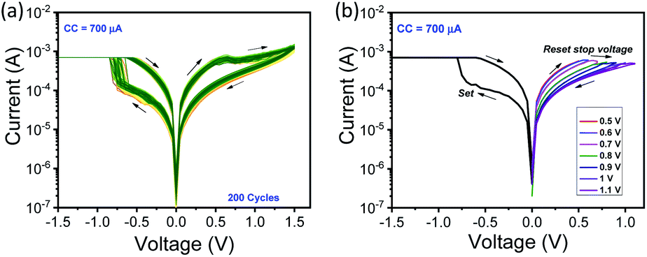 | ||
| Fig. 2 (a) I–V characteristics of the Pt/HfAlOx/TiN device by negative set and positive reset (type 1, BRS1). (b) Multilevel I–V curves by reset stop voltage from 0.5 V to 1.1 V. | ||
For more practical memory switching operation, pulse measurements are conducted on the Pt/HfAlOx/TiN device. Fig. 3(a) shows the set and reset transient switching driven by voltage pulse input. The low current at the initial state is monitored by read pulse (0.2 V, 100 μs), and the current increases by the same read voltage after the set pulse (−0.8 V, 100 μs) is applied. Similarly, the current decreases are confirmed by the same read pulse after reset pulse (1 V, 100 μs). The endurance is conducted by up to 100 cycles for transitions between two states (ON: about 1 kΩ, OFF: 2 kΩ–2.8 kΩ) by applying the pulse scheme displayed in Fig. 3(a), as shown in Fig. 3(b). The ON/OFF ratio can be increased by using higher voltage amplitude. The multi-level conductance values are obtained by varying the voltage amplitudes (−0.7 V to −1.15 V) with an identical pulse width of 100 μs for the set process, and by varying the voltage amplitudes (0.9 V–1.3 V) for the reset process.
 | ||
| Fig. 3 Pulse responses of the Pt/HfAlOx/TiN device in type 1. (a) Set and reset switching in pulse mode, (b) endurance cycle in pulse mode, (c) MLC with difference conductance levels driven by pulse response. | ||
Next, we emulate important biological synapse functions, such as long-term potentiation (LTP), long-term depression (LTD), and paired pulse facilitation (PPF), in a Pt/HfAlOx/TiN device, an artificial electronic device.27 Fig. 4(a) shows a schematic of a biological synapse, a pre-synaptic neuron, and a post-synaptic neuron. The synapse acting as neuronal junction or bridge controls the electrical or chemical signal between two neurons.28 Synapses regulate connection strength and are involved in learning and memory in the human brain. Similarly, the metal–insulator–metal (MIM) capacitance structure can facilitate weight (conductance) adjustment through external pulse inputs.29 LTP and LTD are key features for adjusting the neuronal synaptic plasticity.30 Fig. 4(b) shows the LTP and LTD curve driven by each of the identical 50 pulses. Fifty consecutive conductance values are measured at a VREAD of 0.2 V after potentiating the set pulse (−1.3 V, 100 μs). For LTD, depressing reset pulses (1.5 V, 100 μs) and a VREAD of 0.2 V are used. The conductance values are tuned from 1.116 mS to 2.028 mS. In the LTP, the conductance is significantly changed at the beginning of the pulse and a large variation is observed. The variation of LTP and LTD is due to the stochastic behaviors from resistive switching using the movement of oxygen vacancies. Especially, the potentiation (set process) has large variation due to the abrupt change in filamentary type.17
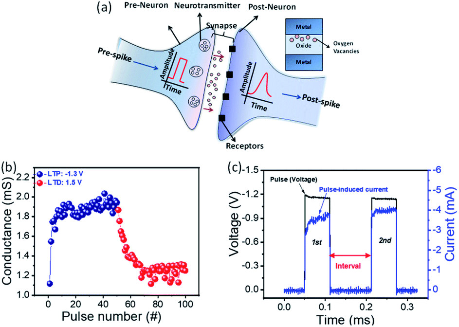 | ||
| Fig. 4 Synaptic characteristics of the Pt/HfAlOx/TiN device in type 1. (a) Schematic of the biological synapse between pre-neuron and post-neuron, (b) change in the conductance of 100 consecutive identical pulse responses for LTP and LTD, (c) PPF function emulated by artificial electron device. | ||
The LTP curve is consistent with the abrupt set process of the I–V curve shown in Fig. 2(a). There are large variations in the LTP and LTD curves. For example, the conductance in some points decreases with the set pulse and increases with the reset pulse. Next, we emulate PPF, which is associated with short-term plasticity.31 The second current is higher than the first one when two identical paired pulses (voltage: −1.3 V, width: 100 μs) are applied on the artificial synaptic device (Pt/HfAlOx/TiN device). This enhancement, which is also known as facilitation in the nervous system, occurs because the interval time is shorter than the recovery time and the device has a non-volatile property.32
Resistive switching also occurs in the Pt/HfAlOx/TiN device at the positive set and negative reset process, which is defined as type 2 (BRS2). Fig. 5(a) shows the typical type 2 BRS characteristics. The more gradual switching is observed for set switching, so we can control the set stop voltage (0.6 V to 0.72 V) as well as the reset stop voltage (−1 V to −1.44 V) to obtain different current levels, as shown in Fig. 5(b). In addition, LTP and LTD are obtained in a similar manner for type 1. Here, 50 consecutive increases in conductance for LTP (0.9 V, 100 μs) and 50 decreases in conductance for LTD (−1.6 V, 100 μs) are controlled to confirm the synaptic plasticity of the artificial electronic synapse.33 The conductance values are varied from 1.589 mS to 2.966 mS with substantially lower fluctuation than that used in type 1.
 | ||
| Fig. 5 (a) BRS I–V characteristics of the Pt/HfAlOx/TiN device by positive-set and negative set (type 2, BRS2), (b) MLC characteristics by controlling set (positive bias) and reset (negative bias) stop voltages, (c) LTP and LTD curve by identical pulses (LTP: 0.9 V and LTD: −1.6 V). | ||
To evaluate the CC effect on resistive switching behaviours, a high CC of 2 mA is applied on a pristine cell by DC voltage sweep in a negative regime. The device shows an extraordinary CRS.34 The repeatable CRS up to 50 consecutive cycles is obtained; here, the set occurs first, then the reset occurs at a larger voltage in the same polarity at both positive and negative regimes. Unlike conventional BRS, the CRS has the advantage of suppressing leakage current when applying a half-bias scheme in a cross-point structure, because the current is suppressed at a low voltage regime before the set process.35 Moreover, to emulate the synaptic behaviour in the CRS curve, we design the applied voltage with different amplitudes at the same polarity. The conductance levels for the LTP and LTD curve are well controlled by 50 identical pulse responses (LTP: 0.9 V and 100 μs, LTD: 0.9 V and 100 μs) in a manner similar to those used for type 1 (BRS1) and type 2 (BRS2). The conductance range can be controllable from 0.745 mS to 1.382 mS by this pulse condition. In addition, CRS is observed in pulse train mode (see Fig. S2, ESI†). It should be noted that the conductance can only be increased and decreased by the magnitude of the voltage at the same polarity; this has the advantage of simplifying the peripheral circuit driving the synaptic device (Fig. 6).36
 | ||
| Fig. 6 (a) CRS I–V curves of the Pt/HfAlOx/TiN device in type 3 (CRS), (b) LTP and LTD curve by identical pulse responses in same polarity (LTP: 1 V and LTD: 1.2 V). | ||
The linear weight update of the synaptic device is important for implementing high learning accuracy in a hardware neuromorphic system.37,38 To evaluate the conductance update for three types (BRS1, BRS2, and CRS) in the LTP and LTD curves shown in Fig. 7(a)–(c), respectively, the nonlinearity (NL) is defined in the following equation:
 | (1) |
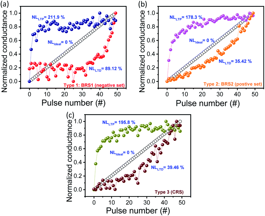 | ||
| Fig. 7 Normalized conductance of (a) type 1, (b) type 2, and (c) type 3 to extract the NL. | ||
For the high-density integration of the storage memory device, the sneak current issue in the cross-point array structure can be mitigated by CRS.39 The sneak current flows when a partial voltage is applied to adjacent cells of the target cell shown in Fig. 8(a). If all adjacent cells have LRS, the sneak current path leakage problem could be severe. To demonstrate a better read margin in CRS, a half-bias scheme is employed in the cross-point array structure.40 The worst case read margin41 is calculated as a function of the word line (WL) or bit line (BL) number for the three types of switching displayed in Fig. 8(b). CRS (type 3) shows the highest read margin among them because the current is suppressed at a low voltage regime. However, a CRS curve operating at a lower current as well as an additional selector element will be connected to each memory cell to ensure a larger array size.40 Table 1 compares the ON/OFF ratio, the endurance cycle, the linearity, the weight update error rate of potentiation and depression, and the read margin for the three types of switching.
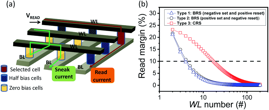 | ||
| Fig. 8 (a) Sneak current in cross-point structure, (b) read margin as a function of the number of WL for three types of switching. | ||
| Type 1 (BRS1) | Type 2 (BRS2) | Type 3 (CRS) | |
|---|---|---|---|
| ON/OFF ratio | >10 | <10 | <10 |
| Endurance cycles | 200 | 100 | 50 |
| Number of word lines at read margin (10%) | 4 | 3 | 17 |
| LTP/LTD NL (%) | 211.9/89.12 | 178.3/35.42 | 195.8/39.46 |
| LTP/LTD weight update error (%) | 44.9/40.8 | 38.78/24.48 | 40.8/44.89 |
The Pt/HfAlOx/TiN device shows good stability as well as multilevel and tunable switching based on different measurement conditions such as CC,42 bias polarity, and voltage sweep range,43 which are explained in the flow chart presented in the inset in Fig. 9. LRS current is well controlled by CC (see Fig. S3, ESI†). By increasing CC from 700 μA to 2 mA, the BRS1 (200 cycles) behavior turns to CRS (50 cycles), as shown in Fig. 9. We can then select type 1 or type 2 from CRS depending on the CC. The I–V curves (type 2, positive set and negative reset) are similar to the interface-type when a smaller voltage stop is used at positive bias. Interface-type switching is well known for its poor retention,44 and we confirmed the current decay by short-term memory effect in pulse train (see Fig. S4, ESI†). There is no specific CC because the switching occurs before the effective current change. Fifty endurance cycles are observed in this switching mode, as shown in Fig. 9. Further, when a higher CC of 4 mA is newly applied at type 3 (CRS) at CC of 2 mA, the switching mode returns to type 1 (BRS1). The tendency for the LRS current to gradually increase is observed for the conversion to be completed, and 450 DC cycles of endurance are conducted after the stabilization (see Fig. S5, ESI†). The CC dependent switching tendency suggests that low CC (700 μA) can limit the reset process after the set process for CRS and high CC (4 mA). The possible conduction filament evolution model for the transition from BRS to CRS can be explained by the schematics based of previous literature about metal oxide-based RRAM devices (see Fig. S6, ESI†).45–49
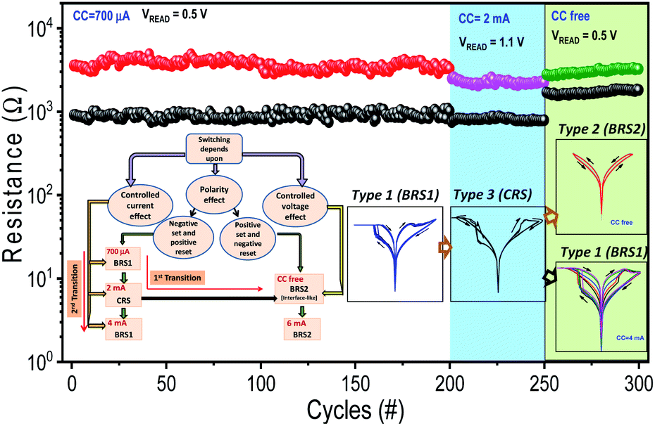 | ||
| Fig. 9 Continuous endurance cycle for three switching types (BRS1 → CRS → BRS2) and flow chart and I–V curves for the transition among different switching types. | ||
Conclusion
We characterize three types of resistive switching behaviors in a Pt/HfAlOx/TiN device for neuromorphic application. Type 1 (BRS1 under negative set and positive reset) shows the best endurance and ON/OFF margin. Type 2 (BRS2 under positive set and negative reset) shows the weight update with the best linear manner and the lowest variation by identical pulses. Type 3 (CRS, the reset after the set process in the same polarity) is advantageous in the sense that it has the highest read margin in a cross-point array structure due to the nonlinear I–V characteristics. Moreover, with the same polarity, the increase and the decrease of the conductance can be controlled by the magnitude of the pulse. Finally, the transitions between BRS and CRS are verified by controlling the operation polarity and the CC. Various resistive switching characteristics according to the operation switching mode in one device can be flexibly applied to various applications including neuromorphic system.Conflicts of interest
There are no conflicts to declare.Acknowledgements
This work is supported by the National Research Foundation of Korea (NRF), grant funded by the Korean government (MSIP) under Grant 2018R1C1B5046454 and supported by the Dongguk University Research Fund of 2020.Notes and references
- Y. Chen, G.-Y. Jung, D. A. A. Ohlberg, X. Li, D. R. Stewart, J. O. Jeppesen, K. A. Nielsen, J. F. Stoddart and R. S. Williams, Nanotechnology, 2003, 14, 462–468 CrossRef CAS.
- M. D. Pickett and R. William, Nanotechnology, 2012, 23, 215202 CrossRef PubMed.
- B. Gao, X. Shimeng, N. Liu, B. Liu and B. Wang, IEEE Int. Electron Devices Meet., 2008, 1–4 Search PubMed.
- F. Pan, S. Gao, C. Chen, C. Song and F. Zeng, Mater. Sci. Eng., R, 2014, 83, 1–59 CrossRef.
- D. Ielmini and H. S. P. Wong, Nat. Electron., 2018, 1, 333–343 CrossRef.
- W. Bai, R. Huang, Y. Cai, Y. Tang, X. Zhang and Y. Wang, IEEE Electron Device Lett., 2013, 34, 223–225 CAS.
- Y. Wang, Q. Liu, S. Long, W. Wang and Q. Wang, et al., Nanotechnology, 2009, 21, 045202 CrossRef PubMed.
- S. H. Jo, T. Chang, I. Ebong, B. B. Bhadviya, P. Mazumder and W. Lu, Nano Lett., 2010, 10, 1297–1301 CrossRef CAS PubMed.
- T. Sekitani, T. Yokota, U. Zschieschang, H. Klauk, S. Bauer, K. Takeuchi and M. Takamiya, et al., Science, 2009, 326, 1516–1519 CrossRef CAS PubMed.
- S. Yu, Y. Wu, R. Jeyasingh and D. Kuzum, et al., IEEE Trans. Electron Devices, 2011, 58, 2729–2737 CAS.
- Q. Wan, M. T. Sharbati, J. R. Erickson, Y. Du and F. Xiong, Adv. Mater. Technol., 2019, 4, 1900037 CrossRef.
- V. Milo, C. Zambelli, P. Olivo, E. Pérez, M. K. Mahadevaiah, O. G. Ossorio, Ch. Wenger and D. Ielmini, APL Mater., 2019, 7, 081120 CrossRef.
- F. Pan, S. Gao, C. Chen, C. Song and F. Zeng, Mater. Sci. Eng., R, 2014, 83, 1–59 CrossRef.
- C. D. Wright, P. Hosseini and J. A. V. Diosdado, Adv. Funct. Mater., 2013, 23, 2248–2254 CrossRef CAS.
- A. Wedig, M. Luebben, D. Cho, M. Moors, K. Skaja and I. Valov, Nat. Nanotechnol., 2016, 11, 67–74 CrossRef CAS PubMed.
- Y. X. Zhou, Y. Li, Y. T. Su, Z. R. Wang, L. Y. Shih, T. C. Chang, K. C. Chang, S. B. Long, S. M. Sze and X. S. Miao, Nanoscale, 2017, 9, 6649–6657 RSC.
- R. Degraeve, A. Fantini, N. Raghavan, L. Goux, S. Clima, B. Govoreanu, A. Belmonte, D. Linten and M. Jurczak, Microelectron. Eng., 2015, 147, 171–175 CrossRef CAS.
- S. Yu, B. Gao, H. Dai, B. Sun, L. Liu, X. Liu, R. Han, J. Kang and B. Yu, Electrochem. Solid-State Lett., 2010, 13, 36 CrossRef.
- X. Di Huang, Y. Li, H. Y. Li, Y. F. Lu, K. H. Xue and X. S. Miao, Appl. Phys. Lett., 2020, 116, 173504 CrossRef.
- M. Akbari, M. K. Kim, D. Kim and J. S. Lee, RSC Adv., 2017, 7, 16704–16708 RSC.
- B. Gao, B. Chen, F. Zhang, L. Liu and Yu. Bin, IEEE Trans. Electron Devices, 2013, 60, 1379–1383 CAS.
- S. La Barbera, A. F. Vincent, D. Vuillaume, D. Querlioz and F. Alibart, Sci. Rep., 2016, 6, 1–11 CrossRef PubMed.
- G. Wang, S. Long, Z. Yu, M. Zhang, Y. Li, D. Xu, H. Lv, Q. Liu, X. Yan, M. Wang, X. Xu, H. Liu, B. Yang and M. Liu, Nanoscale Res. Lett., 2015, 10, 1–7 CrossRef CAS PubMed.
- C.-Y. Lin, C.-Y. Wu, C.-Y. Wu, C. Hu and T.-Y. Tseng, J. Electrochem. Soc., 2007, 154, G189 CrossRef CAS.
- U. Celano, Y. Yin Chen, D. J. Wouters, G. Groeseneken, M. Jurczak and W. Vandervorst, Appl. Phys. Lett., 2013, 102, 121602 CrossRef.
- J. K. Lee, S. Jung, J. Park, S. W. Chung, J. Sung Roh, S. J. Hong, I. Hwan Cho, H. I. Kwon, C. Hyeong Park, B. G. Park and J. H. Lee, Appl. Phys. Lett., 2012, 101, 103506 CrossRef.
- S. G. Hu, Y. Liu, T. P. Chen, Z. Liu, Q. Yu, L. J. Deng, Y. Yin and S. Hosaka, Appl. Phys. Lett., 2013, 102, 183510 CrossRef.
- B. Granseth, B. Odermatt, S. J. J. Royle and L. Lagnado, Neuron, 2006, 51, 773–786 CrossRef CAS PubMed.
- R. Yang, H. Huang and X. Guo, Adv. Electron. Mater., 2019, 5, 1900287 CrossRef.
- G. G. Turrigiano and S. B. Nelson, Nat. Rev. Neurosci., 2004, 5, 97–107 CrossRef CAS PubMed.
- P. P. Atluri and W. G. Regehr, J. Neurosci., 1996, 16, 5661–5671 CrossRef CAS PubMed.
- S. A. Baccus, Proc. Natl. Acad. Sci. U. S. A., 1998, 95, 8345–8350 CrossRef CAS PubMed.
- R. Guo, Y. Zhou, L. Wu, Z. Wang, Z. Lim, X. Yan, W. Lin, H. Wang, H. Y. Yoong, S. Chen, Ariando, T. Venkatesan, J. Wang, G. M. Chow, A. Gruverman, X. Miao, Y. Zhu and J. Chen, ACS Appl. Mater. Interfaces, 2018, 10, 12862–12869 CrossRef CAS PubMed.
- Y. T. Tseng, T. M. Tsai, T. C. Chang, C. C. Shih, K. C. Chang, R. Zhang, K. H. Chen, J. H. Chen, Y. C. Li, C. Y. Lin, Y. C. Hung, Y. E. Syu, J. C. Zheng and S. M. Sze, Appl. Phys. Lett., 2015, 106, 213505 CrossRef.
- T. Breuer, A. Siemon, E. Linn, S. Menzel and R. Vikas, Nanotechnology, 2015, 26, 415202 CrossRef PubMed.
- S. Yu, Proc. IEEE, 2018, 106, 260–285 CAS.
- G. Indiveri, E. Chicca and R. Douglas, IEEE Trans. Neural Network., 2006, 17, 211–221 CrossRef PubMed.
- G.-Q. Bi and M.-M. Poo, J. Neurosci., 1998, 24, 10464–10472 CrossRef.
- G. Khurana, N. Kumar, M. Chhowalla, J. F. Scott and R. S. Katiyar, Sci. Rep., 2019, 9, 1–10 CrossRef CAS PubMed.
- J. J. Huang, Y. M. Tseng, C. W. Hsu and T. H. Hou, IEEE Electron Device Lett., 2011, 32, 1427–1429 CAS.
- J. Zhou, K. H. Kim and W. Lu, IEEE Trans. Electron Devices, 2014, 61, 1369–1376 Search PubMed.
- J. T. Qiu, S. Samanta, M. Dutta, S. Ginnaram and S. Maikap, Langmuir, 2019, 35, 3897–3906 CrossRef CAS PubMed.
- Y. Lu, J. H. Lee and I. W. Chen, Nanoscale, 2017, 9, 12690–12697 RSC.
- F. Pan, C. Chen, Z. S. Wang, Y. C. Yang, J. Yang and F. Zeng, Prog. Nat. Sci.: Mater. Int., 2010, 20, 1–15 CrossRef.
- S. Chandrasekraran, F. M. Simanjuntak, R. Saminathan, D. Panda and T.-Y. Tseng, Nanotechnology, 2019, 30, 445205 CrossRef PubMed.
- D. Panda, A. Dhar and T.-Y. Tseng, IEEE Trans. Nanotechnol., 2012, 11, 51–55 Search PubMed.
- D. Panda and T.-Y. Tseng, Thin Solid Films, 2013, 531, 1–20 CrossRef CAS.
- D. Panda and T.-Y. Tseng, J. Mater. Sci., 2013, 48, 6849–6877 CrossRef CAS.
- D. Panda, C.-Y. Huang and T.-Y. Tseng, Appl. Phys. Lett., 2012, 100, 112901 CrossRef.
Footnote |
| † Electronic supplementary information (ESI) available. See DOI: 10.1039/d0ra06389d |
| This journal is © The Royal Society of Chemistry 2020 |